Article

A Fast Transient Response Capacitor-Less LDO with Transient Enhancement Technology

1
State Key Laboratory of ASIC and System, School of Microelectronics, Fudan University, Shanghai 200433, China
2
School of Electronic and Information Engineering, Soochow University, Suzhou 215006, China
*
Author to whom correspondence should be addressed.
Micromachines 2024, 15(3), 299; https://doi.org/10.3390/mi15030299
Submission received: 26 December 2023 / Revised: 17 February 2024 / Accepted: 19 February 2024 / Published: 22 February 2024
(This article belongs to the Special Issue Advanced Micro- and Nano-Manufacturing Technologies)

Abstract

:
This paper proposes a fast transient load response capacitor-less low-dropout regulator (CL-LDO) for digital analog hybrid circuits in the 180 nm process, capable of converting input voltages from 1.2 V to 1.8 V into an output voltage of 1 V. The design incorporates a rail-to-rail input and push–pull output (RIPO) amplifier to enhance the gain while satisfying the requirement for low power consumption. A super source follower buffer (SSFB) with internal stability is introduced to ensure loop stability. The proposed structure ensures the steady-state performance of the LDO without an on-chip capacitor. The auxiliary circuit, or transient enhancement circuit, does not compromise the steady-state stability and effectively enhances the transient performance during sudden load current steps. The proposed LDO consumes a quiescent current of 47 µA and achieves 25 µV/mA load regulation with a load current ranging from 0 to 20 mA. The simulation results demonstrate that a settling time of 0.2 µs is achieved for load steps ranging from 0 mA to 20 mA, while a settling time of 0.5 µs is attained for load steps ranging from 20 mA to 0 mA, with an edge time of 0.1 µs.

1. Introduction

Power management ICs (PMICs) are essential components in electronic devices that require efficient power management [1]. Low-dropout regulators (LDOs) are preferred over other voltage regulators due to their low noise, low ripple, low quiescent current and high power supply rejection ratio (PSRR) [2,3,4,5]. To satisfy the different voltage regulation requirements of various modules in a single system-on-chip (SOC), multiple voltage regulators can be integrated on the same chip. This approach can reduce the power dissipation and improve the overall efficiency of the system. In SoC designs, LDOs are commonly used to supply power to analog or mixed-signal modules, which are particularly sensitive to noise and voltage fluctuations [6,7,8]. However, the traditional LDO architecture relies on a large capacitor, which occupies a large area and reduces circuit integration. Removal of this large off-chip capacitor will inevitably degrade the performance requirements of the LDO, especially stability, transient response and PSRR. Therefore, in recent years, capacitor-less LDOs (CL-LDOs) have been widely studied and reported [9,10,11].
A series of techniques have been proposed to improve the transient response of CL-LDO [12,13,14,15,16,17]. Using a flipped voltage follower (FVF) to separate the dominant poles in conventional LDO is one of the most popular methods. The FVF and overshoot detection circuit used in [12] reduce the overshoot/undershoot voltages of LDO and achieve fast settling times during load steps. The push–pull amplifier is a kind of architecture that can be used to provide a fast response to load and line transients [13,15]. The LDO with Class-AB OTA in [13] provides not only a fast response to load and line transients, but also handles a wide range of load capacitors, while the push–pull output stage-based LDO in [15] can achieve a 2.7 µs settling time with the load current switching from 100 pA to 100 mA. A dynamic biasing technique is widely used, whereby the bias current of the LDO is adjusted based on the load current. This can improve the efficiency of the LDO and reduce the power dissipation. To enhance both the transient and stability, Li et al. proposed a CL-LDO based on dual-active feedback frequency compensation that ultimately guarantees stable operation in a load range of 0 to 100 mA [14]. In [17], the authors use modified Miller compensation with the insertion of a sensor amplifier stage to inject more transient current in the biasing circuit. This method feeds the regulator to rapidly charge the power PMOS gate capacitance and improves the fast transient response.
This work proposes a novel CL-LDO circuit with a fast transient response. Section 2 demonstrates the complete architecture with a rail-to-rail input, push–pull output (RIPO) two-stage amplifier and a super source follower buffer (SSFB) and analyzes the stability and transient response. Section 3 presents a design example, validated through simulation results, and compares this work with others. Section 4 summarizes the conclusion.

2. Proposed CL-LDO Architecture with RIPO and SSFB

2.1. Conventional Topology of LDO

The traditional LDO topology with an off-chip capacitor depicted in Figure 1 exhibits three poles and a left-half-plane zero without the need for an auxiliary circuit. The stability of this system is ensured by the presence of a left-half-plane zero, which is generated by the output capacitor with a capacitance in the microfarad range and its equivalent resistance. Additionally, Equation (1) establishes that the dominant pole is positioned at the output node. The remaining two poles are positioned at the output of the amplifier and feedback resistance. The removal of this bully output capacitor poses a greater challenge to the stability. To enhance the stability, compensation capacitors are added in the auxiliary circuit.
P 1 = 1 R 1 + R 2 R L r o p C L + C O
The spike output voltage in the LDO when there are sudden changes in the load current from other cells is also depicted in Figure 1. The unity gain frequency (UGF) is one of the most essential factors of transient performance. To achieve a large UGF, prior studies have proposed an architecture incorporating a buffer as the auxiliary circuit to decouple the high impedance from the EA’s output and the large capacitance from the MP’s input. Additionally, the response time TR [12] of the LDO can be approximated as Equation (2):
T R 1 BW + C par Δ V G I G
where BW denotes the loop bandwidth, Cpar represents the parasitic cap, ΔVG refers to the required voltage change and IG represents the slewing current at MP’s gate. The buffer with a low output resistance can offer a high slewing current to rapidly respond to the load step.

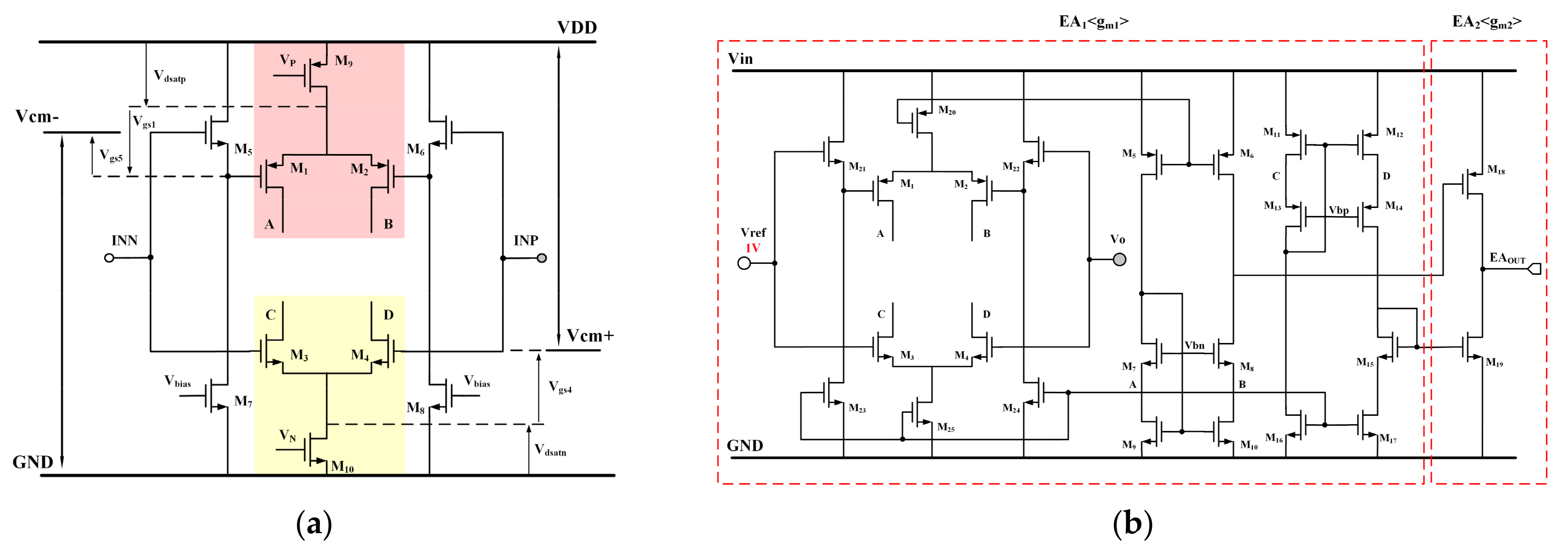
2.2. Proposed RIPO and SSFB

A rail-to-rail input of the RIPO amplifier is shown in Figure 2a. The PMOS input pair M1–M2 is utilized to achieve the negative supply rail, while the NMOS input pair M3–M4 is employed to reach the positive supply rail. The transistors M5 to M8 are used as level shifters for the PMOS input pair, thereby expanding the negative input range to ensure that the PMOS input pair operates in the saturation region. The tail currents of two complementary input pairs are supported by M9 and M10. The positive supply rail extends from Vcm+ to VDD, while the negative supply rail spans from GND to Vcm−. The expressions for Vcm+ and Vcm− are represented by Equation (3) and Equation (4), respectively:
V c m + = V d s a t n + V g s 4
V c m = V D D V d s a t p V g s 1 + V g s 5 V D D V d s a t p
where Vdsatn and Vdsatp are the minimum drain–source voltages that ensure M9 and M10 operate as current sources. When VDD > Vgs4 + Vdsatn + Vdsatp = Vgs + 2Vdsat, the input range is obviously from 0 to VDD. The complete RIPO amplifier circuit is depicted in Figure 2b. It is based on the compact cascode amplifier (EA1) with rail-to-rail input, where the gate voltage of EA2 is sourced from the output of EA1. When the voltage of INP, the negative input of EA1, increases, the voltages of b and d decrease simultaneously. In this case, both gate voltages of M24 and M25 are reversed from INP and in phase at INN. So, the output stage, EA2, functions as a push–pull amplifier in the RIPO circuit. The stability analysis of this RIPO amplifier configuration with CC1 is addressed in Section 2.3.
The proposed SSFB added as an auxiliary circuit is shown in Figure 3. The core components of the SSFB are M26–M28, where the M26 is used as the source follower, while M27 and M28 serve to enhance the following capability. The primary signal transmission pathway involves the passage of signals from the gate of M26 through resistor Rz to reach the output terminal. The node at the gate of M27 is a high impedance node. Generally, the stability of a buffer solely based on this main signal path is not taken into consideration. However, it should be noted that the proposed buffer also incorporates an inner loop, which may cause stability problems. To deal with the stability issue, compensation is achieved by incorporating capacitor CB and resistors RB RZ. A detailed analysis is provided in Section 2.3. The transistors M31 and M36 are used as current sources to supply the static operating currents Ibp and Ibn, respectively. The ratio of Ibp to Ibn is set at 1:4, with Ibp biased at 0.25 µA and Ibn biased at 1 µA.

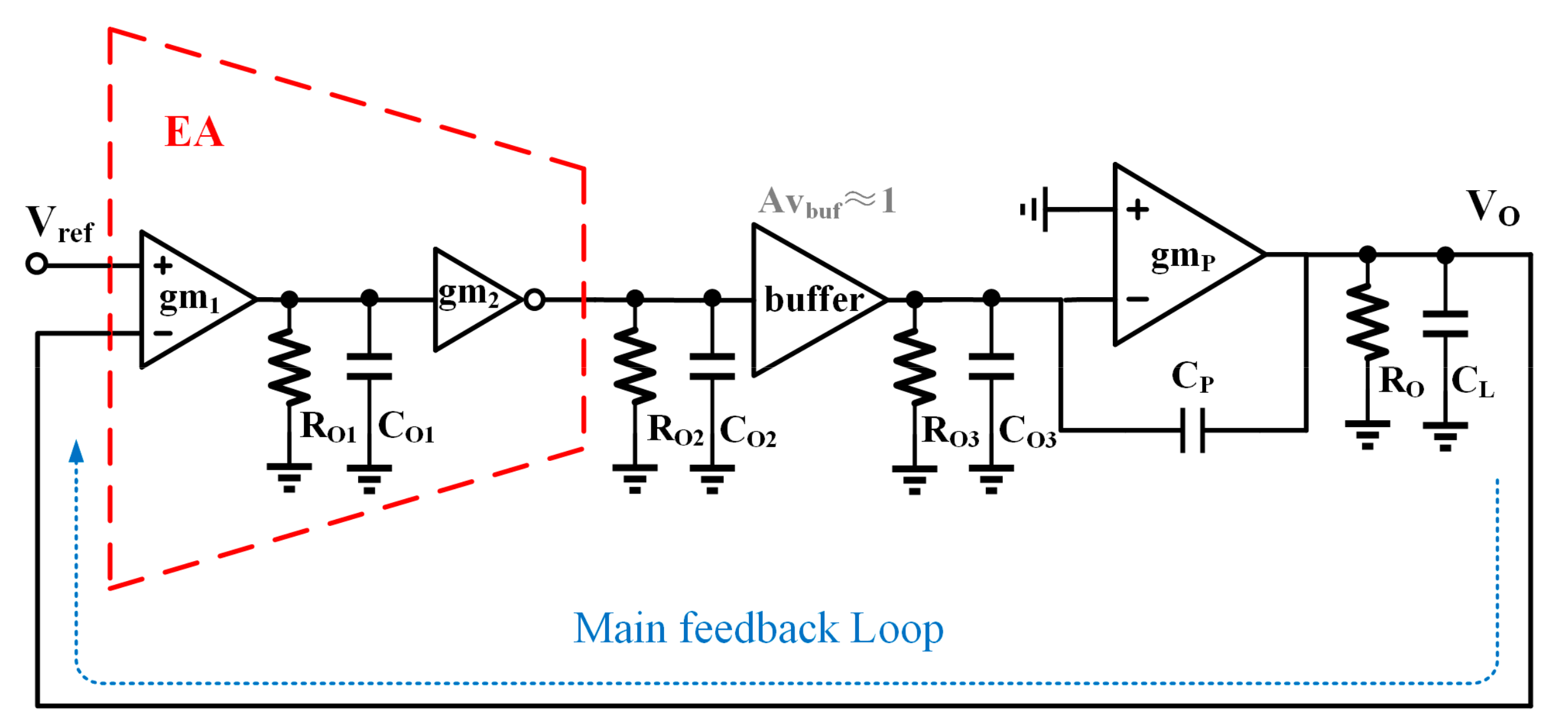
2.3. Stability Analysis

The simplified structure of the whole CL-LDO with RIPO and SSFB is illustrated in Figure 4. The main feedback loop of the LDO consistently employs linear feedback, and this paper uses the unit negative feedback. Considering that the transfer function of the buffer is close to unity except at high frequencies, and considering its large input impedance, we temporarily substitute it with Avbuf ≈ 1 when analyzing the frequency response of CL-LDO. This is discussed separately later. The pole inside EA, which is at an extremely high frequency due to the small parasitic capacitance CO1 and is composed of the output of EA1 and input of EA2, is disregarded in the frequency response analysis of the proposed CL-LDO. RO2 and CO2 stand for the output resistance of EA and the input parasitic capacitor of the buffer, respectively. CO3 comprises the gate–source capacitor (Cgs) of the power PMOS MP and the output parasitic capacitor of the buffer. Considering that the parasitic capacitance is significantly smaller than Cgs by several orders of magnitude, it can be approximated that CO3 is approximately equal to Cgs. RO3 is equal to the output resistance of the super source buffer, which is extremely small. CgP consists of the Miller compensation capacitor, CP, and the gate–drain capacitor (CgP) of MP. The resistance RO denotes the equivalent output resistance, which is influenced by the load current, while CL represents the load capacitor. The Av(s) is given by Equations (5)–(9).
A v s = V o u t s V i n s A d c 1 s C g P g m P 1 + s p 1 1 + s p 2 1 + s p 3
A d c = g m 1 R O 1 × g m 2 R O 2 × A v b u f × g m P R O
P 1 1 R O 3 C O 3 + 1 + g m P R O C g P
P 2 1 + g m P R O C P + C O 3 R O C L C P + C P C O 3 + C L C O 3
P 3 = 1 R O 2 C O 2
P1 is the dominant pole, while P2 and P3 are the non-dominant poles. When the load current Iload increases, the output resistance decreases due to its inverse proportionality with the load current. Since gmp is proportional to I l o a d and RO is proportional to 1/Iload, P1 and P2 are proportional to I l o a d . To guarantee system stability, the phase margin should be above 60°; so, P2 and P3 should be placed above the double unity gain frequency under all conditions. The approximate output resistance of EA RO2 = r O 24 | | r O 25 is several megaohms, while the equivalent capacitor at the input of MP is approximately tens of pF. Without the proposed buffer, the non-dominant pole is generated by the resistance RO2 and capacitors Cgs and Cgd, which are near to the dominant pole, thereby leading to stability issues. However, in this paper, the buffer incorporating a low output resistance separates this low-frequency pole into two high-frequency poles. The frequency response when Iload changes is shown in Figure 5. The circuit could keep steady when Iload rises to 20 mA without an output capacitor.
The stability of the entire proposed loop must be ensured under all conditions, along with the buffer stability, which has been approximately replaced by Avbuf,. To analyze the loop stability of the buffer, the block diagram in Figure 6 is proposed. The resistor RZ is added to generate a zero with the parasitic capacitor Cgp. The presence of this zero ensures the stable operation of the inner loop, even when Cgp is large and, in turn, generates another pole for the main feedback loop. The capacitor CB and resistor RB are also added to compensate. Although the Miller gain applied to CB is relatively small, it should be noted that one end of CB is connected to the drain of M24. Consequently, to facilitate a simplified analysis within the block diagram, both CB and RB are connected in series and grounded. The gain of the inner loop is approximately given by Equation (10).
A v l o o p g m 27 r o 31 1 + s R B C B 1 + s R Z C g p 1 + s r o 31 C B 1 + s R Z C g p

2.4. Transient Response Analysis

The proposed CL-LDO is expected to exhibit an enhanced transient response and reduced undershoot and overshoot spikes. To enhance the transient response, the dynamic charging transistors are added to deal with large transient steps. As depicted in Figure 7, the gate of PMOS MDCp and NMOS MDCn is directly regulated by the voltages Vd of the d node and Vb of the b node in the folded cascode amplifier. The ratio of the size of MDCTp to MDCTn is set as 1:2. At steady state, the MDCn and MDCp transistors are biased in the cutoff region by Vb and Vd because the overdrive voltages of both M16 and M18 are lower than the threshold voltages of MDCn and MDCp. In this case, this transient enhancement circuit will not influence the stability even with some offset at the input pairs. However, when a large transient step occurs, the output voltage will increase or decrease instantly. Since Vb and Vd are naturally sensitive to the transient response, large current Icharge and Idischarge can be generated to charge or discharge the large gate parasitic capacitor of MP without additional sensing circuits. The deviation of the output voltage Vdev that causes Vb and Vd to bias dynamic charging transistors in open mode is given in Equations (11) and (12).
V d e v p = V t h , M D C T p V o v 12 g m n R d
V d e v n = V t h , M D C T n V o v 10 g m p R b
where Vth,MDCTp and Vth,MDCTn are the threshold of MDCp and MDCn, and where Vov12 and Vov10 are the overdrive voltages of M12 and M10. Here, gmp and gmn stand for the trans-conductance of the input pair consisting of M1,2 and M3,4, while Rd and Rb denote the equivalent resistance at nodes d and b, respectively. When considering the size of MDCp and MDCn, due to the presence of a small parasitic capacitance, the minimum length is used to ensure a rapid response time. According to the equation, it is evident that Vdevp,n is controlled by the threshold voltage of MDCp,n. However, if the transistor’s size and voltages of the b and d nodes are appropriately designed, Vdevp,n will be constrained by the gain of this transient enhancement circuit and will remain unaffected by Vth,MDCp,n. Additionally, a smaller Vdevp,n leads to a reduced ΔVOUT. To effectively regulate the overshoot and undershoot voltage at one-tenth of VOUT, it is recommended that Vdevp,n be set to approximately 100 mV.
To control the transient response limitation caused by the finite bandwidth of the main linear regulation loop, a simple operational trans-conductance amplifier (OTA) with a constant small current is incorporated to regulate the high impedance node of the proposed SSFB. By employing this simple OTA for control, the unity gain frequency can be pushed to a higher point and the bandwidth of the main loop can be expanded. The loop frequency response of the whole circuit with added OTA is shown in Section 3 to demonstrate the stability.

3. Simulation Results and Discussion

The proposed CL-LDO is simulated using a TSMC 0.18 μm standard CMOS process. With a supply voltage range of 1.2 V to 1.8 V and a bias current of 2 µA, this CL-LDO is designed to maintain output voltage regulation at 1 V. We will talk about the precise simulation findings for the stability, load regulation, line regulation, and power supply rejection under various conditions.

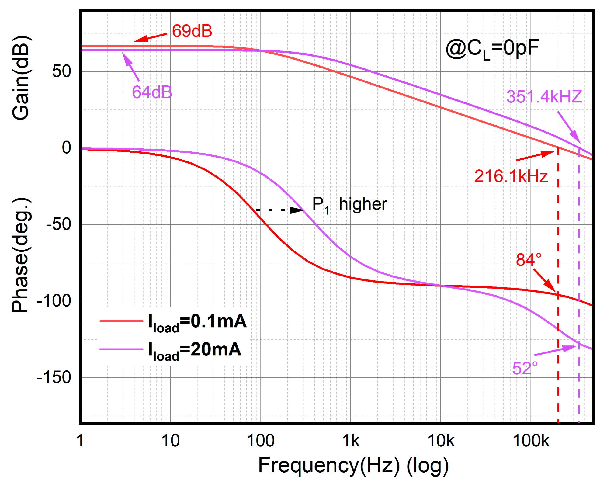
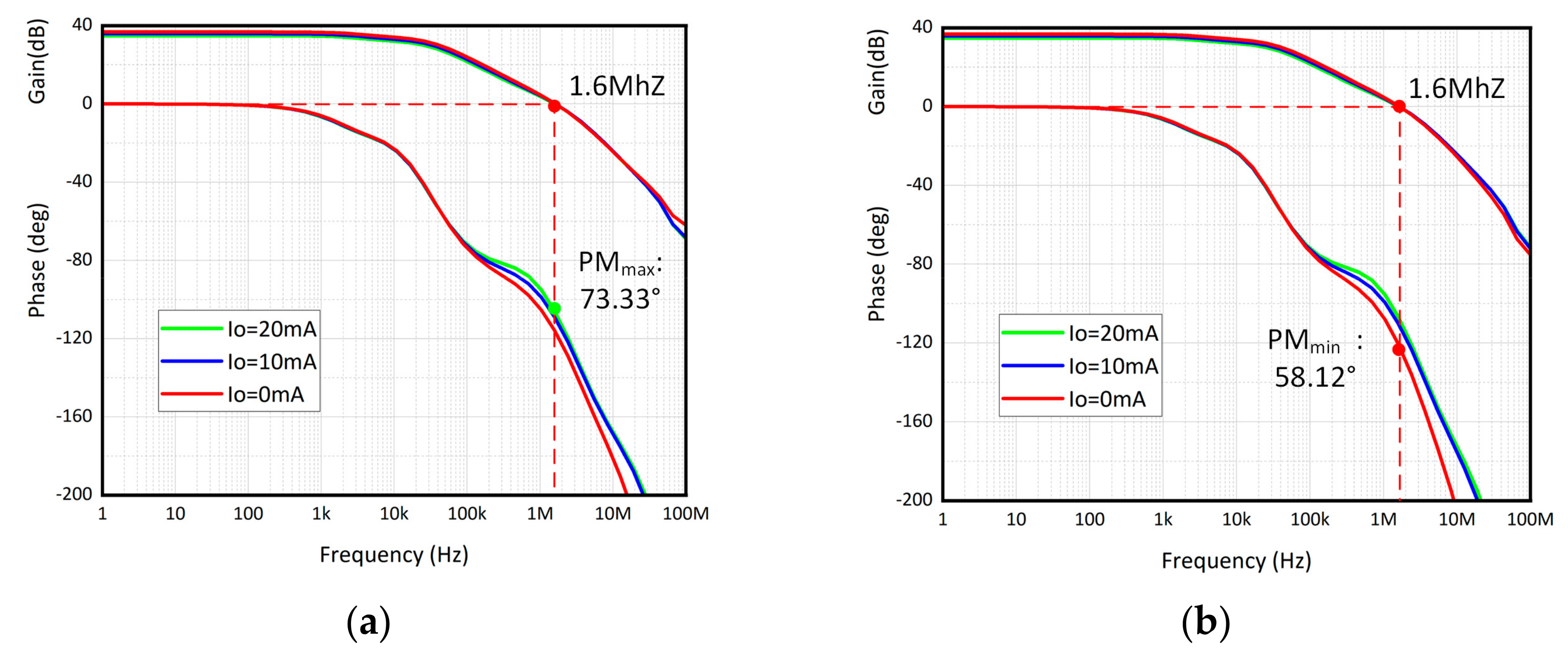
3.1. Loop Frequency Response

The loop frequency response under different load capacitor and load current combinations is shown in Figure 8. Figure 8a shows the Bode diagram without load capacitor, while Figure 8b shows the load capacitor at 100 pF. Both (a) and (b) show the current load range from 20 mA to 0 mA. As previously analyzed, the bandwidth is pushed from several hundred kilohertz to 1.6 megahertz. On the contrary, the dc gain decreases by approximately 30 dB, which demonstrates the trade-off between gain and speed. It is evident that the load condition has little influence on stability since the node at output is set as the non-dominant pole. The minimum phase margin is 58.12° when the load current is 0 mA and the load capacitor is 100 pF. Meanwhile, the maximum phase margin is 73.33° when the load current is 20 mA and without a load capacitor.

3.2. Load Transient Response and Load Regulation

The load transient response and load regulation of the proposed CL-LDO are depicted in Figure 9. The load current ranges from 0 A to 20 mA, while the rise and fall times of ILoad for emulating the load transient response are set at 100 ns. The simulation results of CL-LDO with and without the transient enhancement circuit are compared and illustrated in Figure 9a. The response time of CL-LDO during load current rise and fall is significantly improved, with a reduction to 0.2 µs and 0.5 µs, respectively, surpassing the performance of the circuit without a transient enhancement circuit. The undershoot voltage drops from 566.5 mV to 238.6 mV, and the overshoot voltage drops from 437.6 mV to 156 mV. Figure 9b shows the load regulation when VIN = 1.8 V and CL = 0 pF. The VOUT suffers from a 530 µV variation when ILoad changes from 0 to 20 mA, resulting in a load regulation of 26.5 µV/mA.

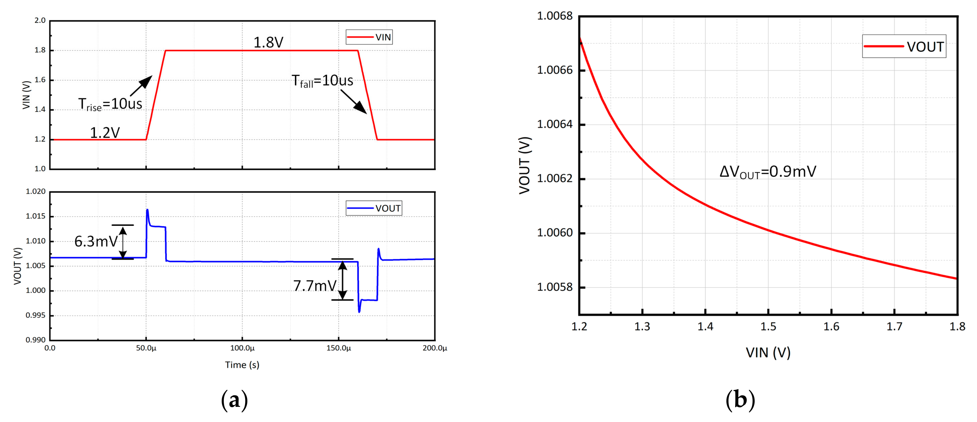
3.3. Line Transient Response and Line Regulation

Figure 10a illustrates the line transient response when the VIN step is between 1.2 V and 1.8 V at an edge time of 10 µs of the proposed CL-LDO. The line transient response is simulated at CL = 100 pF and IO = 0 mA. The output voltage exhibits an overshoot of 6.3 mV when the VIN steps up. Conversely, it experiences an undershoot of 7.7 mV when the line regulation, which quantifies the deviation in output voltage, is simulated under identical conditions. The voltage output, as depicted in Figure 10b, exhibits a variation of 0.9 mV, resulting in a line regulation of 1.5 mV/V.

3.4. Power-Supply Rejection

The PSR of an LDO is given in [18], as shown in Equation (13).
P S R = v o u t s v i n s = R L R L + r d s 1 + s ω 0 1 + L G s
where LG(s) stands for the loop gain, ω0 is the pole at the output of the LDO, and RL and rds denote the load resistance and the output impedance of MP, respectively. At low frequency, PSR is obviously equal to 1/(1 + LG(s)). If the ω0 is the non-dominant pole, the loop gain exhibits a roll-off at −20 dB/decade, resulting in a corresponding decline in the PSR at the same rate from the dominant pole. This degradation will persist until the PSR remains constant when LG(s) is significantly smaller than 1. At a higher frequency, the PSR is primarily influenced by the load capacitor and the MP’s parasitic capacitors, resulting in a reduction in the equivalent resistance. The simulated PSR performance of the proposed CL-LDO at a 20 mA load current and 0 pF load capacitor is shown in Figure 11. The PSR of the proposed CL-LDO is −43 dB at 100 Hz and −9 dB at 1 MHz. The attenuation trend of PSR degrades by −20 dB/decade after the dominant pole, which corresponds to the analysis of Equation (13) and the stability analysis.

3.5. Performance Comparison

The figure of merit (FOM) in [19,20] is adopted to evaluate the different current efficiencies of the CL-LDOs. The smaller FOM indicates superior performance in terms of the current efficiency and load transient response. The parasitic capacitance of the power transistor is influenced by the minimum channel length (L) in different processes. A process with a shorter minimum L may result in a smaller FOM due to the reduced parasitic capacitance of the transistor. To ensure a fair comparison, the FOM1 equation, originally proposed in [6] with consideration of the minimum L, is used to compare the transient response.
F O M 1 = T e d g e Δ V O U T I Q + I L o a d ( min ) Δ I L o a d L 2
The performance comparison with previously reported CL-LDOs is summarized in Table 1. In this table, the representative study findings from recent years are compared with this design to demonstrate the improved performance. The IQ row shows that the power consumption of this design is only slightly higher than that proposed in 2020, and significantly lower than other architectures. The Load Reg and Tsettle rows show that this design can achieve good voltage regulation and a fast response performance when the load current changes. These comparison results demonstrate that even under the relatively backward 180 nm process, the architecture can still have lower power consumption, smaller load regulation and a faster response speed. As a result, this demonstrates a lower FOM1, indicating a higher performance benefit.

4. Conclusions

This paper proposes a new capacitor-less LDO structure for digital analog hybrid circuits. The proposed capacitor-less LDO utilizes RIPO and SSFB to satisfy the design challenge of stability typically associated with the absence of on-chip capacitors. This proposed structure is stable at a load current range of 0 mA to 20 mA, with a maximum allowable CL of 100 pF. With the transient enhancement circuit, this structure achieves a good transient response while ensuring stability. The settling time is about 0.22 µs when the load current steps from 0 mA to 20 mA within 100 ns.

Author Contributions

Conceptualization, C.C. and M.S.; Methodology, C.C., M.S., L.W. and T.H.; Software, C.C. and T.H.; Validation, C.C.; Formal analysis, C.C., M.S., L.W. and T.H.; Investigation, C.C.; Resources, M.X.; Data curation, C.C.; Writing—original draft, C.C.; Writing—review & editing, C.C., M.S., T.H. and M.X.; Supervision, M.X.; Project administration, M.X. All authors have read and agreed to the published version of the manuscript.

Funding

This research received no external funding.

Data Availability Statement

Data are contained within the article.

Conflicts of Interest

The authors declare no conflict of interest.

References

  1. Ho, E.N.Y.; Mok, P.K.T. A Capacitor-Less CMOS Active Feedback Low-Dropout Regulator with Slew-Rate Enhancement for Portable On-Chip Application. IEEE Trans. Circuits Syst. II Express Briefs 2010, 57, 80–84. [Google Scholar] [CrossRef]
  2. Lu, Y.; Wang, Y.; Pan, Q.; Ki, W.-H.; Yue, C.P. A Fully-Integrated Low-Dropout Regulator with Full-Spectrum Power Supply Rejection. IEEE Trans. Circuits Syst. I Regul. Pap. 2015, 62, 707–716. [Google Scholar] [CrossRef]
  3. Patel, A.P.; Rincon-Mora, G.A. High Power-Supply-Rejection (PSR) Current-Mode Low-Dropout (LDO) Regulator. IEEE Trans. Circuits Syst. II Express Briefs 2010, 57, 868–873. [Google Scholar] [CrossRef]
  4. Lavalle-Aviles, F.; Torres, J.; Sanchez-Sinencio, E. A High Power Supply Rejection and Fast Settling Time Capacitor-Less LDO. IEEE Trans. Power Electron. 2019, 34, 474–484. [Google Scholar] [CrossRef]
  5. Yadav, B.B.; Mounika, K.; De, K.; Abbas, Z. Low Quiescent Current, Capacitor-Less LDO with Adaptively Biased Power Transistors and Load Aware Feedback Resistance. In Proceedings of the 2020 IEEE International Symposium on Circuits and Systems (ISCAS), Seville, Spain, 12–14 October 2020; pp. 1–5. [Google Scholar]
  6. Hong, S.W.; Cho, G.H. High-Gain Wide-Bandwidth Capacitor-Less Low-Dropout Regulator (LDO) for Mobile Applications Utilizing Frequency Response of Multiple Feedback Loops. IEEE Trans. Circuits Syst. I Regul. Pap. 2016, 63, 46–57. [Google Scholar] [CrossRef]
  7. Kim, S.J.; Chang, S.B.; Seok, M. A High PSRR, Low Ripple, Temperature-Compensated, 10-μA-Class Digital LDO Based on Current-Source Power-FETs for a Sub-mW SoC. IEEE Solid-State Circuits Lett. 2021, 4, 88–91. [Google Scholar] [CrossRef]
  8. Lu, Y.; Ki, W.-H.; Yue, C.P. 17.11 A 0.65ns-response-time 3.01ps FOM fully-integrated low-dropout regulator with full-spectrum power-supply-rejection for wideband communication systems. In Proceedings of the 2014 IEEE International Solid- State Circuits Conference (ISSCC), San Francisco, CA, USA, 9–13 February 2014; pp. 306–307. [Google Scholar]
  9. Torres, J.; El-Nozahi, M.; Amer, A.; Gopalraju, S.; Abdullah, R.; Entesari, K.; Sanchez-Sinencio, E. Low Drop-Out Voltage Regulators: Capacitor-less Architecture Comparison. IEEE Circuits Syst. Mag. 2014, 14, 6–26. [Google Scholar] [CrossRef]
  10. Khan, M.; Chowdhury, M.H. Capacitor-less Low-Dropout Regulator (LDO) with Improved PSRR and Enhanced Slew-Rate. In Proceedings of the 2018 IEEE International Symposium on Circuits and Systems (ISCAS), Florence, Italy, 27–30 May 2018; pp. 1–5. [Google Scholar]
  11. Leo, C.J.; Raja, M.K.; Minkyu, J. An ultra low-power capacitor-less LDO with high PSR. In Proceedings of the 2013 IEEE MTT-S International Microwave Workshop Series on RF and Wireless Technologies for Biomedical and Healthcare Applications (IMWS-BIO), Singapore, 9–11 December 2013; pp. 1–3. [Google Scholar]
  12. Liu, N.; Chen, D. A Transient-Enhanced Output-Capacitorless LDO with Fast Local Loop and Overshoot Detection. IEEE Trans. Circuits Syst. I Regul. Pap. 2020, 67, 3422–3432. [Google Scholar] [CrossRef]
  13. Raducan, C.; Grajdeanu, A.-T.; Plesa, C.-S.; Neag, M.; Negoita, A.; Topa, M.D. LDO With Improved Common Gate Class-AB OTA Handles any Load Capacitors and Provides Fast Response to Load Transients. IEEE Trans. Circuits Syst. I Regul. Pap. 2020, 67, 3740–3752. [Google Scholar] [CrossRef]
  14. Li, G.; Qian, H.; Guo, J.; Mo, B.; Lu, Y.; Chen, D. Dual Active-Feedback Frequency Compensation for Output-Capacitorless LDO with Transient and Stability Enhancement in 65-nm CMOS. IEEE Trans. Power Electron. 2020, 35, 415–429. [Google Scholar] [CrossRef]
  15. Qu, X.; Zhou, Z.-K.; Zhang, B.; Li, Z.-J. An Ultralow-Power Fast-Transient Capacitor-Free Low-Dropout Regulator with Assistant Push–Pull Output Stage. IEEE Trans. Circuits Syst. II Express Briefs 2013, 60, 96–100. [Google Scholar] [CrossRef]
  16. Ho, M.; Leung, K.N.; Mak, K.-L. A Low-Power Fast-Transient 90-nm Low-Dropout Regulator with Multiple Small-Gain Stages. IEEE J. Solid-State Circuits 2010, 45, 2466–2475. [Google Scholar] [CrossRef]
  17. Ameziane, H.; Hassan, Q.; Kamal, Z.; Mohcine, Z. An enhancement transient response of capless LDO with improved dynamic biasing control for SoC applications. In Proceedings of the 2015 27th International Conference on Microelectronics (ICM), Casablanca, Morocco, 20–23 December 2015; pp. 122–125. [Google Scholar]
  18. Yang, B.; Drost, B.; Rao, S.; Hanumolu, P.K. A high-PSR LDO using a feedforward supply-noise cancellation technique. In Proceedings of the 2011 IEEE Custom Integrated Circuits Conference—CICC, San Jose, CA, USA, 19–21 September 2011; pp. 1–4. [Google Scholar]
  19. Guo, J.; Leung, K.N. A 6-μW Chip-Area-Efficient Output-Capacitorless LDO in 90-nm CMOS Technology. IEEE J. Solid-State Circuits 2010, 45, 1896–1905. [Google Scholar] [CrossRef]
  20. Cai, G.; Lu, Y.; Zhan, C.; Martins, R.P. A Fully Integrated FVF LDO with Enhanced Full-Spectrum Power Supply Rejection. IEEE Trans. Power Electron. 2021, 36, 4326–4337. [Google Scholar] [CrossRef]
  21. Lim, Y.; Lee, J.; Lee, Y.; Song, S.-S.; Kim, H.-T.; Lee, O.; Choi, J. An External Capacitor-Less Ultralow-Dropout Regulator Using a Loop-Gain Stabilizing Technique for High Power-Supply Rejection Over a Wide Range of Load Current. IEEE Trans. Very Large Scale Integr. (VLSI) Syst. 2017, 25, 3006–3018. [Google Scholar] [CrossRef]
  22. Desai, C.; Mandal, D.; Bakkaloglu, B.; Kiaei, S. A 1.66 mV FOM Output Cap-Less LDO with Current-Reused Dynamic Biasing and 20 ns Settling Time. IEEE Solid-State Circuits Lett. 2018, 1, 50–53. [Google Scholar] [CrossRef]
  23. Ming, X.; Kuang, J.-J.; Gong, X.-C.; Lin, Z.; Xiong, J.; Qin, Y.; Wang, Z.; Zhang, B. A Fast-Transient Capacitorless LDO with Dual Paths Active-Frequency Compensation Scheme. IEEE Trans. Power Electron. 2022, 37, 10332–10347. [Google Scholar] [CrossRef]
Figure 1. Conventional architecture of LDO.
Micromachines 15 00299 g001
Figure 2. Structures of (a) input stage of RIPO amplifier, (b) complete schematic of RIPO amplifier.
Micromachines 15 00299 g002
Figure 3. Schematic of super source follower buffer.
Micromachines 15 00299 g003
Figure 4. Small-signal modeling of proposed CL-LDO.
Micromachines 15 00299 g004
Figure 5. Frequency response at different ILoad values.
Micromachines 15 00299 g005
Figure 6. Block diagram of super source follower buffer.
Micromachines 15 00299 g006
Figure 7. Schematic of transient enhancement circuit.
Micromachines 15 00299 g007
Figure 8. Simulation results of loop frequency response under different IO and (a) CL = 0 pF; (b) CL = 100 pF.
Micromachines 15 00299 g008
Figure 9. (a) Simulated load transient response of the proposed CL-LDO with ILoad step between 0 A and 20 mA. (b) Load regulation with CL = 0 pF and VIN = 1.8 V.
Micromachines 15 00299 g009
Figure 10. (a) Simulated line transient response of the proposed CL-LDO with VDD step between 1.2 and 1.8 V. (b) Line regulation with CL = 100 pF and IO = 0 mA.
Micromachines 15 00299 g010
Figure 11. Simulated PSR performance of the proposed CL-LDO.
Micromachines 15 00299 g011
Table 1. Main performance summary and comparison.
Reference[21][22][14][23]This Work
Year20172018202020222023
Process40 nm130 nm65 nm350 nm180 nm
VIN [V]1.11–1.40.95–1.22.7–3.31.2–1.8
VOUT [V]10.80.82.51
ILoad,max [mA]2004010010020
ILoad,min [mA]0900.10
CL [pF]0–1000–500–1000–1000–100
IQ [µA]275200146647
ΔVOUT [V]0.120.0360.230.2550.15
Line Reg [mV/V]0.750.857120.81.5
Load Reg [µV/mA]19248906025
Tedge [ns]100100220400100
Tsettle [µs]0.80.043.21.20.5
FOM1 [ns·V/µm2]10.650.621.670.631.09
Disclaimer/Publisher’s Note: The statements, opinions and data contained in all publications are solely those of the individual author(s) and contributor(s) and not of MDPI and/or the editor(s). MDPI and/or the editor(s) disclaim responsibility for any injury to people or property resulting from any ideas, methods, instructions or products referred to in the content.

