
A Novel Position-Sensitive Linear Winding Silicon Drift Detector


Abstract
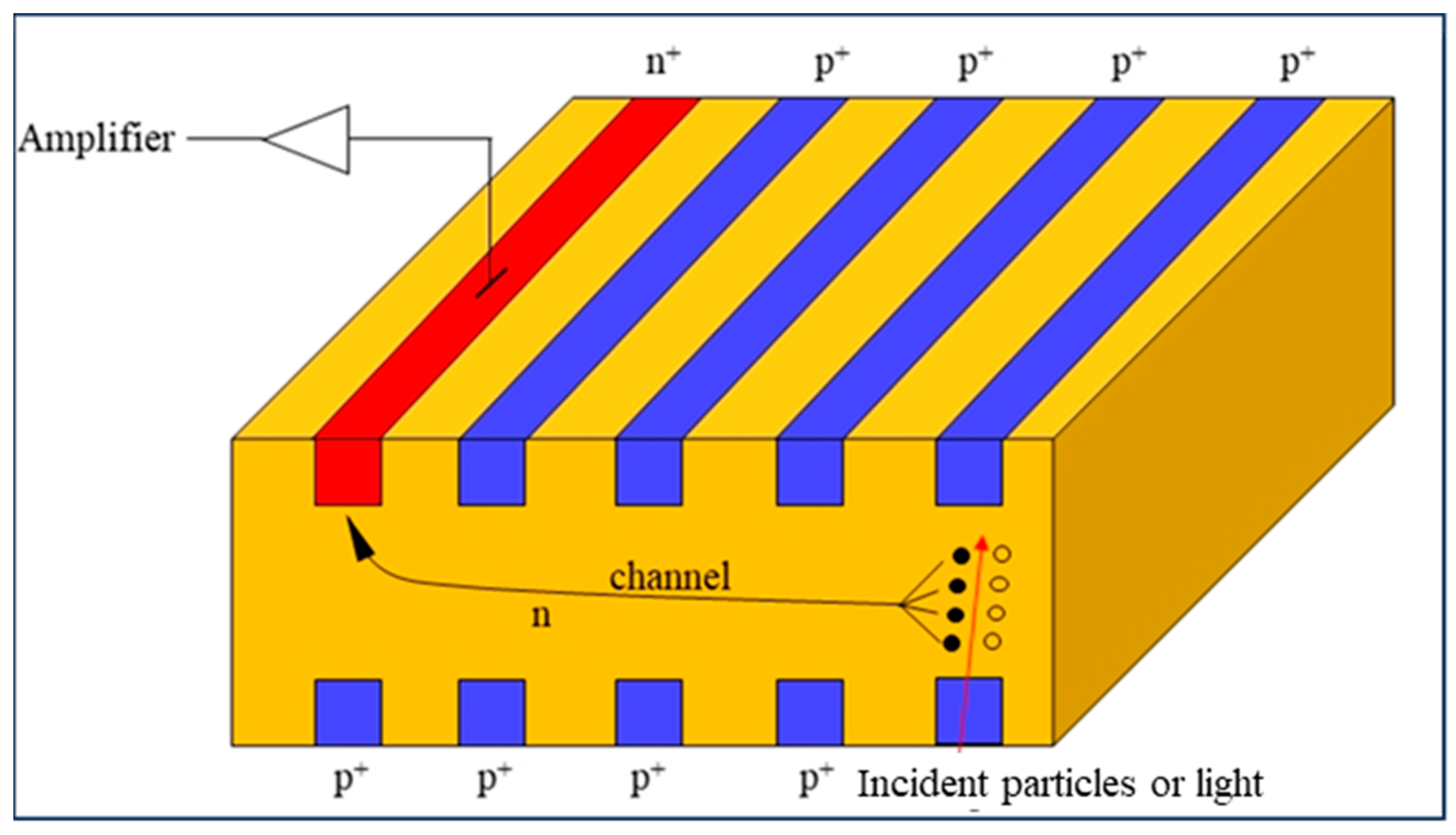
1. Introduction
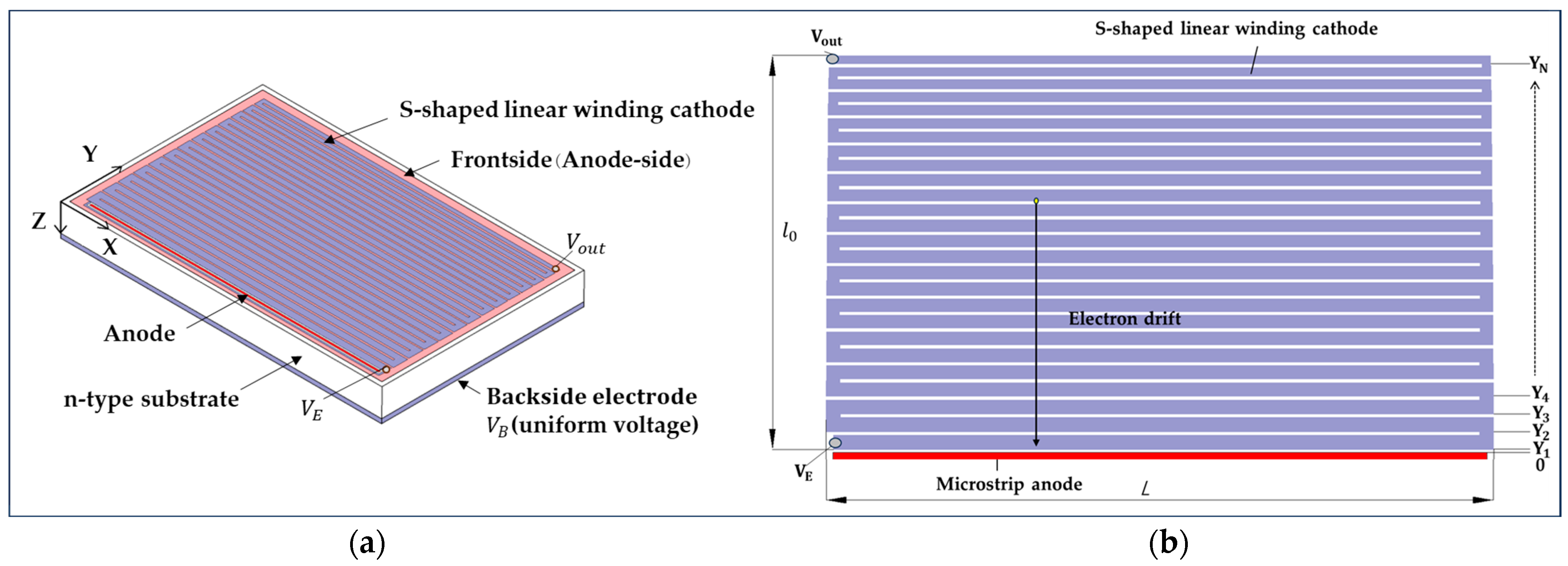
2. Design of the LWSDD Structure
2.1. Surface Field Profile in LWSDD—An Analytically Exact Solutions
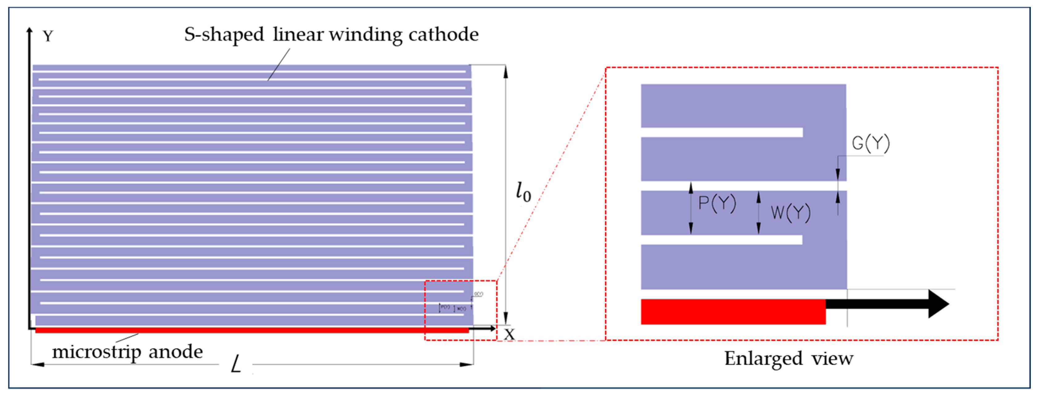
2.2. Linear Winding Electrode Design
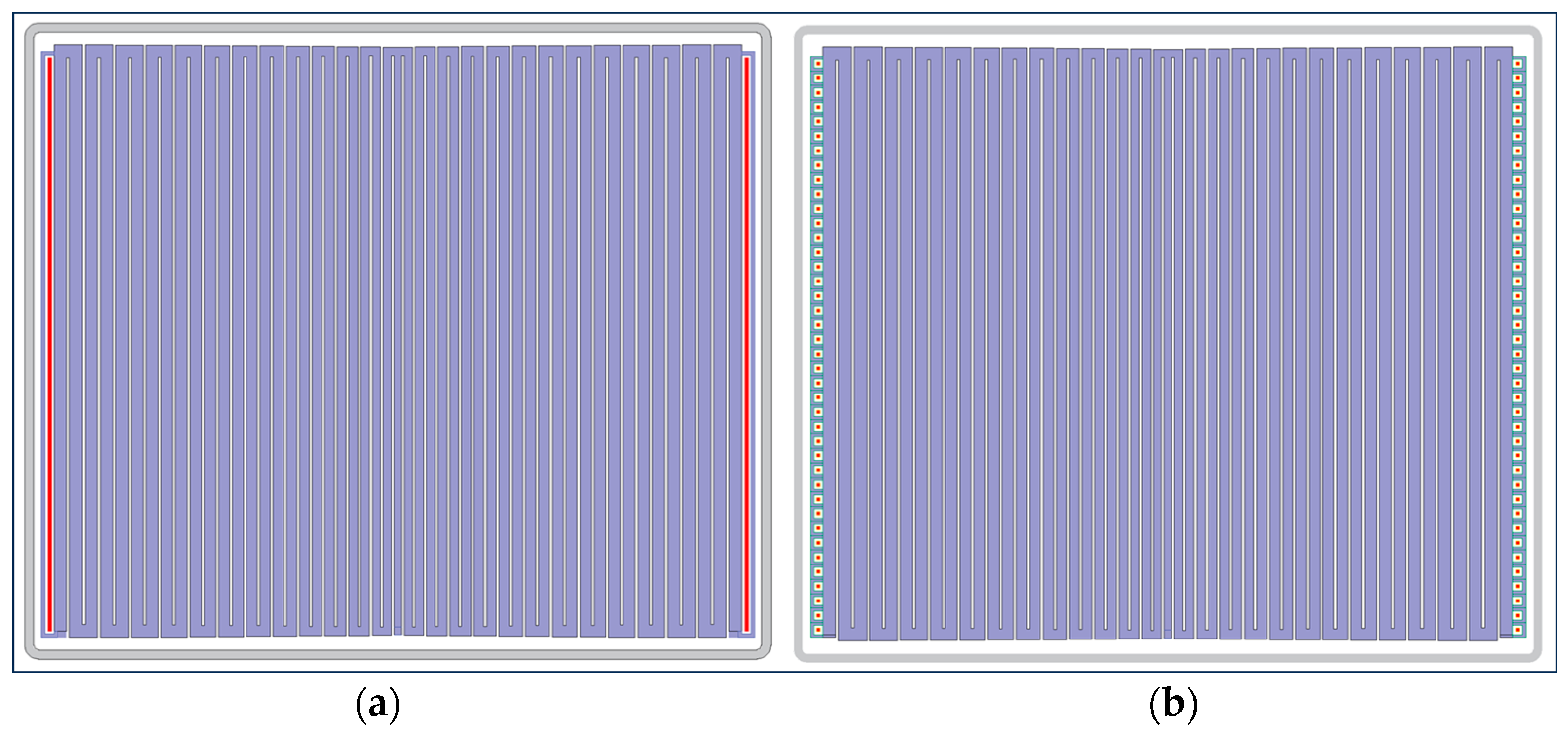
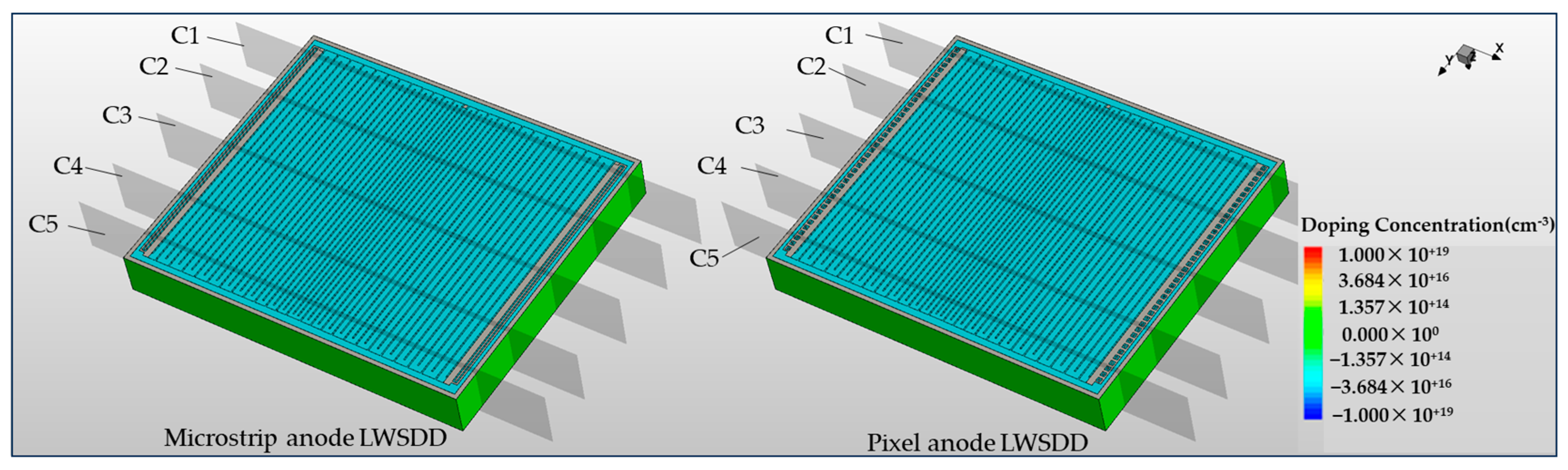
3. Modeling and 3D TCAD Simulation of LWSDD
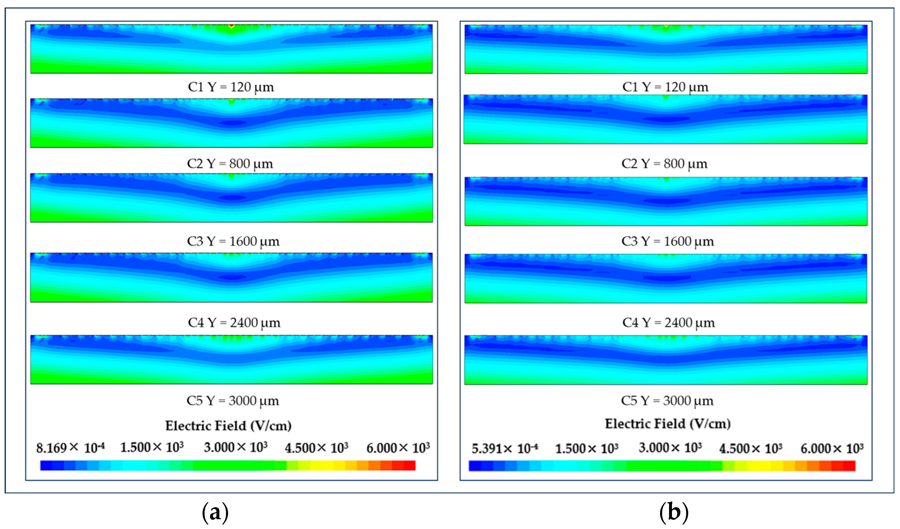
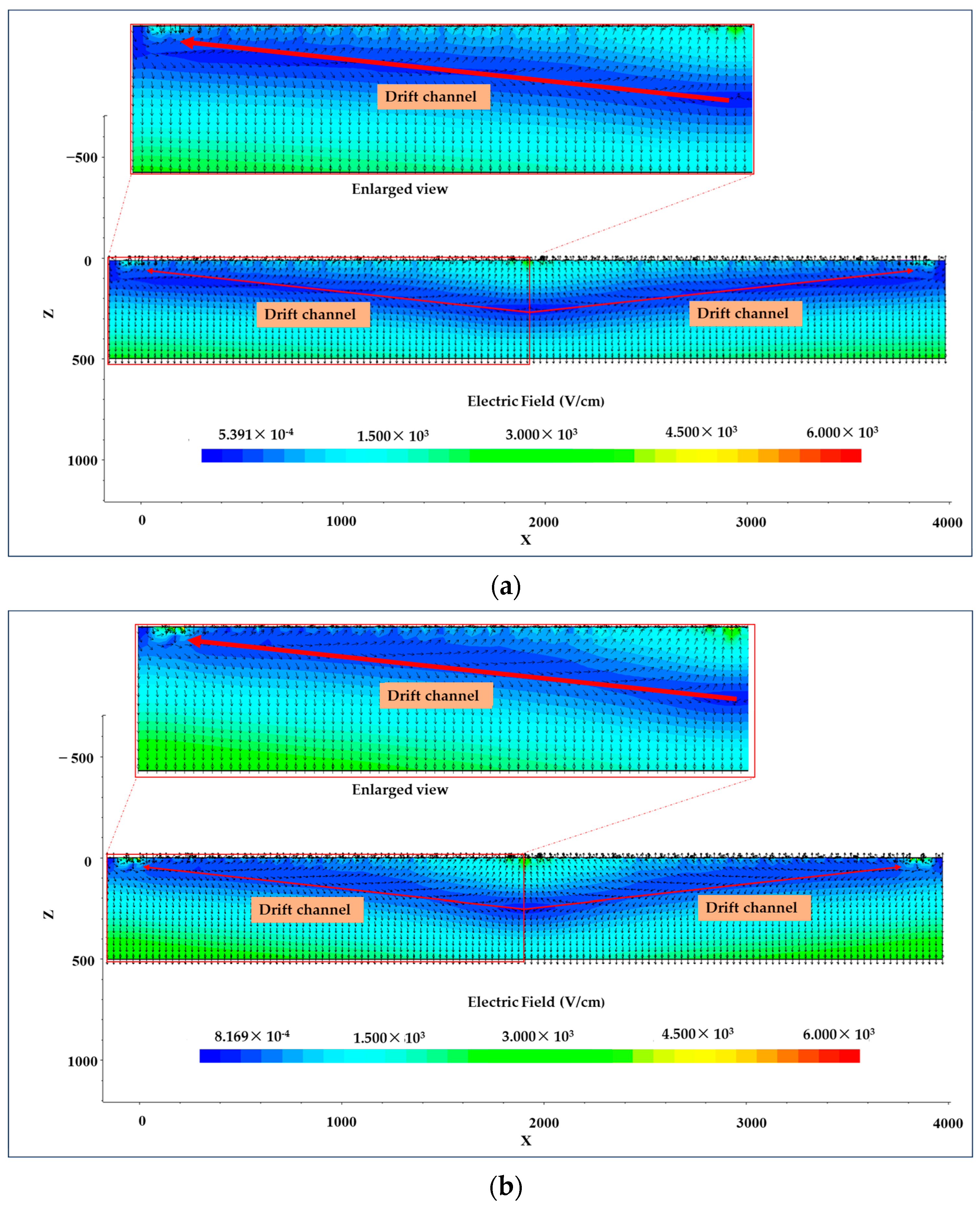
3.1. Electric Field Distribution of LWSDD
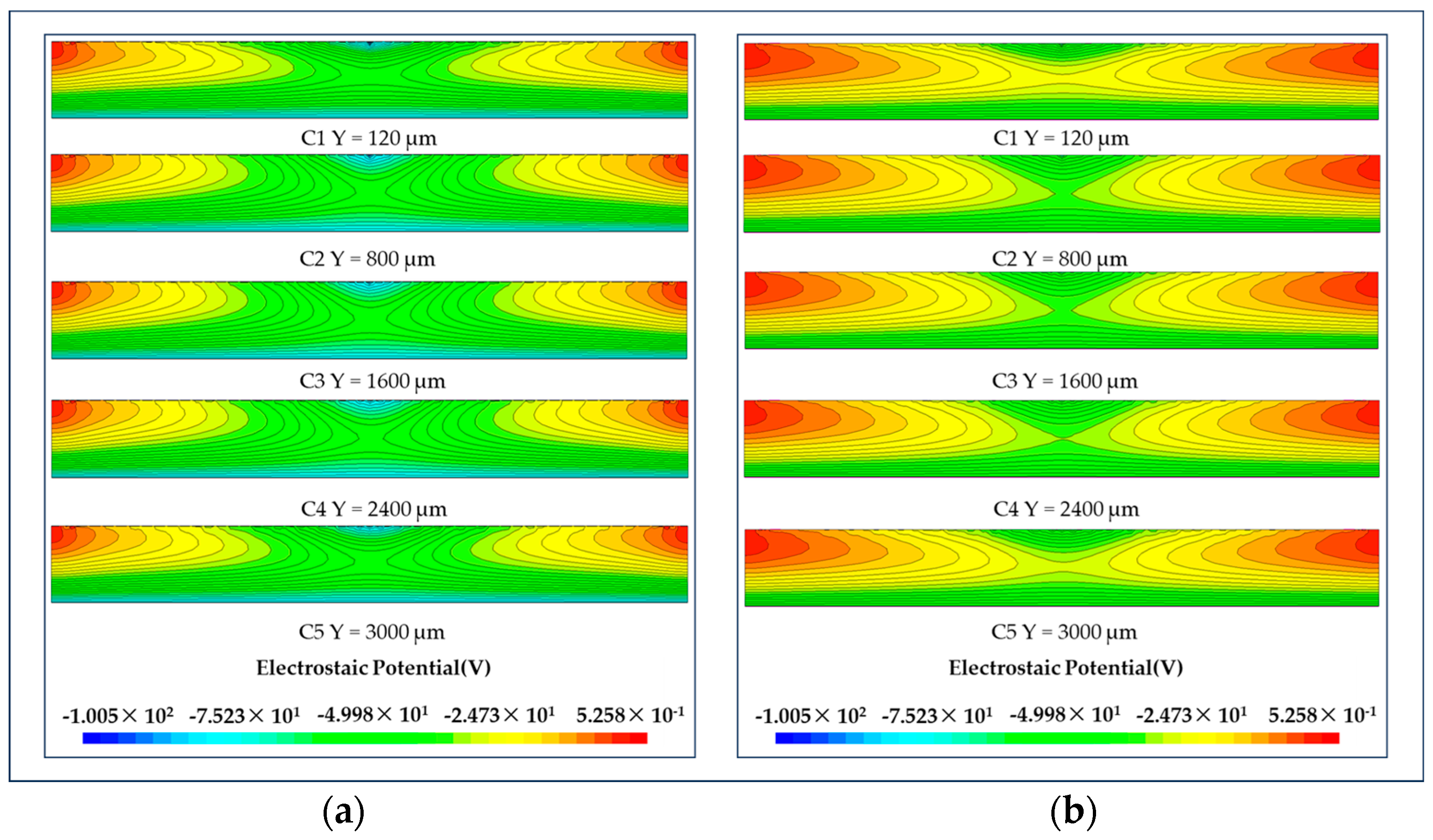
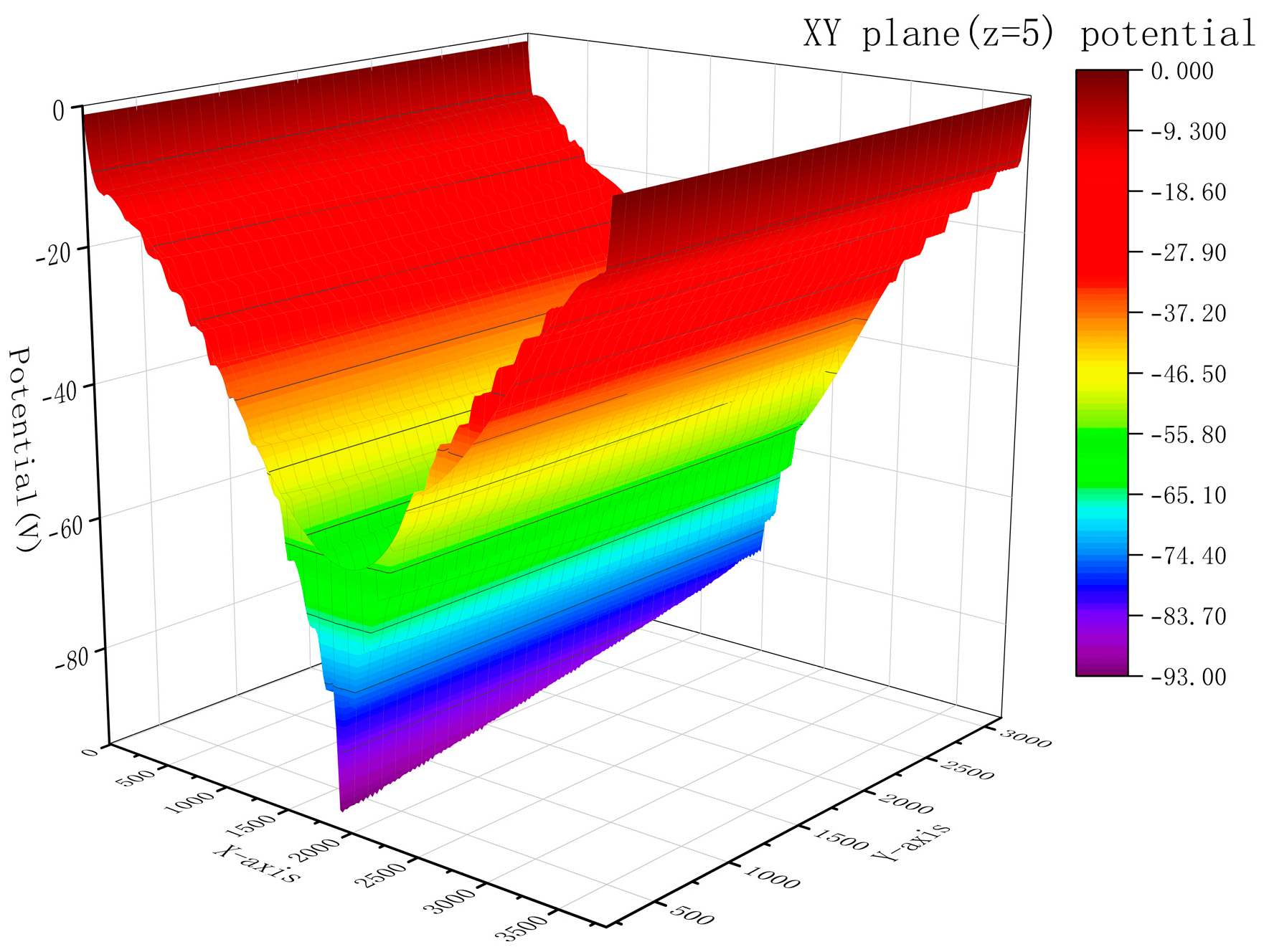
3.2. Potential Distribution of LWSDD
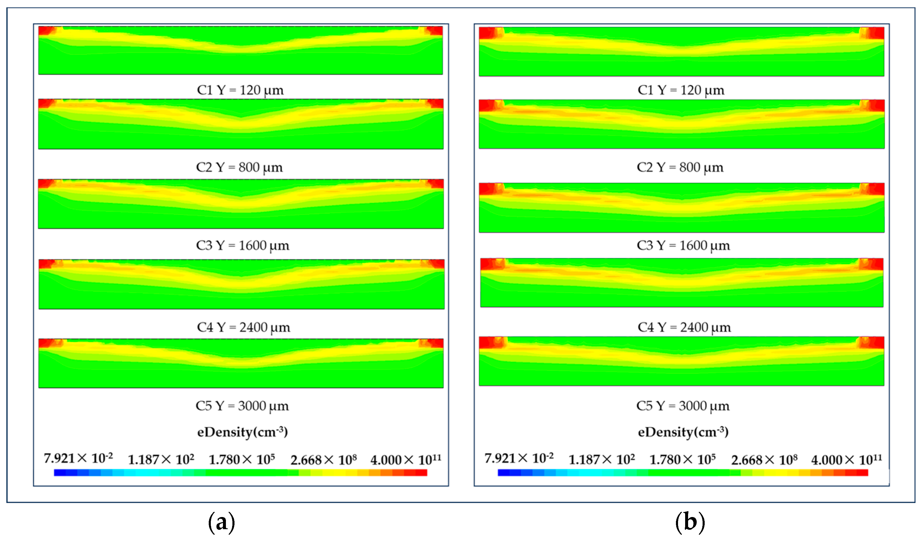
3.3. Electron Concentration Distribution of LWSDD
4. Conclusions
Author Contributions
Funding
Data Availability Statement
Conflicts of Interest
References
- Rehak, P.; Gatti, E.; Longoni, A.; Sampietro, M.; Holl, P. Spiral silicon drift detectors. IEEE Trans. Nucl. Sci 1989, 36, 203–209. [Google Scholar] [CrossRef]
- Mertens, S.; Brunst, T.; Korzeczek, M.; Lebert, M.; Siegmann, D.; Alborini, A.; Altenmüller, K.; Biassoni, M.; Bombelli, L.; Carminati, M. Characterization of silicon drift detectors with electrons for the TRISTAN project. J. Phys. G Nucl. Part. Phys. 2020, 48, 015008. [Google Scholar] [CrossRef]
- Miliucci, M.; Bazzi, M.; Bosnar, D.; Bragadireanu, M.; Carminati, M.; Cargnelli, M.; Clozza, A.; Curceanu, C.; Deda, G.; De Paolis, L. Silicon drift detectors’ spectroscopic response during the SIDDHARTA-2 kaonic helium run at the DAΦNE collider. Condens. Matter 2021, 6, 47. [Google Scholar] [CrossRef]
- Uematsu, Y.; Adamczyk, K.; Aggarwal, L.; Aihara, H.; Aziz, T.; Bacher, S.; Bahinipati, S.; Batignani, G.; Baudot, J.; Behera, P. The silicon vertex detector of the Belle II experiment. Nucl. Instrum. Methods Phys. Res. Sect. A Accel. Spectrom. Detect. Assoc. Equip. 2022, 1033, 166688. [Google Scholar] [CrossRef]
- Caputo, R.; Fukazawa, Y.; Johnson, R.; Longo, F.; Prest, M.; Tajima, H.; Vallazza, E. Silicon Detectors for Gamma-Ray Astronomy. In Handbook of X-ray and Gamma-ray Astrophysics; Springer: Berlin/Heidelberg, Germany, 2022; pp. 1–29. [Google Scholar]
- Cacciatore, F.; Ruiz, V.G.; Taubmann, G.; Muñoz, J.; Hermosín, P.; Sciarra, M.; Saco, M.; Rea, N.; Hernanz, M.; Parent, E. PODIUM: A Pulsar Navigation Unit for Science Missions. arXiv 2023, arXiv:2301.08744. [Google Scholar]
- Chen, W.; Giacomini, G.; Kuczewski, A.; Mead, J.; Rumaiz, A.; Siddons, D. Development of a large array of Silicon Drift Detectors for high-rate synchrotron fluorescence spectroscopy. J. Instrum. 2023, 18, P01016. [Google Scholar] [CrossRef]
- Cirrincione, D.; Antonelli, M.; Aquilanti, G.; Bellutti, P.; Bertuccio, G.; Borghi, G.; Cautero, G.; Ficorella, F.; Gandola, M.; Giuressi, D. A new collimated multichannel modular detection system based on Silicon Drift Detectors. Nucl. Instrum. Methods Phys. Res. Sect. A Accel. Spectrom. Detect. Assoc. Equip. 2023, 1049, 168118. [Google Scholar] [CrossRef]
- Di Giacomo, S.; Utica, G.; Carminati, M.; Borghi, G.; Picciotto, A.; Fiorini, C. Assessment of Silicon Drift Detector Timing Performance for Proton Therapy Application. In Proceedings of the 2021 IEEE Nuclear Science Symposium and Medical Imaging Conference (NSS/MIC), Virtual, 16–23 October 2021; pp. 1–4. [Google Scholar]
- Schilling, I.; Bäcker, C.M.; Bäumer, C.; Behrends, C.; Kröninger, K.; Timmermann, B.; Weingarten, J. Characterization of pixelated silicon detectors for daily quality assurance measurements in proton therapy. J. Phys. Conf. Ser. 2022, 2374, 012178. [Google Scholar] [CrossRef]
- Metzger, W.; Engdahl, J.; Rossner, W.; Boslau, O.; Kemmer, J. Large-area silicon drift detectors for new applications in nuclear medicine imaging. IEEE Trans. Nucl. Sci. 2004, 51, 1631–1635. [Google Scholar] [CrossRef]
- Biassoni, M.; Gugiatti, M.; Capelli, S.; Carminati, M.; Cremonesi, O.; Fiorini, C.; King, P.; Lechner, P.; Mertens, S.; Pagnanini, L. Electron spectrometry with Silicon drift detectors: A GEANT4 based method for detector response reconstruction. Eur. Phys. J. Plus 2021, 136, 125. [Google Scholar] [CrossRef]
- Gholami Hatam, E.; Pelicon, P.; Punzón-Quijorna, E.; Kelemen, M.; Vavpetič, P. Three-dimensional Element-by-element Surface Topography Reconstruction of Compound Samples Using Multisegment Silicon Drift Detectors. Microsc. Microanal. 2023, 29, 1980–1991. [Google Scholar] [CrossRef] [PubMed]
- Newbury, D.E.; Ritchie, N.W. Quantitative electron-excited X-ray microanalysis of borides, carbides, nitrides, oxides, and fluorides with scanning electron microscopy/silicon drift detector energy-dispersive spectrometry (SEM/SDD-EDS) and NIST DTSA-II. Microsc. Microanal. 2015, 21, 1327–1340. [Google Scholar] [CrossRef] [PubMed]
- Miliucci, M.; Iliescu, M.; Sgaramella, F.; Bazzi, M.; Bosnar, D.; Bragadireanu, M.; Carminati, M.; Cargnelli, M.; Clozza, A.; Curceanu, C. Large area silicon drift detectors system for high precision timed x-ray spectroscopy. Meas. Sci. Technol. 2022, 33, 095502. [Google Scholar] [CrossRef]
- Mu, S.; Rafaelsen, J.; Kawabata, M. SEM EDS Mapping of Ultra-Low Energy X-rays Using a Silicon Nitride Window Silicon Drift Detector. Microsc. Microanal. 2022, 28, 572–573. [Google Scholar] [CrossRef]
- Niculae, A.; Aschauer, S.; Bornschlegl, M.; Hermenau, K.; Heizinger, K.; Reinl, S.; Soltau, H.; Strüder, L. Latest Improvements on Silicon Drift Detectors for Fast, High Resolution EDX Spectroscopy in Electron Microscopy. Microsc Microanal. 2023, 29, 2087–2088. [Google Scholar] [CrossRef]
- Gatti, E.; Rehak, P. Semiconductor drift chamber—An application of a novel charge transport scheme. Nucl. Instrum. Methods Phys. Res. 1984, 225, 608–614. [Google Scholar] [CrossRef]
- Bellwied, R.; Beuttenmueller, R.; Chen, W.; DiMassimo, D.; Dou, L.; Dyke, H.; French, A.; Hall, J.; Hoffmann, G.; Humanic, T. Development of large linear silicon drift detectors for the STAR experiment at RHIC. Nucl. Instrum. Methods Phys. Res. Sect. A Accel. Spectrom. Detect. Assoc. Equip. 1996, 377, 387–392. [Google Scholar] [CrossRef]
- Li, Z. Generalization of the modeling and design considerations of concentric and spiral Si drift detectors. Nucl. Instrum. Methods Phys. Res. Sect. A Accel. Spectrom. Detect. Assoc. Equip. 2013, 730, 73–78. [Google Scholar] [CrossRef]


Disclaimer/Publisher’s Note: The statements, opinions and data contained in all publications are solely those of the individual author(s) and contributor(s) and not of MDPI and/or the editor(s). MDPI and/or the editor(s) disclaim responsibility for any injury to people or property resulting from any ideas, methods, instructions or products referred to in the content. |
© 2024 by the authors. Licensee MDPI, Basel, Switzerland. This article is an open access article distributed under the terms and conditions of the Creative Commons Attribution (CC BY) license (https://creativecommons.org/licenses/by/4.0/).
Share and Cite
Long, T.; Zhao, J.; Xiong, B.; Li, X.; Tang, M.; Li, Z. A Novel Position-Sensitive Linear Winding Silicon Drift Detector. Micromachines 2024, 15, 518. https://doi.org/10.3390/mi15040518
Long T, Zhao J, Xiong B, Li X, Tang M, Li Z. A Novel Position-Sensitive Linear Winding Silicon Drift Detector. Micromachines. 2024; 15(4):518. https://doi.org/10.3390/mi15040518
Chicago/Turabian StyleLong, Tao, Jun Zhao, Bo Xiong, Xinqing Li, Minghua Tang, and Zheng Li. 2024. "A Novel Position-Sensitive Linear Winding Silicon Drift Detector" Micromachines 15, no. 4: 518. https://doi.org/10.3390/mi15040518
APA StyleLong, T., Zhao, J., Xiong, B., Li, X., Tang, M., & Li, Z. (2024). A Novel Position-Sensitive Linear Winding Silicon Drift Detector. Micromachines, 15(4), 518. https://doi.org/10.3390/mi15040518