

The Effect of Height Error on Performance of Propagation Phase-Based Metalens


Abstract
1. Introduction
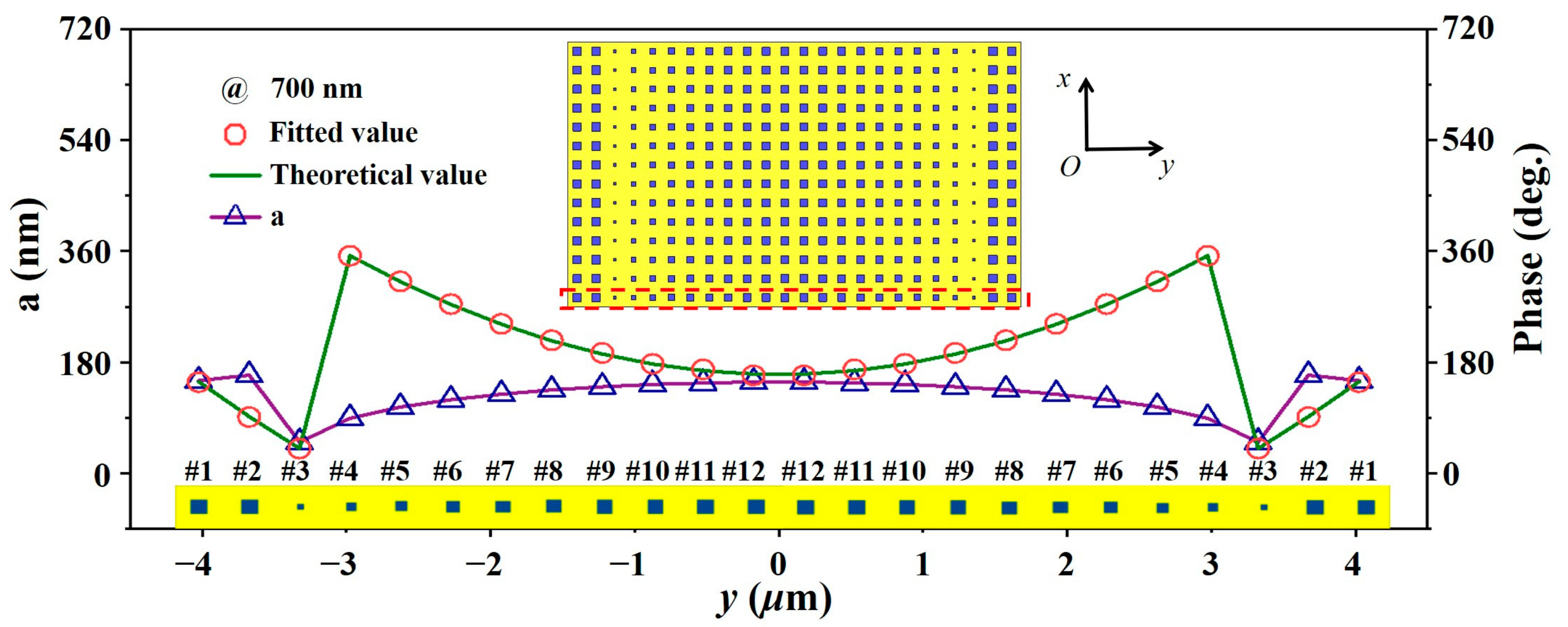
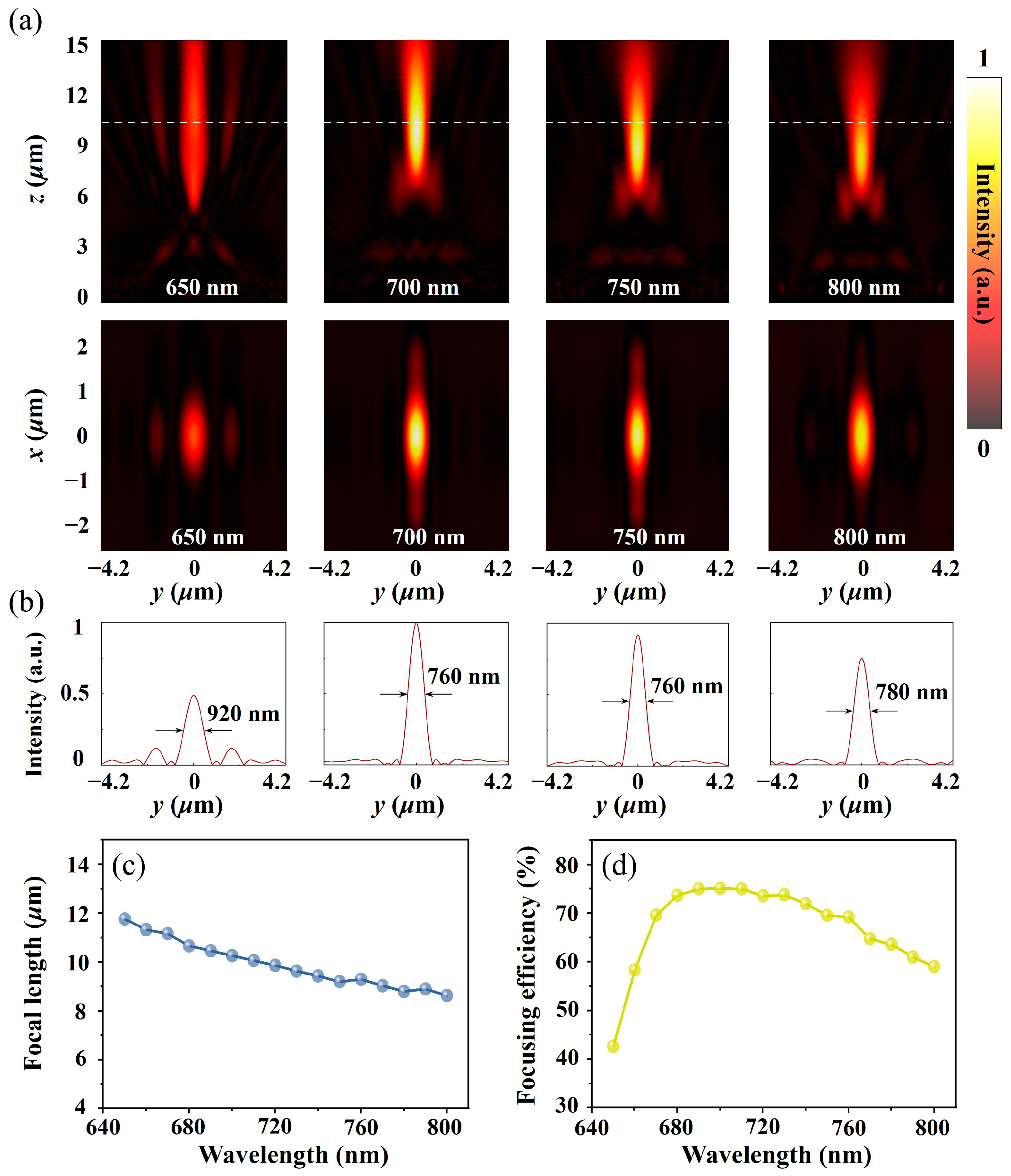
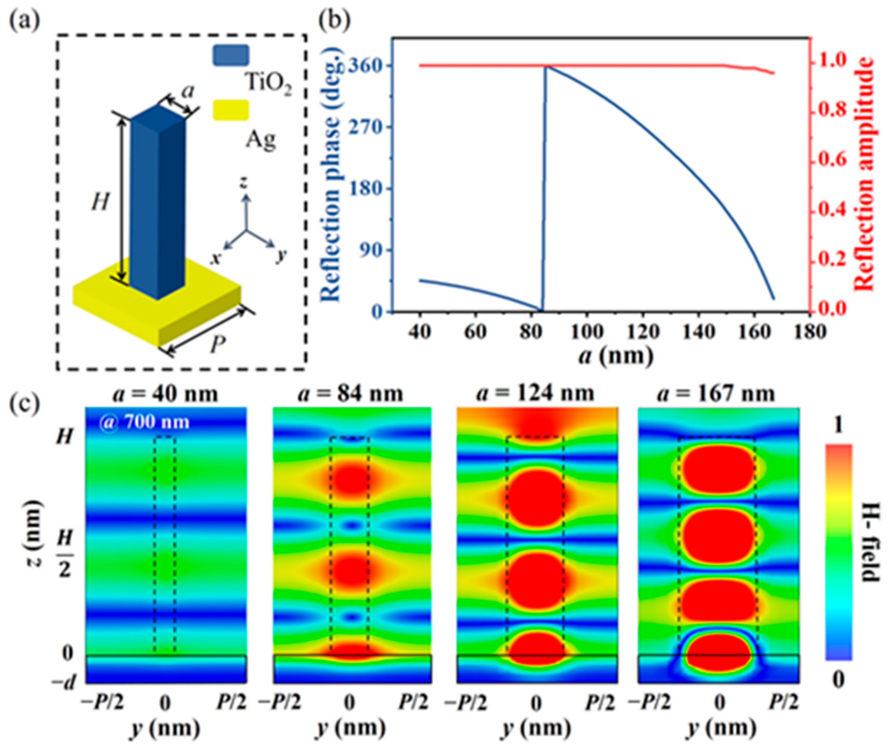
2. Metalens Design
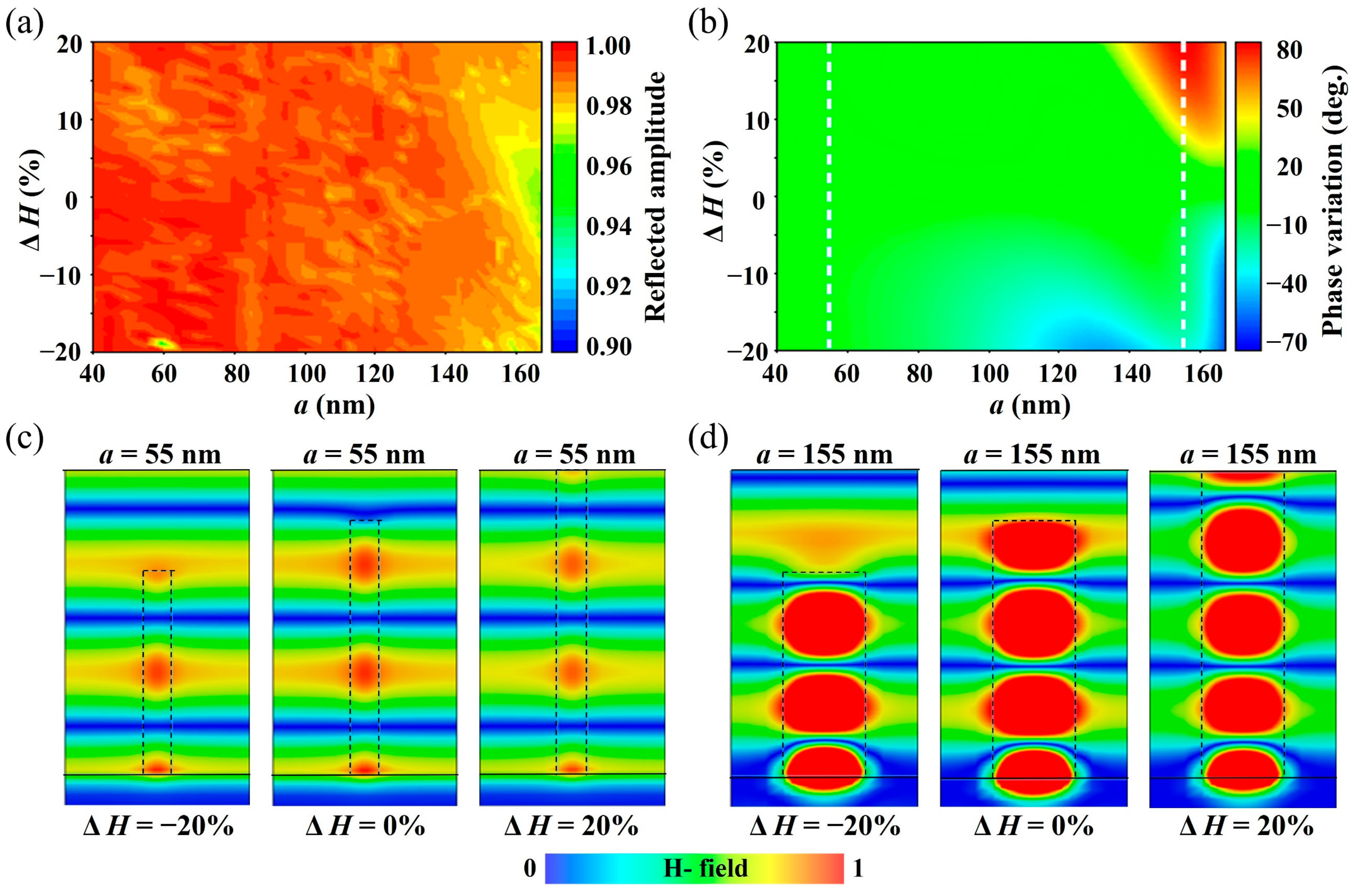
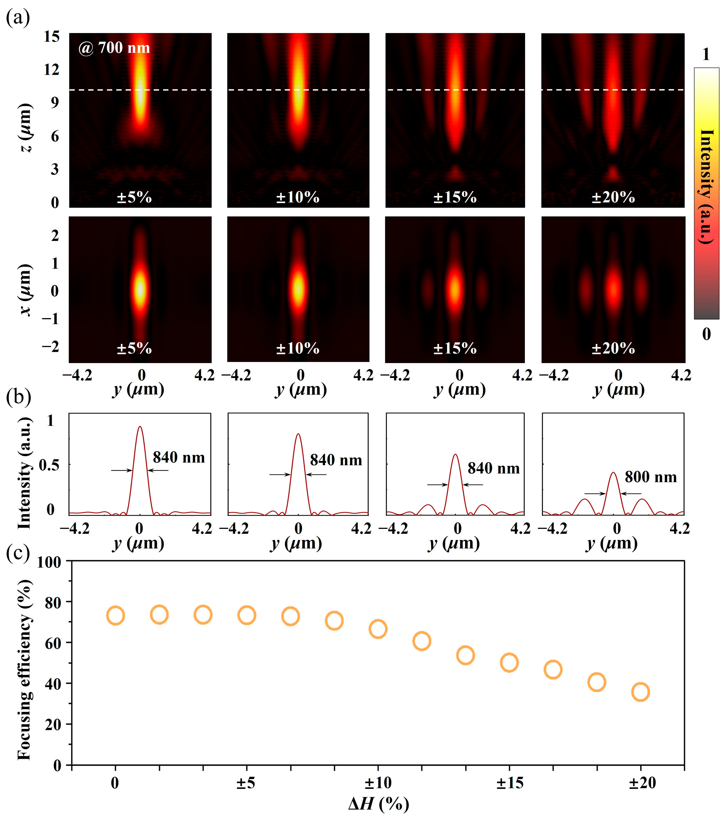
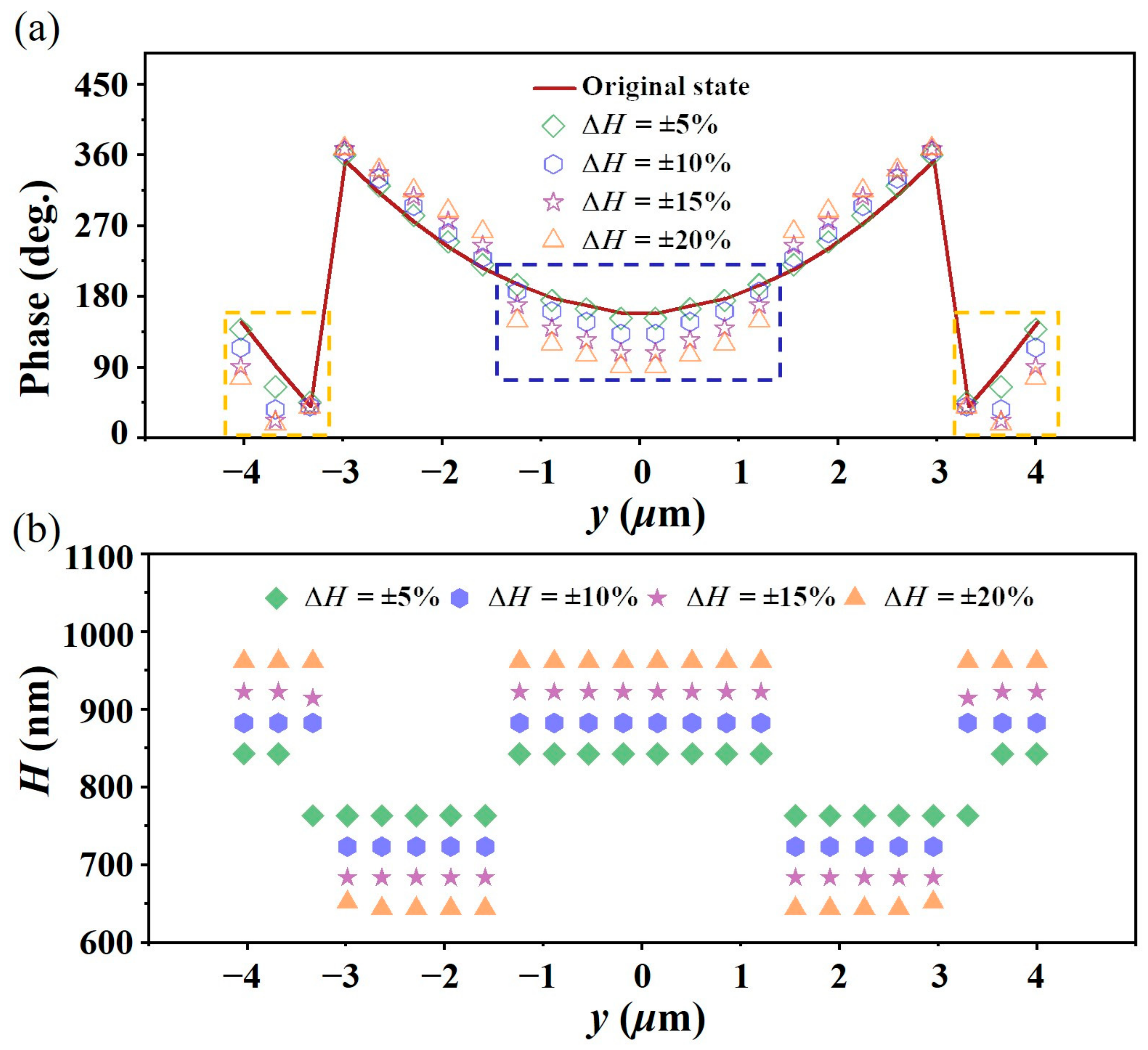
3. Error Analysis
4. Conclusions
Author Contributions
Funding
Data Availability Statement
Conflicts of Interest
References
- Deng, L.; Deng, J.; Guan, Z.; Tao, J.; Chen, Y.; Yang, Y.; Zhang, D.; Tang, J.; Li, Z.; Li, Z.; et al. Malus-Metasurface-Assisted Polarization Multiplexing. Light Sci. Appl. 2020, 9, 101. [Google Scholar] [CrossRef] [PubMed]
- Cheng, Q.; Wang, J.; Ma, L.; Shen, Z.; Zhang, J.; Zheng, X.; Chen, T.; Yu, Y.; Yu, D.; He, Q.; et al. Achromatic Terahertz Airy Beam Generation with Dielectric Metasurfaces. Nanophotonics 2021, 10, 1123–1131. [Google Scholar] [CrossRef]
- Deng, L.; Li, Z.; Zhou, Z.; He, Z.; Zeng, Y.; Zheng, G.; Yu, S. Bilayer-Metasurface Design, Fabrication, and Functionalization for Full-Space Light Manipulation. Adv. Opt. Mater. 2022, 10, 2102179. [Google Scholar] [CrossRef]
- Shi, T.; Deng, Z.-L.; Geng, G.; Zeng, X.; Zeng, Y.; Hu, G.; Overvig, A.; Li, J.; Qiu, C.-W.; Alù, A.; et al. Planar Chiral Metasurfaces with Maximal and Tunable Chiroptical Response Driven by Bound States in the Continuum. Nat. Commun. 2022, 13, 4111. [Google Scholar] [CrossRef] [PubMed]
- Wang, H.; Qin, Z.; Huang, L.; Li, Y.; Zhao, R.; Zhou, H.; He, H.; Zhang, J.; Qu, S. Metasurface with Dynamic Chiral Meta-Atoms for Spin Multiplexing Hologram and Low Observable Reflection. PhotoniX 2022, 3, 10. [Google Scholar] [CrossRef]
- Liu, F.; Wang, D.; Zhu, H.; Zhang, X.; Liu, T.; Sun, S.; Zhang, X.; He, Q.; Zhou, L. High-Efficiency Metasurface-Based Surface-Plasmon Lenses. Laser Photonics Rev. 2023, 17, 2201001. [Google Scholar] [CrossRef]
- Lee, D.; Gwak, J.; Badloe, T.; Palomba, S.; Rho, J. Metasurfaces-Based Imaging and Applications: From Miniaturized Optical Components to Functional Imaging Platforms. Nanoscale Adv. 2020, 2, 605–625. [Google Scholar] [CrossRef] [PubMed]
- Zhang, S.; Wong, C.L.; Zeng, S.; Bi, R.; Tai, K.; Dholakia, K.; Olivo, M. Metasurfaces for Biomedical Applications: Imaging and Sensing from a Nanophotonics Perspective. Nanophotonics 2020, 10, 259–293. [Google Scholar] [CrossRef]
- Zhao, X.; Sun, Z.; Zhang, L.; Wang, Z.; Xie, R.; Zhao, J.; You, R.; You, Z. Review on Metasurfaces: An Alternative Approach to Advanced Devices and Instruments. Adv. Devices Instrum. 2022, 2022, 9765089. [Google Scholar] [CrossRef]
- Ren, M.; Xu, J. Intelligent Metasurfaces Can Recognize Objects. Light Sci. Appl. 2022, 11, 211. [Google Scholar] [CrossRef]
- Qin, J.; Jiang, S.; Wang, Z.; Cheng, X.; Li, B.; Shi, Y.; Tsai, D.P.; Liu, A.Q.; Huang, W.; Zhu, W. Metasurface Micro/Nano-Optical Sensors: Principles and Applications. ACS Nano 2022, 16, 11598–11618. [Google Scholar] [CrossRef] [PubMed]
- Cortés, E.; Wendisch, F.J.; Sortino, L.; Mancini, A.; Ezendam, S.; Saris, S.; De SMenezes, L.; Tittl, A.; Ren, H.; Maier, S.A. Optical Metasurfaces for Energy Conversion. Chem. Rev. 2022, 122, 15082–15176. [Google Scholar] [CrossRef] [PubMed]
- Zheng, Y.; Chen, K.; Xu, Z.; Zhang, N.; Wang, J.; Zhao, J.; Feng, Y. Metasurface-Assisted Wireless Communication with Physical Level Information Encryption. Adv. Sci. 2022, 9, 2204558. [Google Scholar] [CrossRef] [PubMed]
- Zhang, C.; Zhan, Y.; Qiu, Y.; Xu, L.; Guan, J. Planar Metasurface-Based Concentrators for Solar Energy Harvest: From Theory to Engineering. PhotoniX 2022, 3, 28. [Google Scholar] [CrossRef]
- Lei, C.; Qian, M.; Si, L.S.; Ju, Y.F.; Yang, C.H.; Jun, C.T. Touch-Programmable Metasurface for Various Electromagnetic Manipulations and Encryptions (Small 45/2022). Small 2022, 18, 2203871. [Google Scholar]
- Ma, Q.; Gao, W.; Xiao, Q.; Ding, L.; Gao, T.; Zhou, Y.; Gao, X.; Yan, T.; Liu, C.; Gu, Z.; et al. Directly Wireless Communication of Human Minds via Non-Invasive Brain-Computer-Metasurface Platform. eLight 2022, 2, 11. [Google Scholar] [CrossRef]
- Chen, M.K.; Wu, Y.; Feng, L.; Fan, Q.; Lu, M.; Xu, T.; Tsai, D.P. Principles, Functions, and Applications of Optical Meta-Lens. Adv. Opt. Mater. 2021, 9, 2001414. [Google Scholar] [CrossRef]
- Wang, Y.; Chen, Q.; Yang, W.; Ji, Z.; Jin, L.; Ma, X.; Song, Q.; Boltasseva, A.; Han, J.; Shalaev, V.M.; et al. High-Efficiency Broadband Achromatic Metalens for near-IR Biological Imaging Window. Nat. Commun. 2021, 12, 5560. [Google Scholar] [CrossRef]
- Groever, B.; Chen, W.T.; Capasso, F. Meta-Lens Doublet in the Visible Region. Nano Lett. 2017, 17, 4902–4907. [Google Scholar] [CrossRef]
- Luo, X.; Zhang, F.; Pu, M.; Guo, Y.; Li, X.; Ma, X. Recent Advances of Wide-Angle Metalenses: Principle, Design, and Applications. Nanophotonics 2021, 11, 583. [Google Scholar] [CrossRef]
- Chen, W.T.; Zhu, A.Y.; Capasso, F. Flat Optics with Dispersion-Engineered Metasurfaces. Nat. Rev. Mater. 2020, 5, 604–620. [Google Scholar] [CrossRef]
- Fan, Z.-B.; Qiu, H.-Y.; Zhang, H.-L.; Pang, X.-N.; Zhou, L.-D.; Liu, L.; Ren, H.; Wang, Q.-H.; Dong, J.-W. A Broadband Achromatic Metalens Array for Integral Imaging in the Visible. Light Sci. Appl. 2019, 8, 67. [Google Scholar] [CrossRef] [PubMed]
- She, A.; Zhang, S.; Shian, S.; Clarke, D.R.; Capasso, F. Large Area Metalenses: Design, Characterization, and Mass Manufacturing. Opt. Express 2018, 26, 1573. [Google Scholar] [CrossRef]
- Ha, J.; Ndao, A.; Hsu, L.; Park, J.-H.; Kante, B. Planar Dielectric Cylindrical Lens at 800 Nm and the Role of Fabrication Imperfections. Opt. Express 2018, 26, 23178. [Google Scholar] [CrossRef]
- Brière, G.; Ni, P.; Héron, S.; Chenot, S.; Vézian, S.; Brändli, V.; Damilano, B.; Duboz, J.; Iwanaga, M.; Genevet, P. An Etching-Free Approach Toward Large-Scale Light-Emitting Metasurfaces. Adv. Opt. Mater. 2019, 7, 1801271. [Google Scholar] [CrossRef]
- Baracu, A.M.; Avram, M.A.; Breazu, C.; Bunea, M.-C.; Socol, M.; Stanculescu, A.; Matei, E.; Thrane, P.C.V.; Dirdal, C.A.; Dinescu, A.; et al. Silicon Metalens Fabrication from Electron Beam to UV-Nanoimprint Lithography. Nanomaterials 2021, 11, 2329. [Google Scholar] [CrossRef]
- Park, J.-S.; Lim, S.W.D.; Amirzhan, A.; Kang, H.; Karrfalt, K.; Kim, D.; Leger, J.; Urbas, A.; Ossiander, M.; Li, Z.; et al. All-Glass 100 Mm Diameter Visible Metalens for Imaging the Cosmos. ACS Nano 2024, 18, 3187–3198. [Google Scholar] [CrossRef]
- Lin, R.; Alnakhli, Z.; AlQatari, F.; Li, X. Analysis of Tapered Nanopillars for Reflective Metalens: The Role of Higher-Order Modes. IEEE Photonics J. 2020, 12, 1–7. [Google Scholar] [CrossRef]
- Zhou, Y.; Hu, T.; Li, Y.; Li, N.; Dong, Y.; Li, D.; Fu, Y.H.; Zhong, Q.; Xu, Z.; Zhu, S.; et al. A Performance Study of Dielectric Metalens with Process-Induced Defects. IEEE Photonics J. 2020, 12, 1–14. [Google Scholar] [CrossRef]
- Ma, X.; He, W.; Xin, L.; Yang, Z.; Liu, Z. Imaging Performance of a Mid-Infrared Metalens with a Machining Error. Appl. Opt. 2022, 61, 60. [Google Scholar] [CrossRef]
- Xu, G.; Kang, Q.; Fan, X.; Yang, G.; Guo, K.; Guo, Z. Influencing Effects of Fabrication Errors on Performances of the Dielectric Metalens. Micromachines 2022, 13, 2098. [Google Scholar] [CrossRef]
- Li, A.; Li, J.; Jia, H.; Duan, H.; Hu, Y. The Effect of Fabrication Error on the Performance of Mid-Infrared Metalens with Large Field-of-View. Nanomaterials 2023, 13, 440. [Google Scholar] [CrossRef] [PubMed]
- Ha, Y.; Lim, H.; Choi, H.; Lee, J. Fabrication of Nanostructures on a Large-Area Substrate with a Minimized Stitch Error Using the Step-and-Repeat Nanoimprint Process. Materials 2022, 15, 6036. [Google Scholar] [CrossRef]
- Ji, R.; Hornung, M.; Verschuuren, M.A.; Van De Laar, R.; Van Eekelen, J.; Plachetka, U.; Moeller, M.; Moormann, C. UV Enhanced Substrate Conformal Imprint Lithography (UV-SCIL) Technique for Photonic Crystals Patterning in LED Manufacturing. Microelectron. Eng. 2010, 87, 963–967. [Google Scholar] [CrossRef]
- Li, N.; Xu, Z.; Dong, Y.; Hu, T.; Zhong, Q.; Fu, Y.H.; Zhu, S.; Singh, N. Large-Area Metasurface on CMOS-Compatible Fabrication Platform: Driving Flat Optics from Lab to Fab. Nanophotonics 2020, 9, 3071–3087. [Google Scholar] [CrossRef]
- Park, J.-S.; Zhang, S.; She, A.; Chen, W.T.; Lin, P.; Yousef, K.M.A.; Cheng, J.-X.; Capasso, F. All-Glass, Large Metalens at Visible Wavelength Using Deep-Ultraviolet Projection Lithography. Nano Lett. 2019, 19, 8673–8682. [Google Scholar] [CrossRef] [PubMed]
- Elers, K.-E.; Blomberg, T.; Peussa, M.; Aitchison, B.; Haukka, S.; Marcus, S. Film Uniformity in Atomic Layer Deposition. Chem. Vap. Depos. 2006, 12, 13–24. [Google Scholar] [CrossRef]
- Jenkins, R.P.; Campbell, S.D.; Werner, D.H. Establishing Exhaustive Metasurface Robustness against Fabrication Uncertainties through Deep Learning. Nanophotonics 2021, 10, 4497–4509. [Google Scholar] [CrossRef]
- Mao, L.; Geng, Y.; Cao, Y.; Yan, Y. Uniform High-Reflectivity Silver Film Deposited by Planar Magnetron Sputtering. Vacuum 2021, 185, 109999. [Google Scholar] [CrossRef]
- Wu, B.; Kumar, A.; Pamarthy, S. High Aspect Ratio Silicon Etch: A Review. J. Appl. Phys. 2010, 108, 051101. [Google Scholar] [CrossRef]
- Biswas, A.; Pawar, V.S.; Menon, P.K.; Pal, P.; Pandey, A.K. Influence of Fabrication Tolerances on Performance Characteristics of a MEMS Gyroscope. Microsyst. Technol. 2021, 27, 2679–2693. [Google Scholar] [CrossRef]
- DeVore, J.R. Refractive Indices of Rutile and Sphalerite. J. Opt. Soc. Am. 1951, 41, 416. [Google Scholar] [CrossRef]
- Alù, A.; Salandrino, A.; Engheta, N. Negative Effective Permeability and Left-Handed Materials at Optical Frequencies. Opt. Express 2006, 14, 1557. [Google Scholar] [CrossRef]
- Yu, N.; Genevet, P.; Kats, M.A.; Aieta, F.; Tetienne, J.-P.; Capasso, F.; Gaburro, Z. Light Propagation with Phase Discontinuities: Generalized Laws of Reflection and Refraction. Science 2011, 334, 333–337. [Google Scholar] [CrossRef] [PubMed]
- Wang, S.; Wu, P.C.; Su, V.-C.; Lai, Y.-C.; Hung Chu, C.; Chen, J.-W.; Lu, S.-H.; Chen, J.; Xu, B.; Kuan, C.-H.; et al. Broadband Achromatic Optical Metasurface Devices. Nat. Commun. 2017, 8, 187. [Google Scholar] [CrossRef] [PubMed]
- Khorasaninejad, M.; Shi, Z.; Zhu, A.Y.; Chen, W.T.; Sanjeev, V.; Zaidi, A.; Capasso, F. Achromatic Metalens over 60 Nm Bandwidth in the Visible and Metalens with Reverse Chromatic Dispersion. Nano Lett. 2017, 17, 1819–1824. [Google Scholar] [CrossRef] [PubMed]
- Shi, Z.; Khorasaninejad, M.; Huang, Y.-W.; Roques-Carmes, C.; Zhu, A.Y.; Chen, W.T.; Sanjeev, V.; Ding, Z.-W.; Tamagnone, M.; Chaudhary, K.; et al. Single-Layer Metasurface with Controllable Multiwavelength Functions. Nano Lett. 2018, 18, 2420–2427. [Google Scholar] [CrossRef] [PubMed]
- Kamali, S.M.; Arbabi, A.; Arbabi, E.; Horie, Y.; Faraon, A. Decoupling Optical Function and Geometrical Form Using Conformal Flexible Dielectric Metasurfaces. Nat. Commun. 2016, 7, 11618. [Google Scholar] [CrossRef] [PubMed]
- Wang, S.; Wu, P.C.; Su, V.-C.; Lai, Y.-C.; Chen, M.-K.; Kuo, H.Y.; Chen, B.H.; Chen, Y.H.; Huang, T.-T.; Wang, J.-H.; et al. A Broadband Achromatic Metalens in the Visible. Nat. Nanotech. 2018, 13, 227–232. [Google Scholar] [CrossRef]
- Yang, Y.; Miroshnichenko, A.E.; Kostinski, S.V.; Odit, M.; Kapitanova, P.; Qiu, M.; Kivshar, Y.S. Multimode Directionality in All-Dielectric Metasurfaces. Phys. Rev. B 2017, 95, 165426. [Google Scholar] [CrossRef]


| ΔH | ±5% | ±10% | ±15% | ±20% | |
|---|---|---|---|---|---|
| No. | |||||
| #1 | −12.29 | −35.72 | −60.34 | −74.93 | |
| #2 | −29.57 | −58.46 | −72.66 | −77.10 | |
| #3 | 1.63 | −3.23 | −3.76 | −4.25 | |
| #4 | 5.93 | 10.96 | 13.80 | 14.50 | |
| #5 | 7.88 | 17.39 | 24.61 | 28.27 | |
| #6 | 6.96 | 19.05 | 30.77 | 38.91 | |
| #7 | 4.99 | 16.28 | 31.26 | 44.78 | |
| #8 | 2.59 | 11.57 | 27.09 | 44.99 | |
| #9 | −2.59 | −11.40 | −28.60 | −48.85 | |
| #10 | −5.13 | −18.92 | −40.61 | −60.65 | |
| #11 | −6.89 | −23.68 | −47.08 | −65.93 | |
| #12 | −9.27 | −29.17 | −53.61 | −70.63 | |
Disclaimer/Publisher’s Note: The statements, opinions and data contained in all publications are solely those of the individual author(s) and contributor(s) and not of MDPI and/or the editor(s). MDPI and/or the editor(s) disclaim responsibility for any injury to people or property resulting from any ideas, methods, instructions or products referred to in the content. |
© 2024 by the authors. Licensee MDPI, Basel, Switzerland. This article is an open access article distributed under the terms and conditions of the Creative Commons Attribution (CC BY) license (https://creativecommons.org/licenses/by/4.0/).
Share and Cite
Qiu, Y.; Deng, L.; Zhan, Y.; Li, G.; Guan, J. The Effect of Height Error on Performance of Propagation Phase-Based Metalens. Micromachines 2024, 15, 540. https://doi.org/10.3390/mi15040540
Qiu Y, Deng L, Zhan Y, Li G, Guan J. The Effect of Height Error on Performance of Propagation Phase-Based Metalens. Micromachines. 2024; 15(4):540. https://doi.org/10.3390/mi15040540
Chicago/Turabian StyleQiu, Yongxue, Liangui Deng, Yujie Zhan, Gongfa Li, and Jianguo Guan. 2024. "The Effect of Height Error on Performance of Propagation Phase-Based Metalens" Micromachines 15, no. 4: 540. https://doi.org/10.3390/mi15040540
APA StyleQiu, Y., Deng, L., Zhan, Y., Li, G., & Guan, J. (2024). The Effect of Height Error on Performance of Propagation Phase-Based Metalens. Micromachines, 15(4), 540. https://doi.org/10.3390/mi15040540