
Dependence of a Hydrogen Buffer Layer on the Properties of Top-Gate IGZO TFT


Abstract
1. Introduction
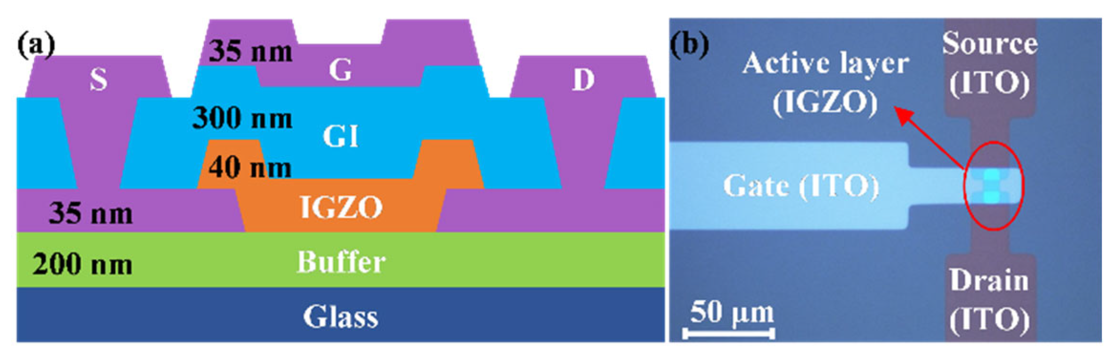
2. Experiment
3. Results and Discussion
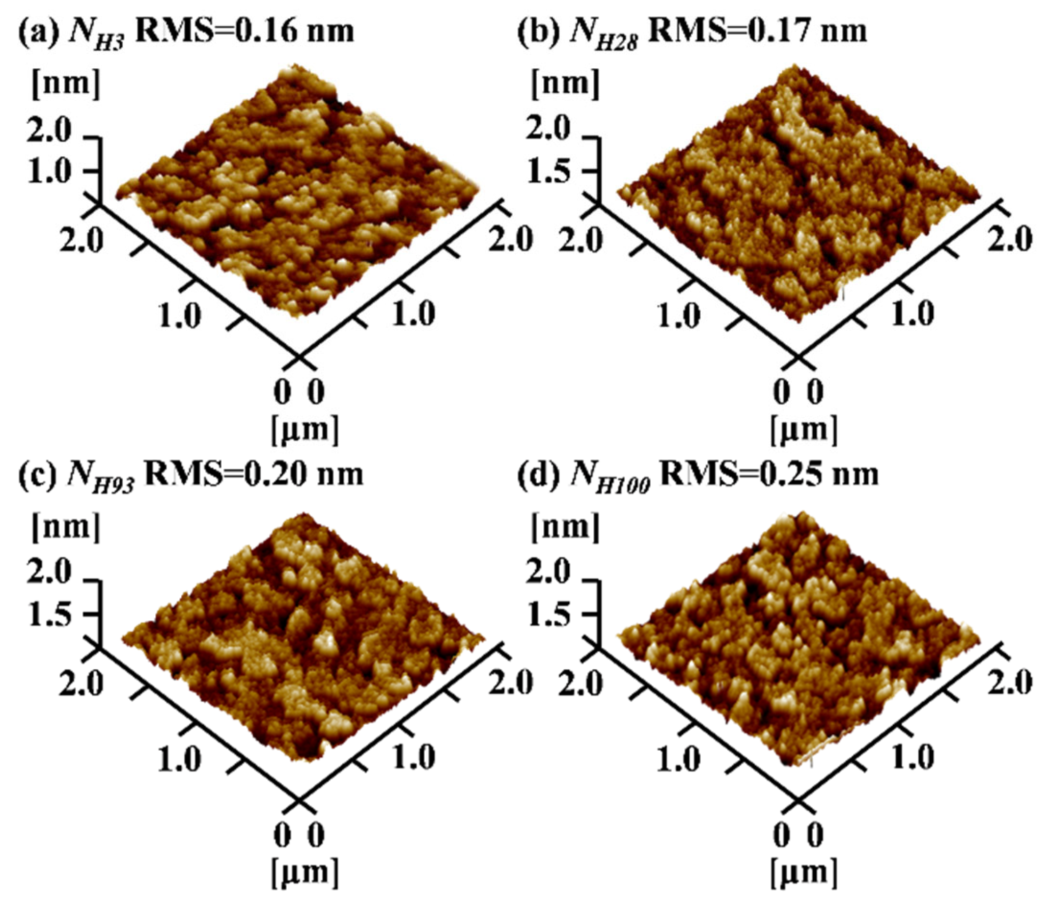
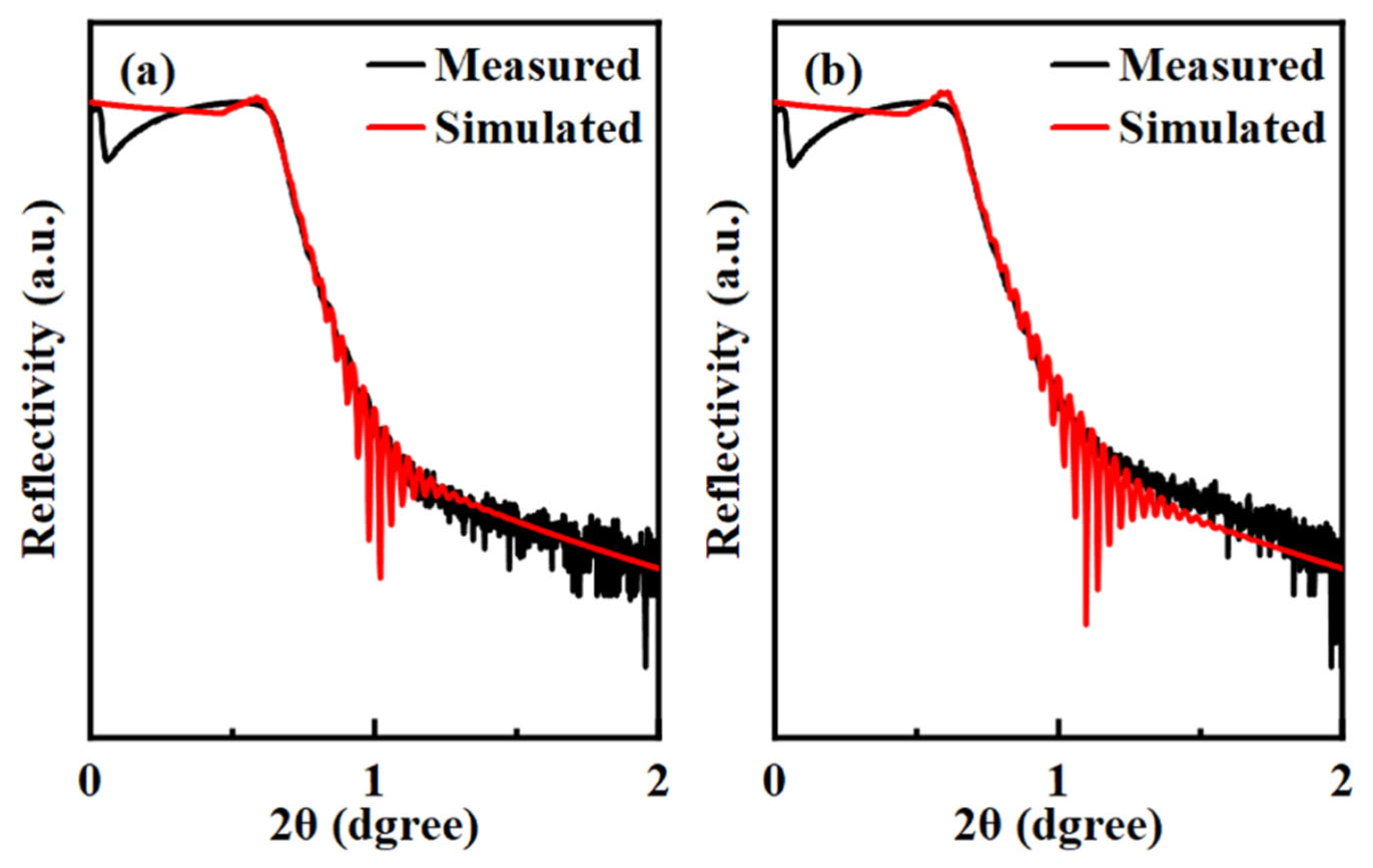
3.1. Thin-Film Performance Analysis
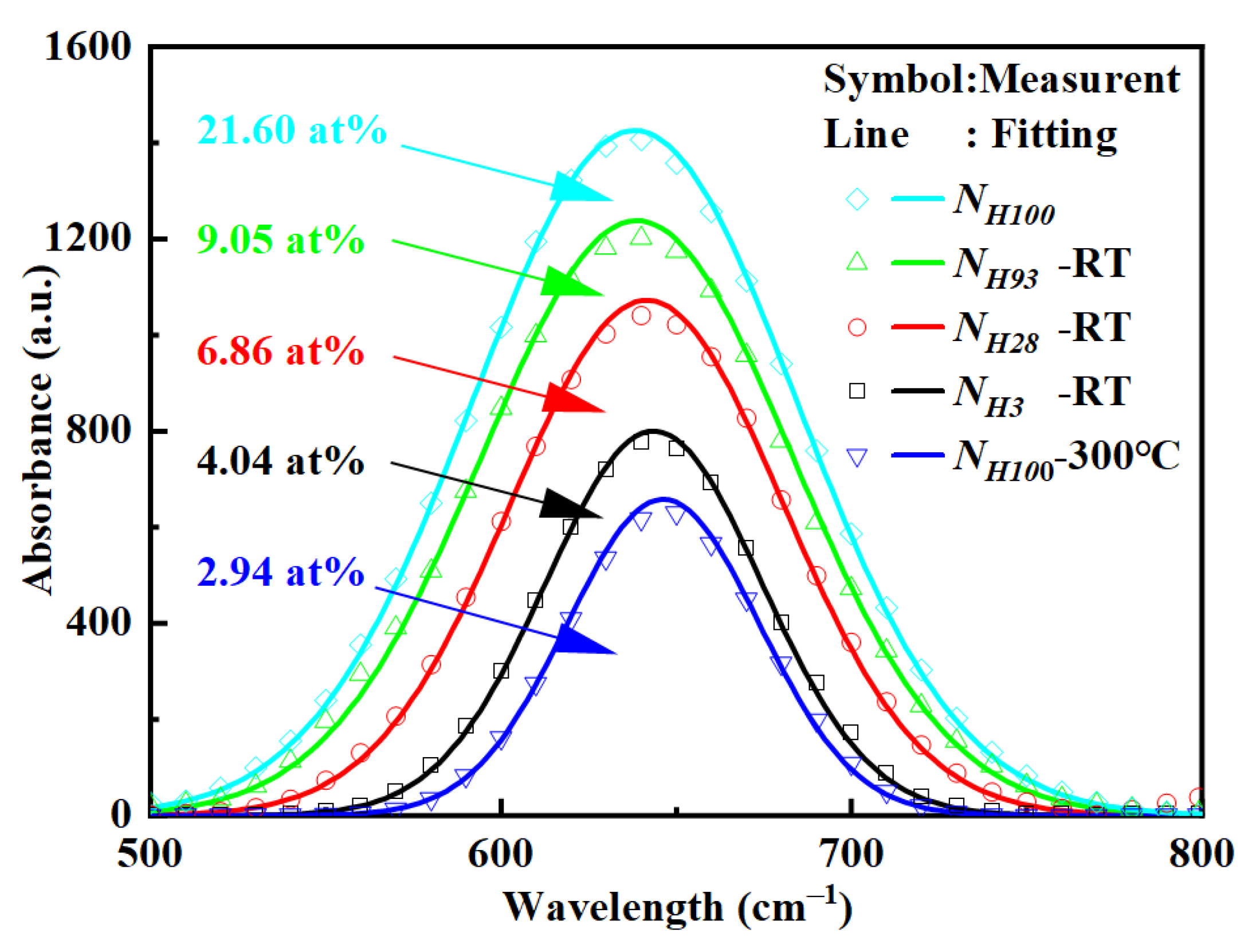
3.2. The Influence of Hydrogen Content in the Buffer Layer
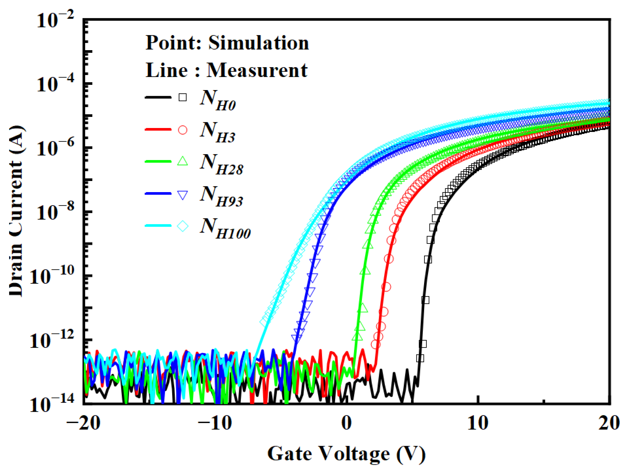
3.3. 2D Numerical Simulation
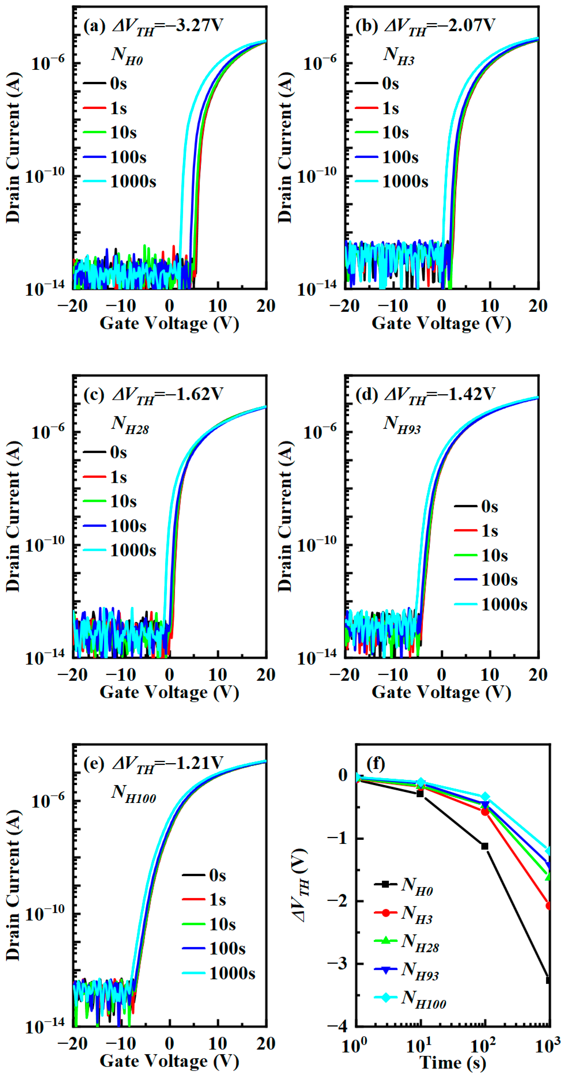
3.4. The Influence of Hydrogen Content on Stability
4. Conclusions
Author Contributions
Funding
Data Availability Statement
Conflicts of Interest
References
- Park, J.C.; Ahn, S.-E.; Lee, H.-N. High-Performance Low-Cost Back-Channel-Etch Amorphous Gallium–Indium–Zinc Oxide Thin-Film Transistors by Curing and Passivation of the Damaged Back Channel. ACS Appl. Mater. Interfaces 2013, 5, 12262–12267. [Google Scholar] [CrossRef] [PubMed]
- Han, K.-L.; Ok, K.-C.; Cho, H.-S.; Oh, S.; Park, J.-S. Effect of Hydrogen on the Device Performance and Stability Characteristics of Amorphous InGaZnO Thin-Film Transistors with a SiO2/SiNx/SiO2 Buffer. Appl. Phys. Lett. 2017, 111, 063502. [Google Scholar] [CrossRef]
- Peng, C.; Yang, S.; Pan, C.; Li, X.; Zhang, J. Effect of Two-Step Annealing on High Stability of a-IGZO Thin-Film Transistor. IEEE Trans. Electron. Devices 2020, 67, 4262–4268. [Google Scholar] [CrossRef]
- Zhang, Y.; He, G.; Wang, L.; Wang, W.; Xu, X.; Liu, W. Ultraviolet-Assisted Low-Thermal-Budget-Driven α-InGaZnO Thin Films for High-Performance Transistors and Logic Circuits. ACS Nano 2022, 16, 4961–4971. [Google Scholar] [CrossRef] [PubMed]
- Peng, C.; Xu, M.; Chen, L.; Li, X.; Zhang, J. Improvement of Properties of Top-Gate IGZO TFT by Oxygen-Rich Ultrathin in Situ ITO Active Layer. Jpn. J. Appl. Phys. 2022, 61, 070914. [Google Scholar] [CrossRef]
- Lin, D.; Su, W.-C.; Chang, T.-C.; Chen, H.-C.; Tu, Y.-F.; Zhou, K.-J.; Hung, Y.-H.; Yang, J.; Lu, I.-N.; Tsai, T.-M. Degradation Behavior of Etch-Stopper-Layer Structured a-InGaZnO Thin-Film Transistors under Hot-Carrier Stress and Illumination. IEEE Trans. Electron. Devices 2021, 68, 556–559. [Google Scholar] [CrossRef]
- Song, A.; Hong, H.M.; Son, K.S.; Lim, J.H.; Chung, K.-B. Hydrogen Behavior in Top Gate Amorphous In-Ga-Zn-O Device Fabrication Process during Gate Insulator Deposition and Gate Insulator Etching. IEEE Trans. Electron. Devices 2021, 68, 2723–2728. [Google Scholar] [CrossRef]
- Fakhri, M.; Theisen, M.; Behrendt, A.; Görrn, P.; Riedl, T. Top-Gate Zinc Tin Oxide Thin-Film Transistors with High Bias and Environmental Stress Stability. Appl. Phys. Lett. 2014, 104, 251603. [Google Scholar] [CrossRef]
- Lee, M.-X.; Chiu, J.-C.; Li, S.-L.; Sarkar, E.; Chen, Y.-C.; Yen, C.-C.; Chen, T.-L.; Chou, C.-H.; Liu, C. Mobility Enhancement and Abnormal Humps in Top-Gate Self-Aligned Double-Layer Amorphous InGaZnO TFTs. IEEE J. Electron. Devices Soc. 2022, 10, 301–308. [Google Scholar] [CrossRef]
- Hong, S.-Y.; Kim, H.-J.; Kim, D.-H.; Jeong, H.-Y.; Song, S.-H.; Cho, I.-T.; Noh, J.; Yun, P.S.; Lee, S.-W.; Park, K.-S. Study on the Lateral Carrier Diffusion and Source-Drain Series Resistance in Self-Aligned Top-Gate Coplanar InGaZnO Thin-Film Transistors. Sci. Rep. 2019, 9, 6588. [Google Scholar] [CrossRef]
- Chen, H.-C.; Chen, G.-F.; Chen, P.-H.; Huang, S.-P.; Chen, J.-J.; Zhou, K.-J.; Kuo, C.-W.; Tsao, Y.-C.; Chu, A.-K.; Huang, H.-C. A Novel Heat Dissipation Structure for Inhibiting Hydrogen Diffusion in Top-Gate a-InGaZnO TFTs. IEEE Electron. Device Lett. 2019, 40, 1447–1450. [Google Scholar] [CrossRef]
- Petti, L.; Münzenrieder, N.; Vogt, C.; Faber, H.; Büthe, L.; Cantarella, G.; Bottacchi, F.; Anthopoulos, T.D.; Tröster, G. Metal Oxide Semiconductor Thin-Film Transistors for Flexible Electronics. Appl. Phys. Rev. 2016, 3, 021303. [Google Scholar] [CrossRef]
- Han, K.-L.; Han, J.-H.; Kim, B.-S.; Jeong, H.-J.; Choi, J.-M.; Hwang, J.-E.; Oh, S.; Park, J.-S. Organic/Inorganic Hybrid Buffer in InGaZnO Transistors under Repetitive Bending Stress for High Electrical and Mechanical Stability. ACS Appl. Mater. Interfaces 2019, 12, 3784–3791. [Google Scholar] [CrossRef] [PubMed]
- Han, K.-L.; Cho, H.-S.; Ok, K.-C.; Oh, S.; Park, J.-S. Comparative Study on Hydrogen Behavior in InGaZnO Thin Film Transistors with a SiO2/SiNx/SiO2 Buffer on Polyimide and Glass Substrates. Electron. Mater. Lett. 2018, 14, 749–754. [Google Scholar] [CrossRef]
- Ok, K.-C.; Ko Park, S.-H.; Hwang, C.-S.; Kim, H.; Soo Shin, H.; Bae, J.; Park, J.-S. The Effects of Buffer Layers on the Performance and Stability of Flexible InGaZnO Thin Film Transistors on Polyimide Substrates. Appl. Phys. Lett. 2014, 104, 063508. [Google Scholar] [CrossRef]
- Chen, C.; Yang, B.; Li, G.; Zhou, H.; Huang, B.; Wu, Q.; Zhan, R.; Noh, Y.; Minari, T.; Zhang, S. Analysis of Ultrahigh Apparent Mobility in Oxide Field-effect Transistors. Adv. Sci. 2019, 6, 1801189. [Google Scholar] [CrossRef]
- Nakashima, M.; Oota, M.; Ishihara, N.; Nonaka, Y.; Hirohashi, T.; Takahashi, M.; Yamazaki, S.; Obonai, T.; Hosaka, Y.; Koezuka, J. Origin of Major Donor States in In-Ga-Zn Oxide. J. Appl. Phys. 2014, 116, 213703. [Google Scholar] [CrossRef]
- Noh, H.Y.; Kim, J.; Kim, J.-S.; Lee, M.-J.; Lee, H.-J. Role of Hydrogen in Active Layer of Oxide-Semiconductor-Based Thin Film Transistors. Crystals 2019, 9, 75. [Google Scholar] [CrossRef]
- Park, H.; Yun, J.; Park, S.; Ahn, I.; Shin, G.; Seong, S.; Song, H.-J.; Chung, Y. Enhancing the Contact between A-IGZO and Metal by Hydrogen Plasma Treatment for a High-Speed Varactor (>30 GHz). ACS Appl. Electron. Mater. 2022, 4, 1769–1775. [Google Scholar] [CrossRef]
- Bang, J.; Matsuishi, S.; Hosono, H. Hydrogen Anion and Subgap States in Amorphous In-Ga-Zn-O Thin Films for TFT Applications. Appl. Phys. Lett. 2017, 110, 232105. [Google Scholar] [CrossRef]
- Su, W.-S.; Fang, W.; Tsai, M.-S. Tuning the Mechanical Properties of SiO2 Thin Film for MEMS Application. MRS Online Proc. Lib. 2003, 795, 487–492. [Google Scholar] [CrossRef]
- Ashby, M.F. Overview No. 80: On the Engineering Properties of Materials. Acta Metall. 1989, 37, 1273–1293. [Google Scholar] [CrossRef]
- Park, S.; Park, T.; Choi, Y.; Jung, C.; Kim, B.; Jeon, H. Radical-Induced Effect on PEALD SiO2 Films by Applying Positive DC Bias. ECS J. Solid State Sci. Technol. 2022, 11, 023007. [Google Scholar] [CrossRef]
- Lin, D.; Yang, J.-Z.; Cheng, J.-R.; Deng, X.-C.; Chen, Y.-S.; Zhuang, P.-P.; Li, T.-J.; Liu, J. InSnO: N Homojunction Thin-Film Transistors Fabricated at Room Temperature. Vacuum 2023, 213, 112099. [Google Scholar] [CrossRef]
- Jeong, H.; Nam, S.; Park, K.; Choi, H.; Jang, J. Finding the Cause of Degradation of Low-Temperature Oxide Thin-Film Transistors. J. Korean Phys. Soc 2021, 78, 284–289. [Google Scholar] [CrossRef]
- Wang, S.-H.; Chang, H.-E.; Lee, C.-C.; Fuh, Y.-K.; Li, T.T. Evolution of A-Si:H to Nc-Si:H Transition of Hydrogenated Silicon Films Deposited by Trichlorosilane Using Principle Component Analysis of Optical Emission Spectroscopy. Mater. Chem. Phys. 2020, 240, 122186. [Google Scholar] [CrossRef]
- Goh, B.T.; Wah, C.K.; Aspanut, Z.; Rahman, S.A. Structural and Optical Properties of Nc-Si: H Thin Films Deposited by Layer-by-Layer Technique. J. Mater. Sci. Mater. Electron. 2014, 25, 286–296. [Google Scholar] [CrossRef]
- Aman, S.M.; Koretomo, D.; Magari, Y.; Furuta, M. Influence of Deposition Temperature and Source Gas in PE-CVD for SiO2 Passivation on Performance and Reliability of In-Ga-Zn-O Thin-Film Transistors. IEEE Trans. Electron. Devices 2018, 65, 3257–3263. [Google Scholar] [CrossRef]
- Wu, Y.; Lan, L.; He, P.; Lin, Y.; Deng, C.; Chen, S.; Peng, J. Influence of Hydrogen Ions on the Performance of Thin-Film Transistors with Solution-Processed AlOx Gate Dielectrics. Appl. Sci. 2021, 11, 4393. [Google Scholar] [CrossRef]
- Zhou, L.; Guo, X.; Ouyang, B.; Wang, M.; Ma, Q.; Wang, B. Amorphous IGZO Thin-Film Transistor Gate Driver in Array for Ultra-Narrow Border Displays. IEEE J. Electron Devices Soc. 2022, 10, 351–355. [Google Scholar] [CrossRef]
- Chowdhury, M.D.H.; Mativenga, M.; Um, J.G.; Mruthyunjaya, R.K.; Heiler, G.N.; Tredwell, T.J.; Jang, J. Effect of SiO2 and SiO2/SiNx Passivation on the Stability of Amorphous Indium-Gallium Zinc-Oxide Thin-Film Transistors under High Humidity. IEEE Trans. Electron. Devices 2015, 62, 869–874. [Google Scholar] [CrossRef]
- Pereira, M.E.; Deuermeier, J.; Freitas, P.; Barquinha, P.; Zhang, W.; Martins, R.; Fortunato, E.; Kiazadeh, A. Tailoring the Synaptic Properties of A-IGZO Memristors for Artificial Deep Neural Networks. APL Mater. 2022, 10, 011113. [Google Scholar] [CrossRef]
- Zhang, P.; Samanta, S.; Fong, X. Physical Insights into the Mobility Enhancement in Amorphous InGaZnO Thin-Film Transistor by SiO2 Passivation Layer. IEEE Trans. Electron. Devices 2020, 67, 2352–2358. [Google Scholar] [CrossRef]
- Zhu, Z.; Cao, W.; Huang, X.; Shi, Z.; Zhou, D.; Xu, W. Analysis of Nitrogen-Doping Effect on Sub-Gap Density of States in a-IGZO TFTs by TCAD Simulation. Micromachines 2022, 13, 617. [Google Scholar] [CrossRef] [PubMed]
- Soufyane, N.; Sengouga, N.; Labed, M.; Meftah, A. Temperature Dependent Poly Crystalline Zinc Oxide Thin Film Transistor Characteristics. Trans. Electr. Electron. Mater. 2021, 22, 711–716. [Google Scholar] [CrossRef]
- Kumar, N.; Sutradhar, M.; Kumar, J.; Panda, S. Role of Deposition and Annealing of the Top Gate Dielectric in A-IGZO TFT-Based Dual-Gate Ion-Sensitive Field-Effect Transistors. Semicond. Sci. Technol. 2017, 32, 035013. [Google Scholar] [CrossRef]
- Peng, H.; Chang, B.; Fu, H.; Yang, H.; Zhang, Y.; Zhou, X.; Lu, L.; Zhang, S. Top-Gate Amorphous Indium-Gallium-Zinc-OxideThin-Film Transistors With Magnesium Metallized Source/Drain Regions. IEEE Trans. Electron. Devices 2020, 67, 1619–1624. [Google Scholar] [CrossRef]
- Billah, M.M.; Chowdhury, M.D.H.; Mativenga, M.; Um, J.G.; Mruthyunjaya, R.K.; Heiler, G.N.; Tredwell, T.J.; Jang, J. Analysis of Improved Performance under Negative Bias Illumination Stress of Dual Gate Driving A-IGZO TFT by TCAD Simulation. IEEE Electron. Device Lett. 2016, 37, 735–738. [Google Scholar] [CrossRef]
- Raj, R.B.; Tripathi, A.K.; Mahato, P.K.; Nair, S.; Shahana, T.; Mukundan, T. Effect of Active Layer Thickness Variation on Scaling Response in A-IGZO Thin Film Transistors under Schottky Limited Operation. Semicond. Sci. Technol. 2021, 36, 115007. [Google Scholar] [CrossRef]
- Yan, S.; Shi-Jin, D. Effects of Hydrogen Impurities on Performances and Electrical Reliabilities of Indium-Gallium-Zinc Oxide Thin Film Transistors. Acta Phys. Sin. 2017, 66, 218502. [Google Scholar]
- Lin, D.; Zheng, X.; Yang, J.; Li, K.; Shao, J.; Zhang, Q. Annealing Effects on the Performances of Bismuth-Doped Indium Zinc Oxide Thin-Film Transistors. J. Mater. Sci. Mater. Electron. 2019, 30, 12929–12936. [Google Scholar] [CrossRef]
- Sung, T.; Song, M.-K.; Jung, S.-Y.; Lee, S.; Song, Y.-W.; Park, S.; Kwon, J.-Y. Vacuum-Free Solution-Based Metallization (VSM) of a-IGZO Using Trimethylaluminium Solution. RSC Adv. 2022, 12, 3518–3523. [Google Scholar] [CrossRef] [PubMed]
- Abliz, A.; Gao, Q.; Wan, D.; Liu, X.; Xu, L.; Liu, C.; Jiang, C.; Li, X.; Chen, H.; Guo, T. Effects of Nitrogen and Hydrogen Codoping on the Electrical Performance and Reliability of InGaZnO Thin-Film Transistors. ACS Appl. Mater. Interfaces 2017, 9, 10798–10804. [Google Scholar] [CrossRef] [PubMed]


| Buffer | Reactive Gas | Reaction Gas Ratio | H% |
|---|---|---|---|
| w/o | Without | Without | NH0 |
| SiO2 | SiH4/N2O | 4/700 | NH3 |
| 44/660 | NH28 | ||
| 144/560 | NH93 | ||
| Si3N4 | SiH4/NH3/N2 | 40/154/510 | NH100 |
| Buffer | H% | Ci (nF/cm2) | μ (cm2/V·s) | Ion/Ioff | SS (V/dec) | VTH (V) |
|---|---|---|---|---|---|---|
| w/o | NH0 | 16.83 ± 0.03 | 4.29 ± 0.34 | 1.14 × 10⁸ ± 4.23 × 10⁷ | 0.16 ± 0.04 | 7.78 ± 0.33 |
| SiO2 | NH3 | 17.28 ± 0.04 | 5.74 ± 0.28 | 2.67 × 10⁸ ± 1.57 × 10⁷ | 0.21 ± 0.02 | 4.79 ± 0.26 |
| NH28 | 17.50 ± 0.04 | 7.85 ± 0.23 | 6.14 × 10⁸ ± 3.74 × 10⁷ | 0.23 ± 0.02 | 0.76 ± 0.30 | |
| NH93 | 18.16 ± 0.02 | 8.24 ± 0.17 | 9.21 × 10⁸ ± 5.87 × 10⁷ | 0.34 ± 0.03 | −0.56 ± 0.15 | |
| Si3N4 | NH100 | 31.45 ± 0.05 | 11.46 ± 0.15 | 2.33 × 10⁹ ± 3.66 × 10⁸ | 0.86 ± 0.07 | −0.73 ± 0.21 |
| H% | NTA | WTA | NGD | WGD | EGD | QF |
|---|---|---|---|---|---|---|
| cm−3eV−1 | eV | cm−3eV−1 | eV | eV | cm−2 | |
| NH0 | 1.57 × 10²⁰ | 0.032 | 3.00 × 10¹⁷ | 0.12 | 2.72 | 2.30 × 10¹¹ |
| NH3 | 1.55 × 10²⁰ | 0.032 | 3.20 × 10¹⁷ | 0.12 | 2.70 | 2.60 × 10¹¹ |
| NH28 | 1.40 × 10²⁰ | 0.032 | 3.50 × 10¹⁷ | 0.12 | 2.68 | 3.00 × 10¹¹ |
| NH93 | 1.00 × 10²⁰ | 0.032 | 4.00 × 10¹⁷ | 0.12 | 2.67 | 4.50 × 10¹¹ |
| NH100 | 6.00 × 10¹⁹ | 0.032 | 4.30 × 10¹⁷ | 0.12 | 2.65 | 5.00 × 10¹¹ |
Disclaimer/Publisher’s Note: The statements, opinions and data contained in all publications are solely those of the individual author(s) and contributor(s) and not of MDPI and/or the editor(s). MDPI and/or the editor(s) disclaim responsibility for any injury to people or property resulting from any ideas, methods, instructions or products referred to in the content. |
© 2024 by the authors. Licensee MDPI, Basel, Switzerland. This article is an open access article distributed under the terms and conditions of the Creative Commons Attribution (CC BY) license (https://creativecommons.org/licenses/by/4.0/).
Share and Cite
Huang, H.; Peng, C.; Xu, M.; Chen, L.; Li, X. Dependence of a Hydrogen Buffer Layer on the Properties of Top-Gate IGZO TFT. Micromachines 2024, 15, 722. https://doi.org/10.3390/mi15060722
Huang H, Peng C, Xu M, Chen L, Li X. Dependence of a Hydrogen Buffer Layer on the Properties of Top-Gate IGZO TFT. Micromachines. 2024; 15(6):722. https://doi.org/10.3390/mi15060722
Chicago/Turabian StyleHuang, Huixue, Cong Peng, Meng Xu, Longlong Chen, and Xifeng Li. 2024. "Dependence of a Hydrogen Buffer Layer on the Properties of Top-Gate IGZO TFT" Micromachines 15, no. 6: 722. https://doi.org/10.3390/mi15060722
APA StyleHuang, H., Peng, C., Xu, M., Chen, L., & Li, X. (2024). Dependence of a Hydrogen Buffer Layer on the Properties of Top-Gate IGZO TFT. Micromachines, 15(6), 722. https://doi.org/10.3390/mi15060722