1. Introduction
Processing-in-memory (PiM) architecture based on new devices has become a critical solution to address the Von Neumann bottleneck and Moore’s law limit problems [
1]. Among them, memristor has become the most promising technology for solving this problem due to its non-volatile nature, small size, low power consumption, and easy integration with CMOS technology [
2].
Chua proposed the memristor concept in 1971 [
3]. In 2008, HP manufactured the first memristor device [
4], which has since attracted extensive interest from researchers. Research on memristors involves the study of devices [
5], mathematical models [
6], and circuit designs [
7,
8]. These works form the basis for the practical implementation of memristors. Currently, memristors have been utilized in a variety of fields [
9,
10]. For example, memristors are particularly well-suited for the design of synaptic circuits in neural morphological networks because of their nonlinear and resistance variability characteristics [
11,
12,
13]. Yuan et al. proposed a highly efficient neuromorphic physiological signal processing system based on memristors [
14]. Lin et al. used three-dimensional memristor circuits to create complex neural networks [
15]. The nonlinear characteristics of memristors bring more possibilities to the design of chaotic circuits [
16]. Bao et al. proposed a memristor-based neuron model [
17], Zhang et al. generated a multitude of diverse hidden attractors through the coupling of memristors [
18], and Ma et al. analyzed the synchronization in scale-free neural networks under electromagnetic radiation by memristor [
19].
Memristors are a preferred choice for studying new types of non-volatile memory due to their non-volatile characteristics [
20]. In 2014, Zangeneh et al. proposed a memristor memory with a crossbar array called 1T1M, based on which memristor-based multivalued memories are designed [
21,
22]. Additionally, Sun et al. proposed a 3D memristive multivalue memory [
23]. Currently, the crossbar array is the main structure of memristive memory, and different memory cells, including 1T1M (one transistor, one memristor) [
24], 1T2M [
25], 2M1M [
26], 2M2M [
23], and so on, are proposed to increase the storage density.
Research on PiM based on memristors has gained significant attention [
27]. Among the various approaches explored, the 1T1M crossbar array stands out due to its simple structure, high stability, and ease of implementation for logic operations [
28]. This approach has provided a reliable foundation for developing PiM logic operation research. In 2016, the neural network accelerator prime based on memristor random access memory (ReRAM) was designed and implemented, and the memory computing integrated architecture based on memristor was determined [
29]. Subsequently, Wu et al. proposed a
memristor-based analog synapse crossbar array to realize face classification [
30]. Furthermore, Hur et al. proposed the concept of a memory processing cell (MPU) with memristor [
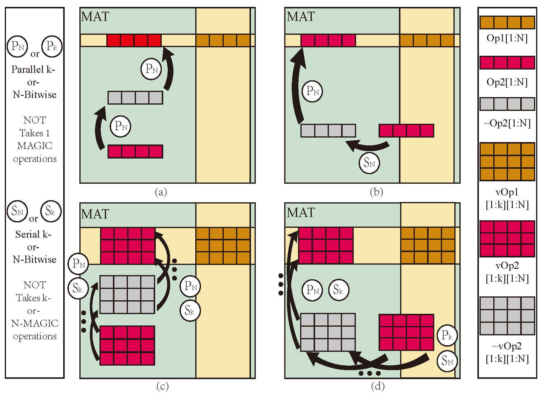
31]. In 2018, Talati et al. further discussed data transfer and parallelism based on a memristor MPU [
32], as shown in
Figure 1. However, this work uses memristor-aided logic (MAGIC) NOT as the basic logical operation, and data transmission to the destination position requires at least two steps of NOT operation, which seriously affects the operational efficiency of PiM.
The logic operation based on the memristor is the basis of realizing memristor PiM technology. Regarding the effective memristor logic design, the design of Sun et al. [
33] has realized the most efficient design of all logic gates, with the least number of devices and the least operation steps. The memristor logic operation can be divided into two categories. One is the logic operation structure based on a hybrid memristor–CMOS, such as the memristor adder circuit [
34] and the memristor multiplier circuit [
35]. These circuits use the nonvolatile nature of memristors to achieve faster particular logic operations but lack versatility. The second type is the logic operation based on memristor crossbar array, which has become the prominent architecture of PiM due to its good versatility. Realizing efficient logic operation in an array structure is the core problem of PiM design.
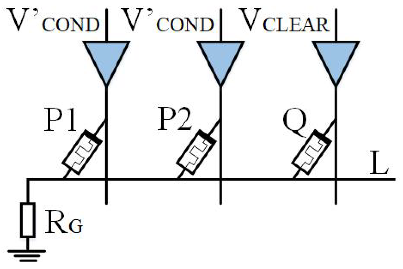
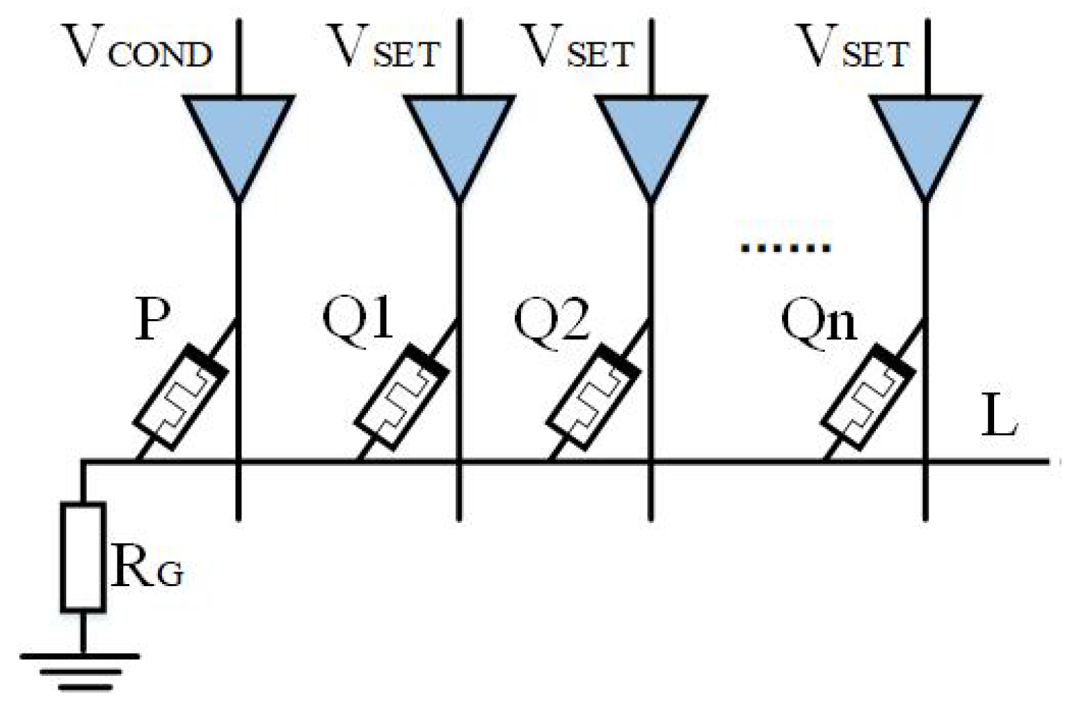
Material implication (IMPLY) [
36] is built based on a crossbar array structure. It is simple, reliable, and can implement complete Boolean logic operations, but its efficiency is relatively low. Kvatinsky et al. proposed MAGIC logic [
37], which separates operand and result and can implement logic gates such as IMP, XNOR, NAND, and OR. Jiang et al. proposed an MIMO logic gate based on IMPLY [
38], which can derive multiple new efficient logic operation methods and complete complex logic with fewer steps and memristors.
The computing system includes many fundamental logic blocks. The full adder (FA) is one of the most frequently used blocks. FA implementations include serial and parallel full adders. The serial FA requires fewer memristors but has multiple operating steps and low efficiency [
39]. On the other hand, the parallel FA requires fewer execution steps but involves more memristors in the calculation [
40]. A semiparallel FA has been proposed as a solution to achieve balance [
41]. In 2023, Jiang et al. proposed alternating crossbar array parallel FA based on MIMO logic, and alternating crossbar array achieves faster execution speed and fewer memristors [
38].
Multiplier is another complex logic operation module used in convolution, digital filtering, and fast Fourier transform (FFT) applications [
42]. It has significant complex logical operations and generates long-chain combination blocks with cascaded carry addition. Improving basic computing efficiency and reducing the carry step are the keys to achieving a high-efficiency multiplier.
Multipliers based on memristor crossbar array structures can be divided into matrix and exact multi-bit multipliers. Matrix operation is designed for matrix computing needs, such as convolution and image processing. This type of multiplier has high execution efficiency and good universality, but the calculation results are not accurate enough due to the analog signal operation mode [
43]. Unlike matrix multiplication, multi-bit multiplication is mainly aimed at computer logic operations and must provide accurate calculation results. Therefore, research on multi-bit multipliers starts with cell logic gates such as IMPLY and MAGIC and gradually completes the entire operation. For instance, Saeed et al. developed a binary multiplier that utilized the resistive characteristic of a memristor [
44]. Guckert et al. proposed a Dadda memristor multiplier; each cell contains two memristors and can achieve IMPLY operation in one cell [
45]. Furthermore, Mehri et al. proposed a special memristor–CMOS multiplier [
46]. However, the structure requires more CMOS switches and increased chip area. Yu et al. proposed a current-mode multi-memristor crossbar cell multiplier that effectively reduces power consumption. However, the calculation process is intricate [
47]. Radakovits et al. proposed a multiplier using semi-serial FA [
48], which has the least memristors and switches, but the execute steps are still high. Constructing a highly efficient multiplier with fewer devices and lower power consumption remains challenging.
This paper focuses on PiM MAT data transfer and logic operation efficiency and proposes a high-efficiency data transfer method and multiplier logic operation structure based on a memristor alternating crossbar array. The main works are as follows:
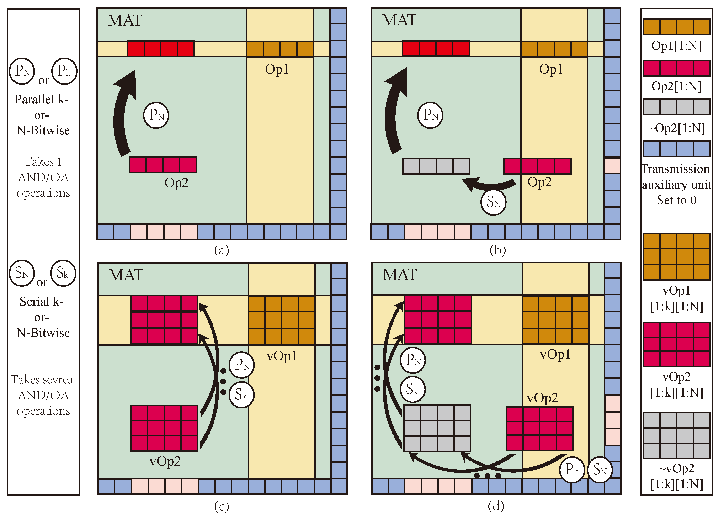
Improved data transfer efficiency in PiM MPU by reserving a row and column at the edge of the array for logic assistant based on AND and OA logic.
A multi-bit multiplier with fewer execution steps and devices and lower latency and power consumption is designed based on alternating crossbar array architecture and MIMO logic operations.
The paper is structured as follows: In
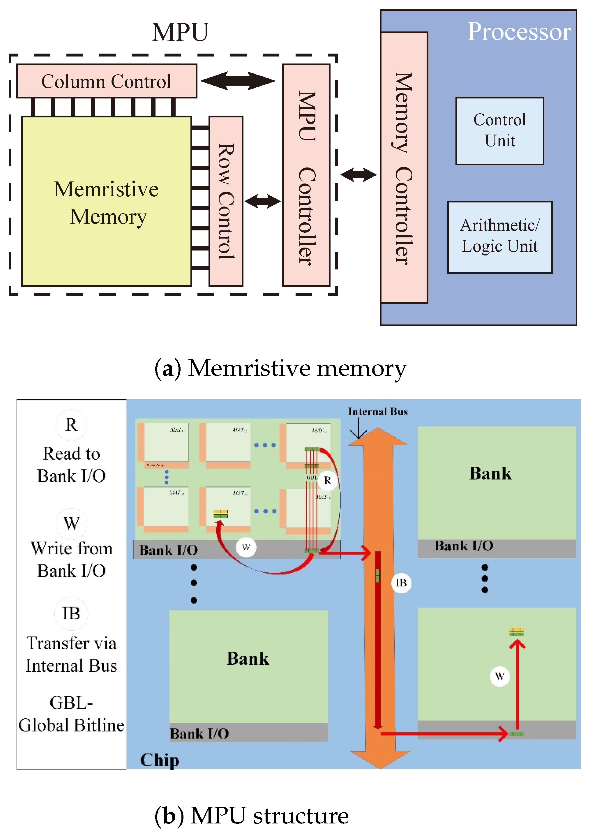
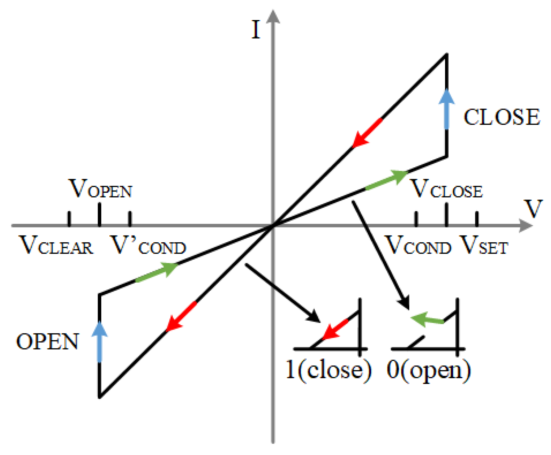
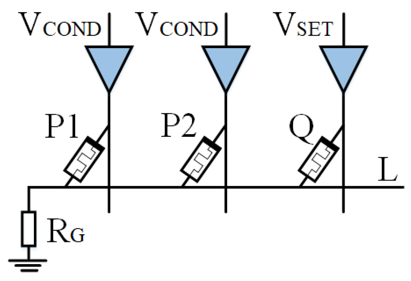
Section 2, we introduce the memristor model, MIMO memristive logic, PiM structure, and the multiplier’s working mechanism.
Section 3 describes the proposed data transfer within the MAT and the multiplier design method. In
Section 4, we showcase the correctness of our design through PSpice simulation. In addition,
Section 5 presents a comparison between different multipliers. Finally, in
Section 6, we conclude the paper.
4. Mul-Bit Multiplier Design
4.1. Multiplier Principle
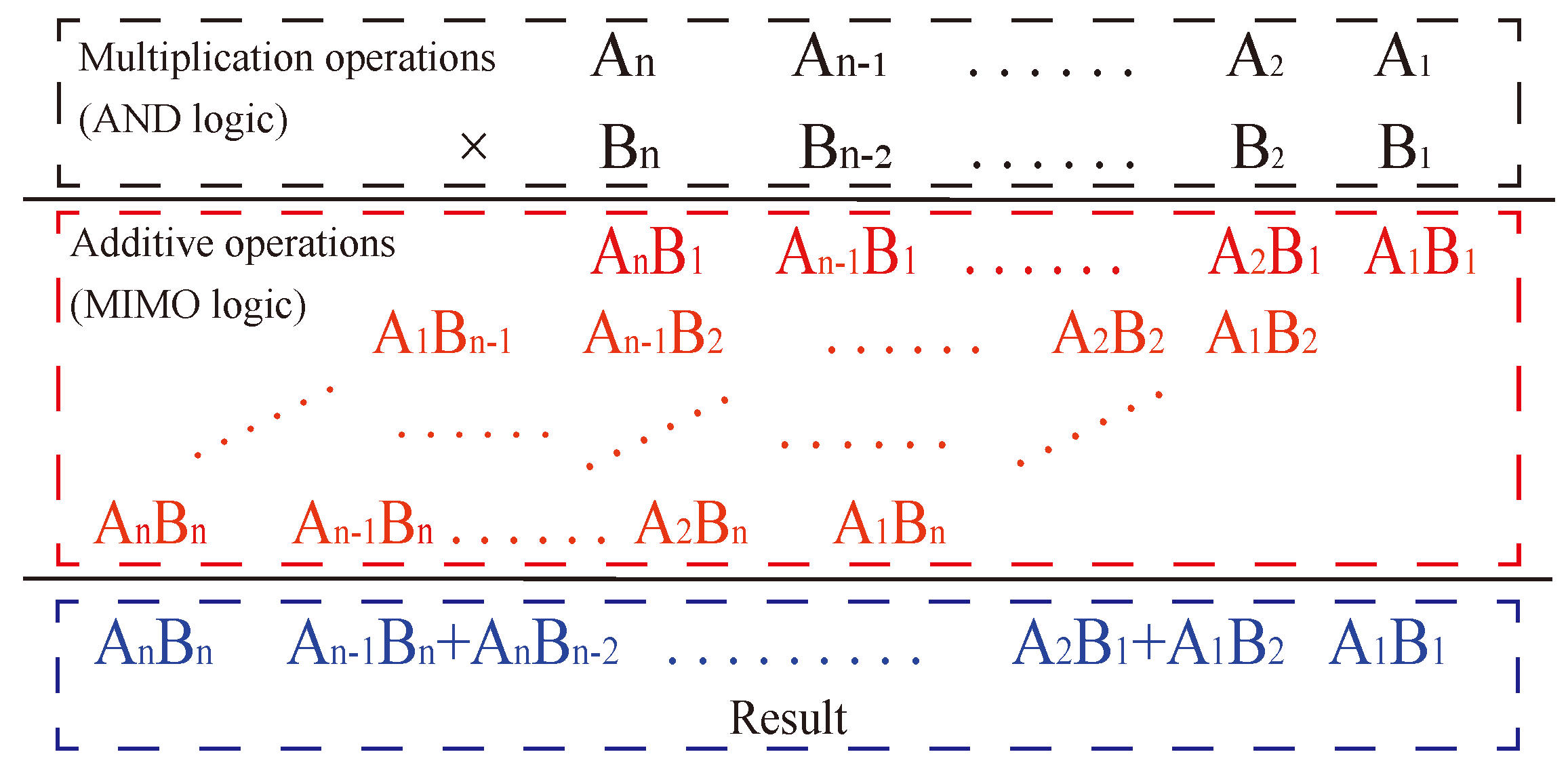
The multiplication formula consists of two parts, as shown in
Figure 11, starting with the multiplication operation of multiplying two one-digit numbers, also known as AND logic, followed by the summation of the corresponding position value, also known as an addition. Together, the two constitute the multiplication operation. Therefore, a multiplier can be realized by converting multiplication to addition with multiple digits.
The multiplier consists of multiple full adders and uses a crossbar array structure to convert the multiplication operation into a parallel operation of multiple full adders, which simplifies the operation while optimizing the number of MOS tubes in the circuit, improving the integration of the integrated circuit and making the circuit denser.
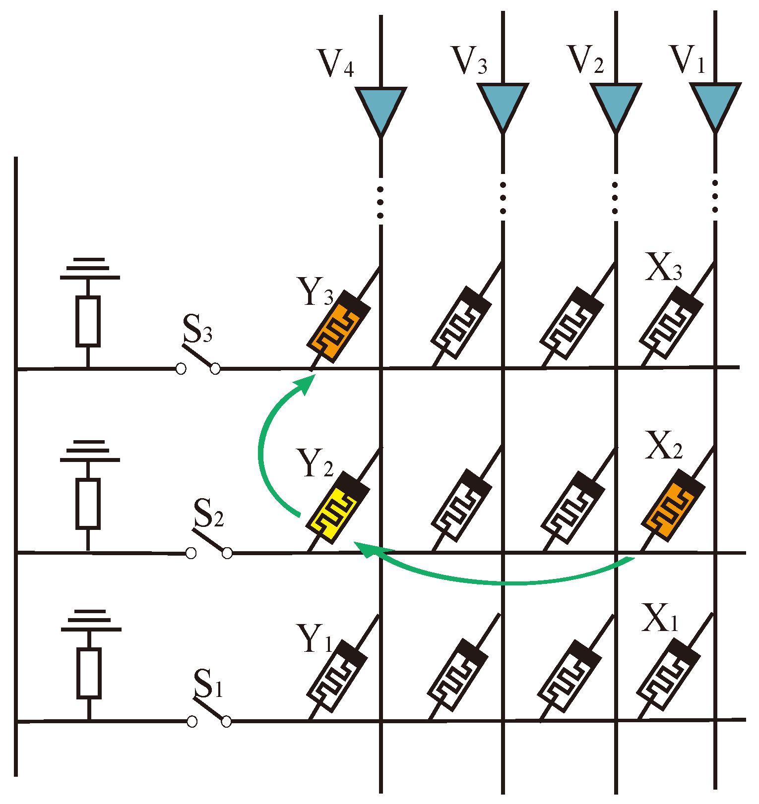
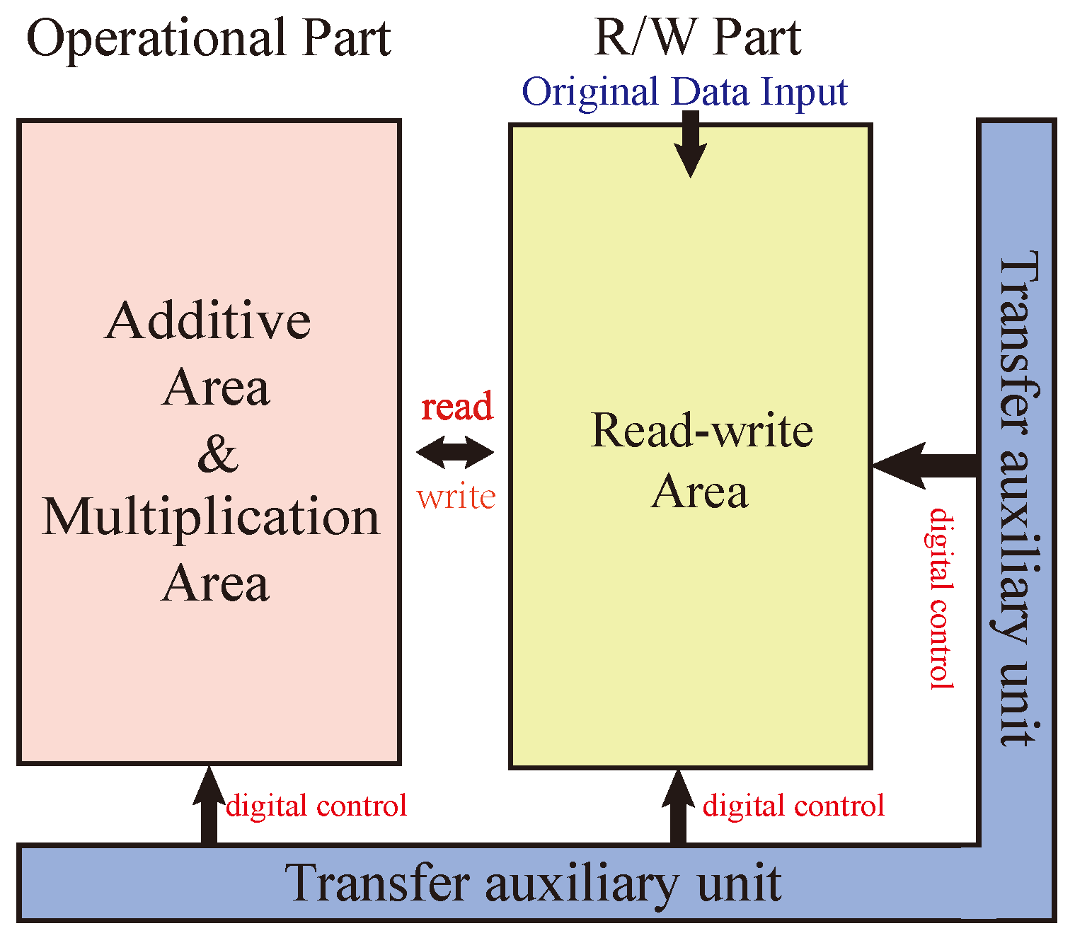
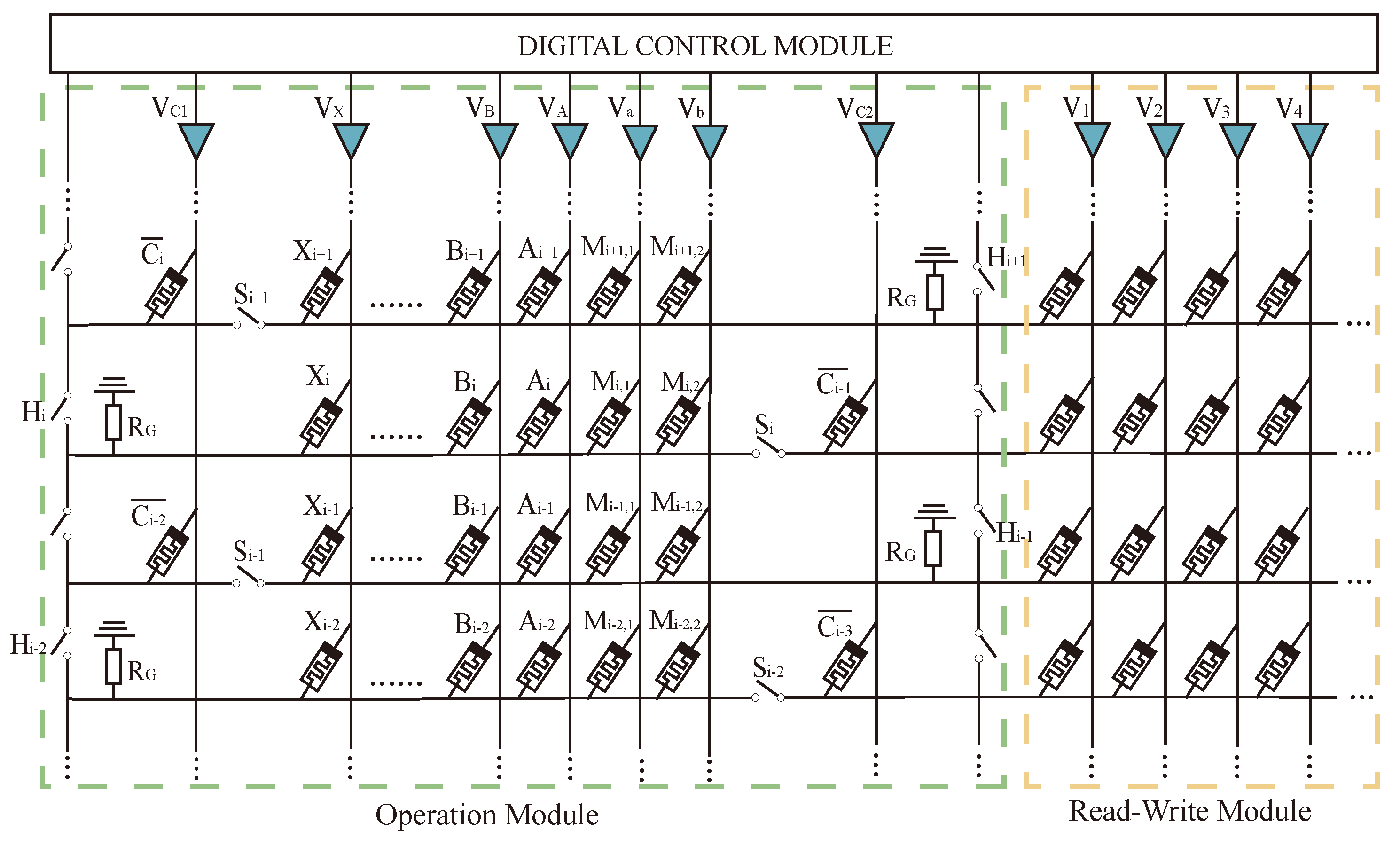
The whole multiplier circuit is divided into three parts: one for arithmetic, one for storage, and one for data transfer auxiliary cells. The structure of the Operational Part adopts the alternating crossbar array structure mentioned previously. In each row, there are several memristors,
,
, …,
, and
, responsible for performing the arithmetic. The memristor
is responsible for holding the rounding function; the two types of memristors are separated by switches,
. Between the rows, there are cross-arranged switches,
, for the control of the steps of the operations. The Operational Part is required to perform both multiplication and addition calculations. The read/write section (R/W Part) is responsible for writing and reading data, and this section can write and save the data from being calculated or the data output from the Operational Part, or it can read the data from this section and input it to the Operational Part for calculation. The data transmission auxiliary unit is a series of memristors located at the right and bottom of the array and is used to assist the transfer of data, which is usually set to logic 0 to facilitate the execution of OA logic. All these three sections form the multiplier’s arithmetic circuit, as shown in
Figure 12.
4.2. Multiplier Operations
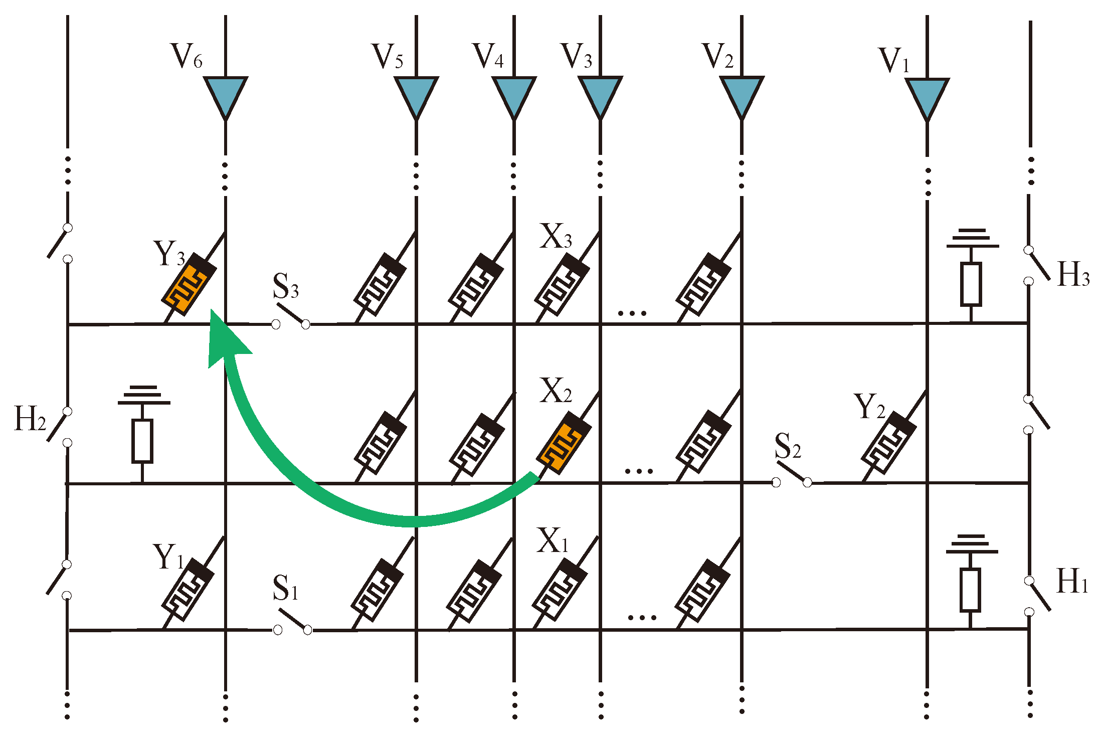
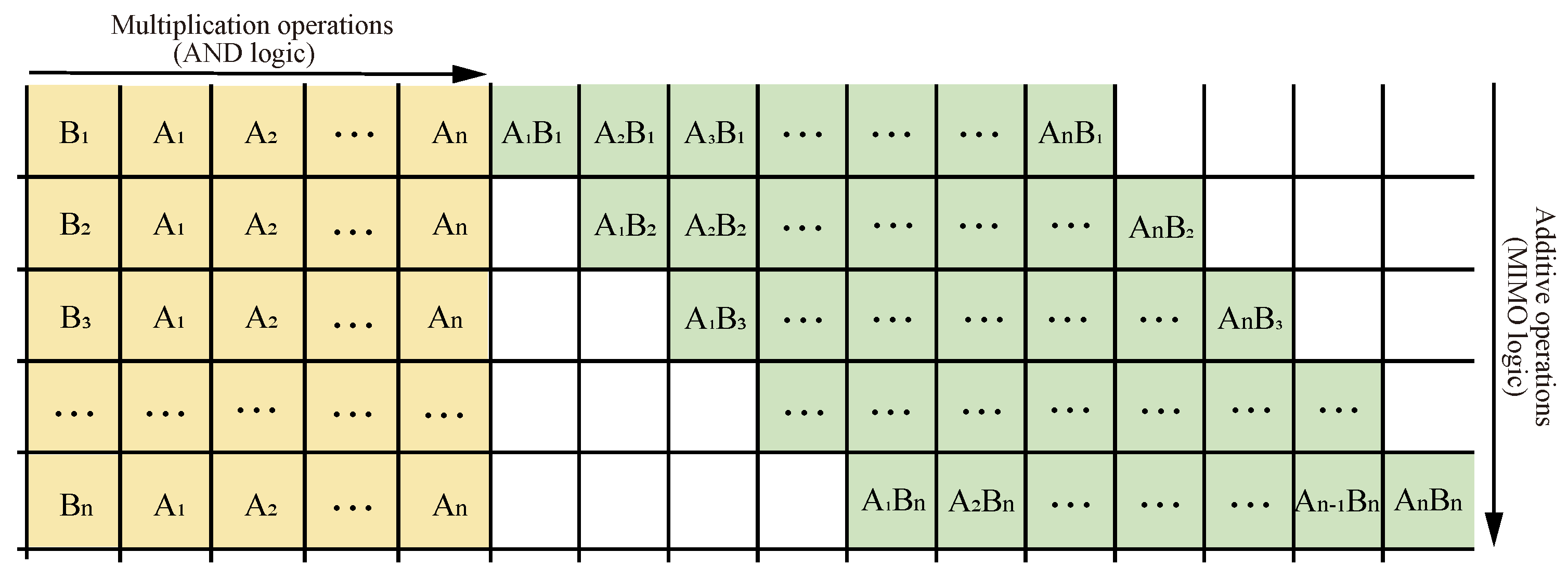
Take a multiplier as an example; the multipliers are , and , . The operation steps of this multiplier are as follows:
Step 1: Read and input the data from the read/write area into the multiplication area of the operational part through the designed transmission method. The layout of the multiplication area is shown in the yellow part in
Figure 13. For a
multiplier,
stores in memristor
,
stores in memristor
,
stores in memristor
and
, and
stores in memristor
and
, as shown in
Figure 14.
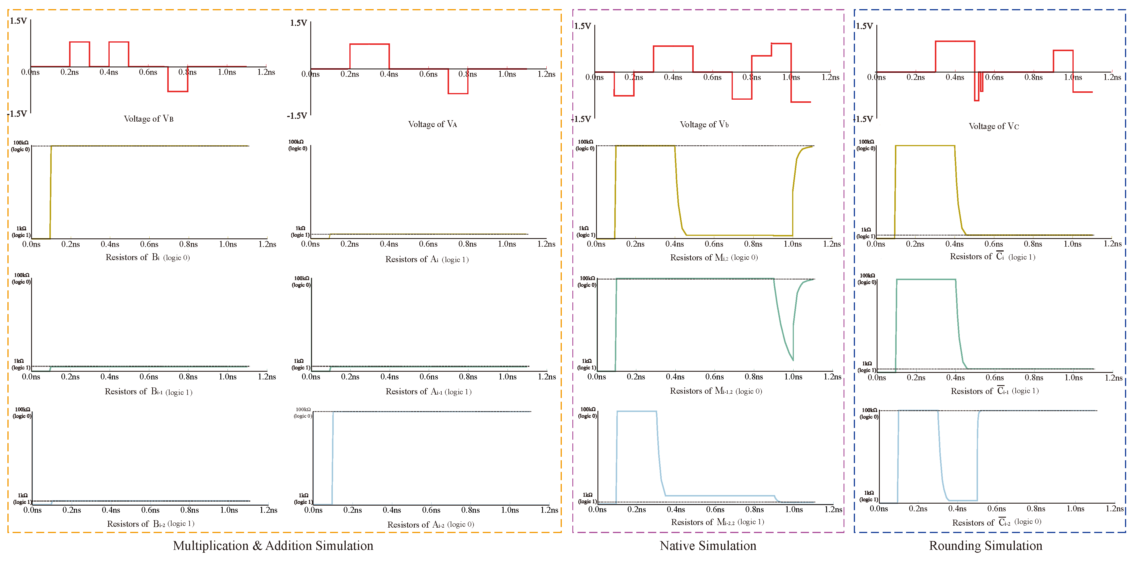
Step 2: Perform the multiplication operation. The logic of the operation is AND logic, and the truth table of the logic is shown in
Table 3; the multiplication obtains four results:
,
,
, and
. The result data will be directly input into the additive area. As shown in the green part in
Figure 13,
stores in memristor
,
stores in memristor
,
stores in memristor
, and
stores in memristor
. For a
multiplier, the addition area will be performed on three rows in the next few steps.
and 0 are added together,
and
are added together, and
and 0 are added together.
Steps 3 and 4: Turn on the switches , , and . Disconnect the switches on all columns. The full adder module can calculate step 3 and step 4 simultaneously. At this stage, the multiplier only needs two steps through parallel calculation.
Steps 5 and 6: Turn on the switches and , . Disconnect the switch , , , and all other switches. In this way, the memristor can be connected to , the memristor can be connected to , and the memristor can be connected to without affecting other bits, so data transmission can be realized between the carrier and the standard. As in steps 3 and 4, the multiplier can also complete steps 5 and 6 in parallel. At this stage, parallel computing requires two steps.
Step 7: Turn on the switches , , and , , . Disconnect all other switches. By preparing steps 3 to 6 and applying an alternating crossbar array, we can complete the current bit’s carry calculation in one step.
Step 8 to Step 12: Turn on the switch
,
,
. Disconnect the switches on all columns. After completing step 7,
,
,
receive the carry from the adjacent lower bits, and each bit can independently complete all the remaining steps. Therefore, the full adder module can complete the next steps in parallel. At this stage, the parallel calculation of the multiplier takes five steps. All the operation steps are shown in
Table 4. There are a total of 12 steps in a
multiplication operation.
Next, we can extend the multiplier to an multiplier with the same steps as the multiplier; the first four steps are the same as those of the multiplier, while in the steps of the addition algorithm, for multi-bit addition, we need to add every two values of the additive number and store the intermediate value into the read–write region. Thus, the steps of the addition algorithm are (n − 1)(n + 9). The bit multiplier requires total steps steps.
6. Conclusions
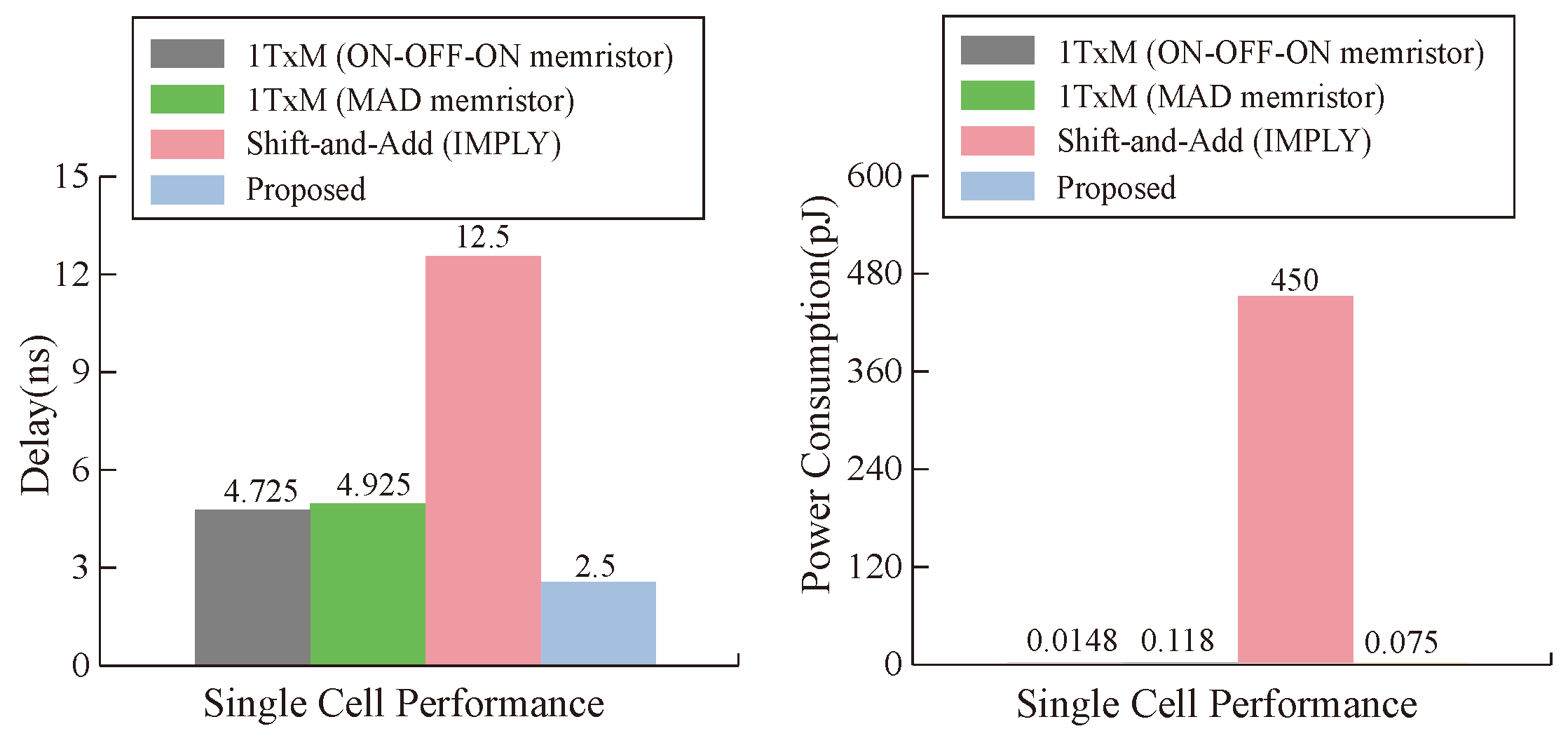
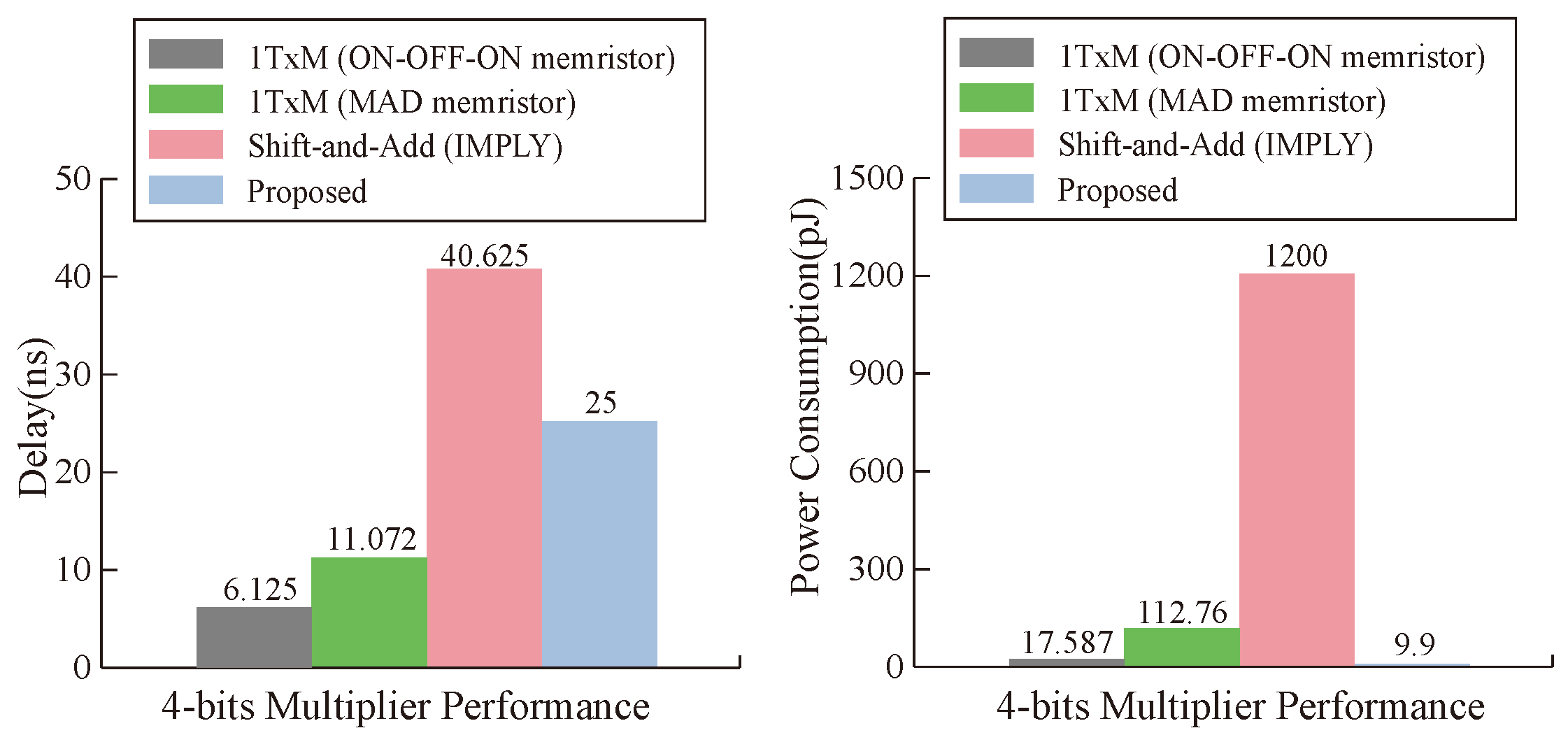
This paper proposes an efficient PiM MAT data transmission method based on the alternating crossbar array and further proposes a multi-bit multiplier design scheme. The proposed data transmission method reserves the row and column edges as temporary assistant cells, employs OA logic as the moving logic, significantly reduces data transmission steps, and improves efficiency. The proposed multi-bit multiplier converts multiplication operations to multi-bit addition operations, greatly improving multiplier execution efficiency. Compared to existing memristive multipliers, it has lower latency and power consumption, higher reliability, and greater flexibility. This work is of great significance for promoting research on high-performance PiM.
Our model is based on the ideal memristor, and the control voltage needs to be adjusted according to the actual memristor characteristics when it is implemented. In addition, the problem of leakage current is not discussed in this paper. In the following research, it is necessary to comprehensively evaluate the characteristics of power consumption, delay, storage density, and so on, according to the specific implementation process to provide guidance for circuit design.
As the number of calculation bits increases, the proposed multiplier’s latency gradually increases, which is not conducive to its fast and efficient operation. In the future, we will simplify the multiplier’s operation steps to gradually improve the problem of excessive time extension.


