


Design and Fabrication of Continuous Surface Optical Field Modulator for Angular Spectrum Discreteness Compensation

Abstract
:1. Introduction
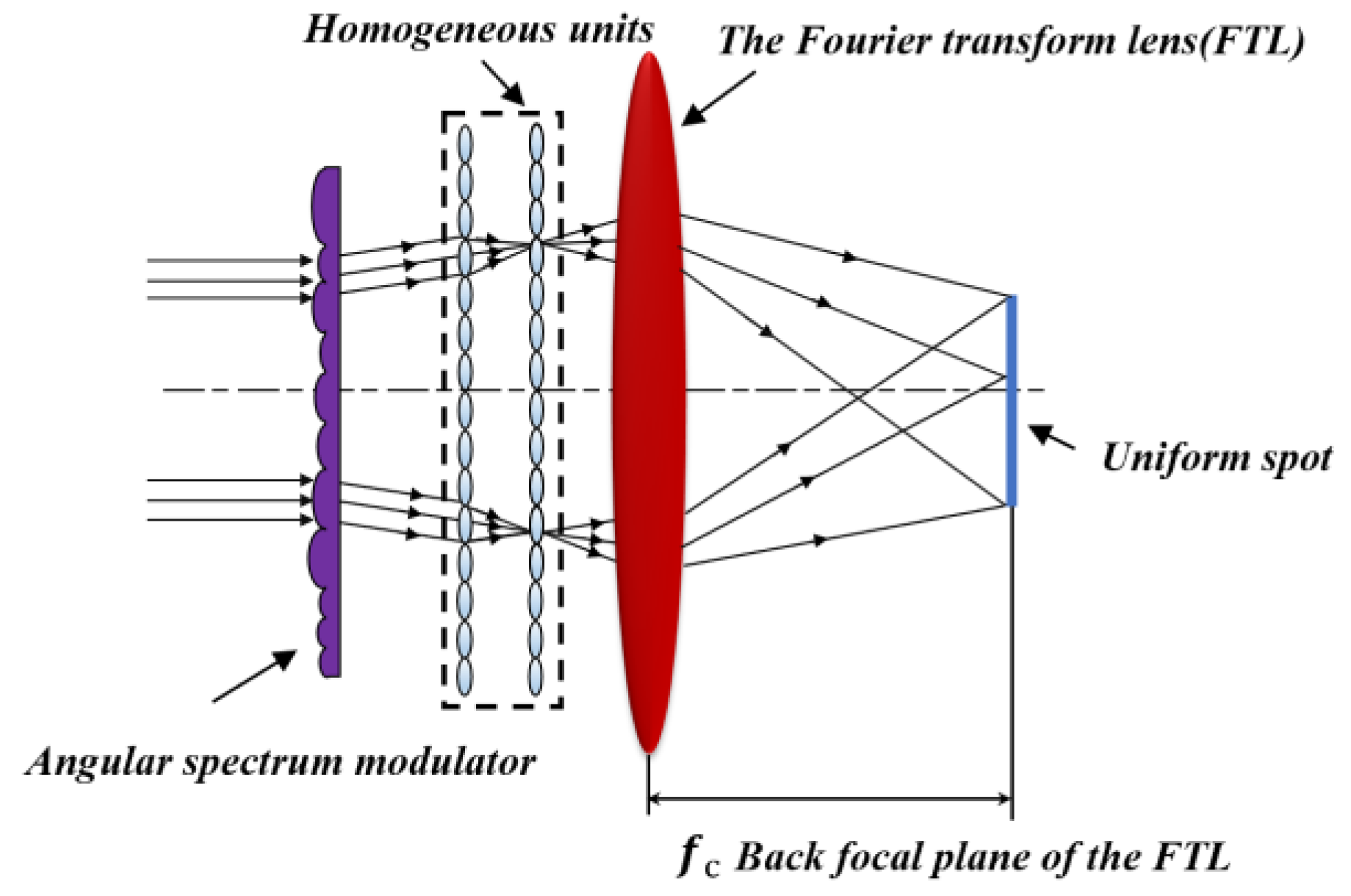
2. Theory
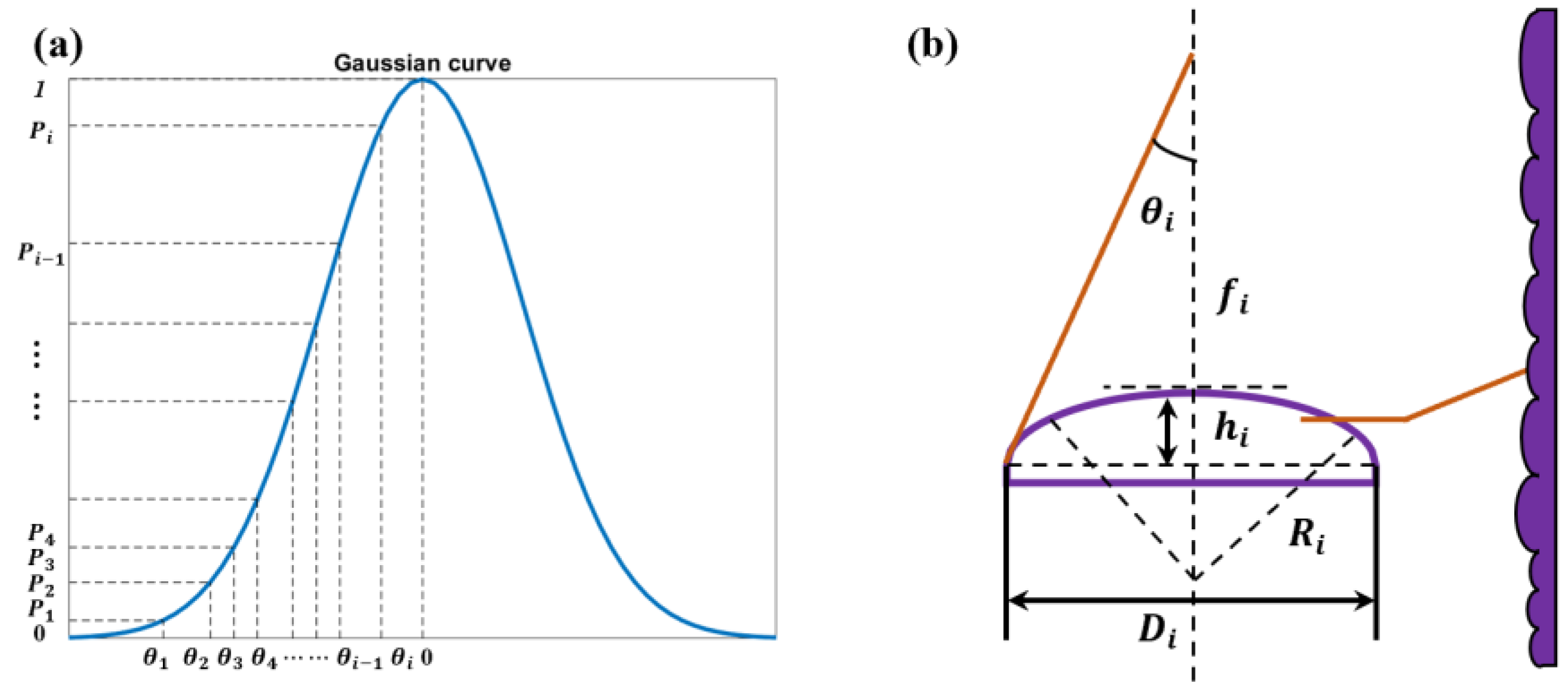
2.1. Principles of Structural Parameter Design
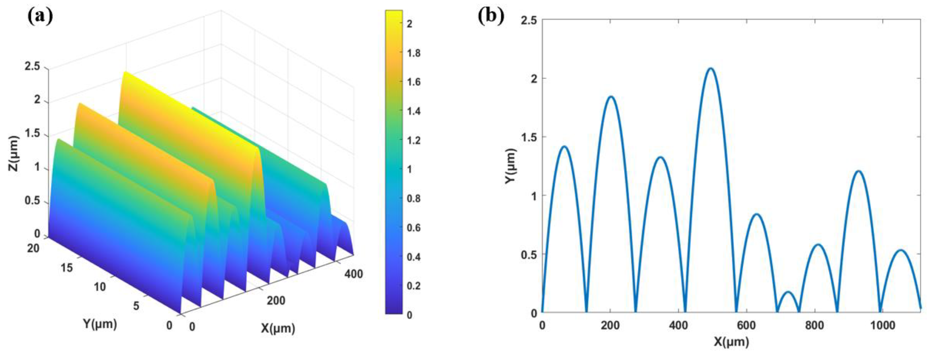
2.2. Numerical Simulation of Scattered Optical Field
3. Design and Simulation
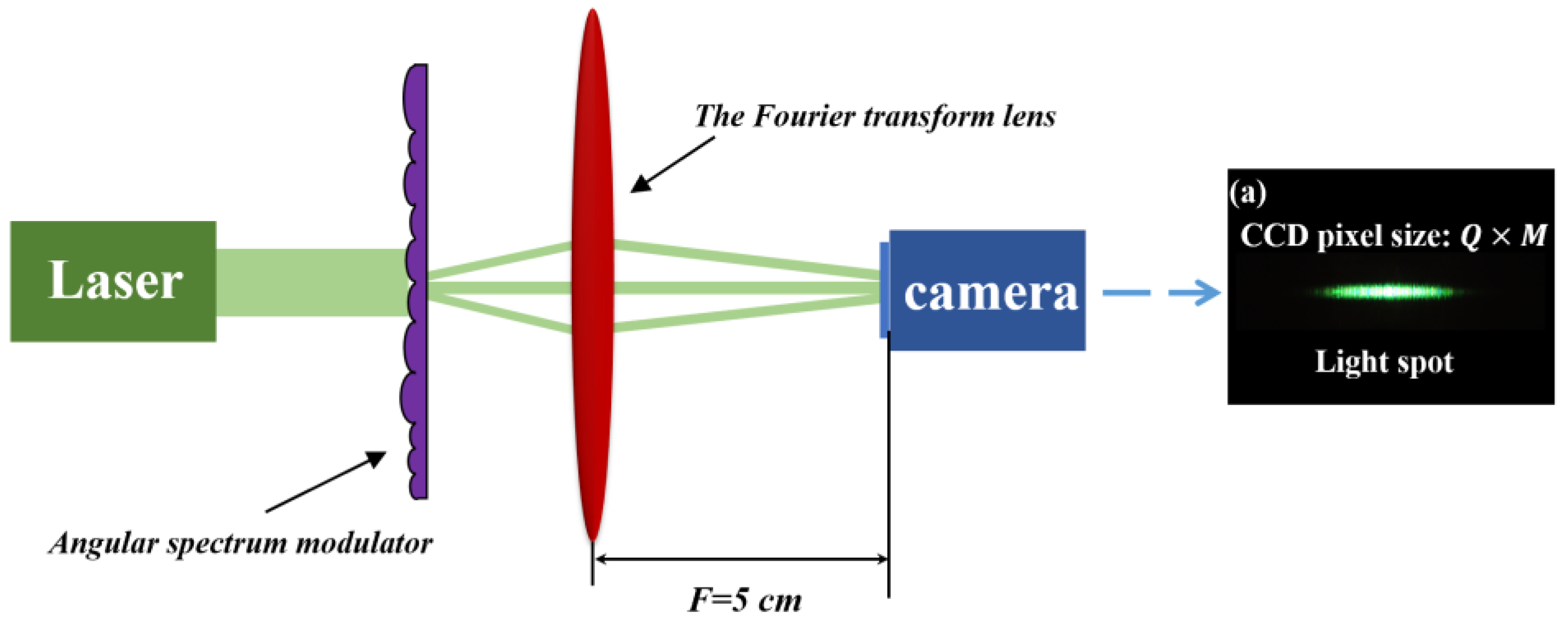
4. Experiments and Discussion
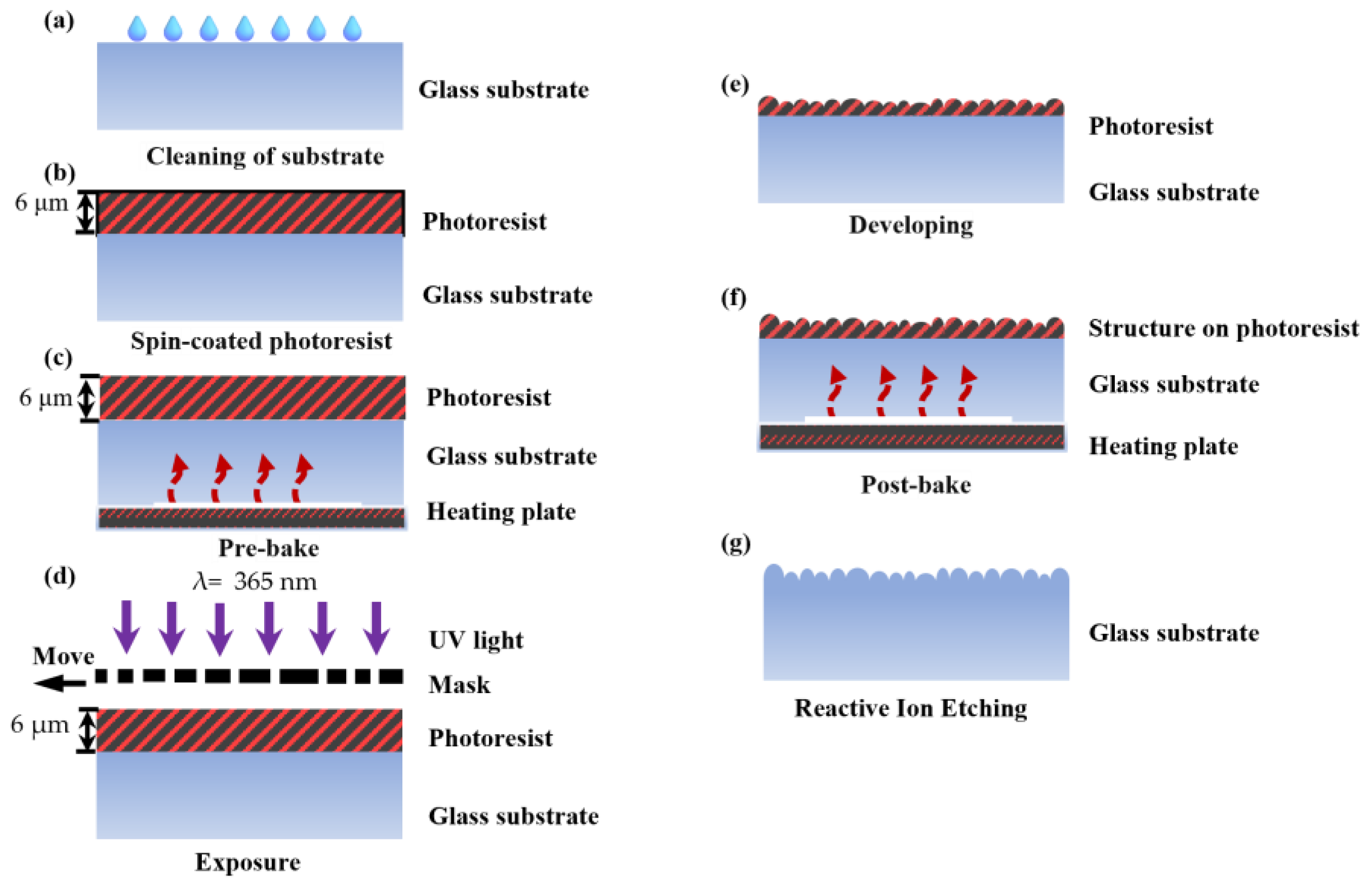
4.1. Manufacturing Procedure
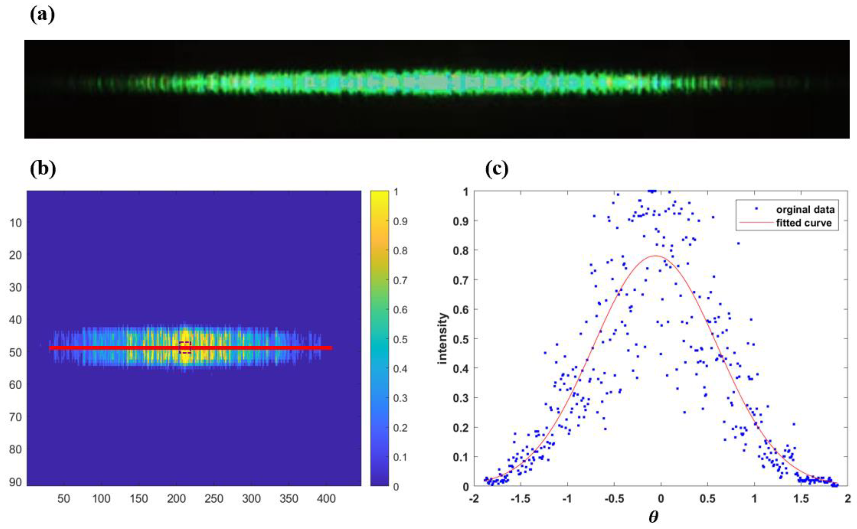
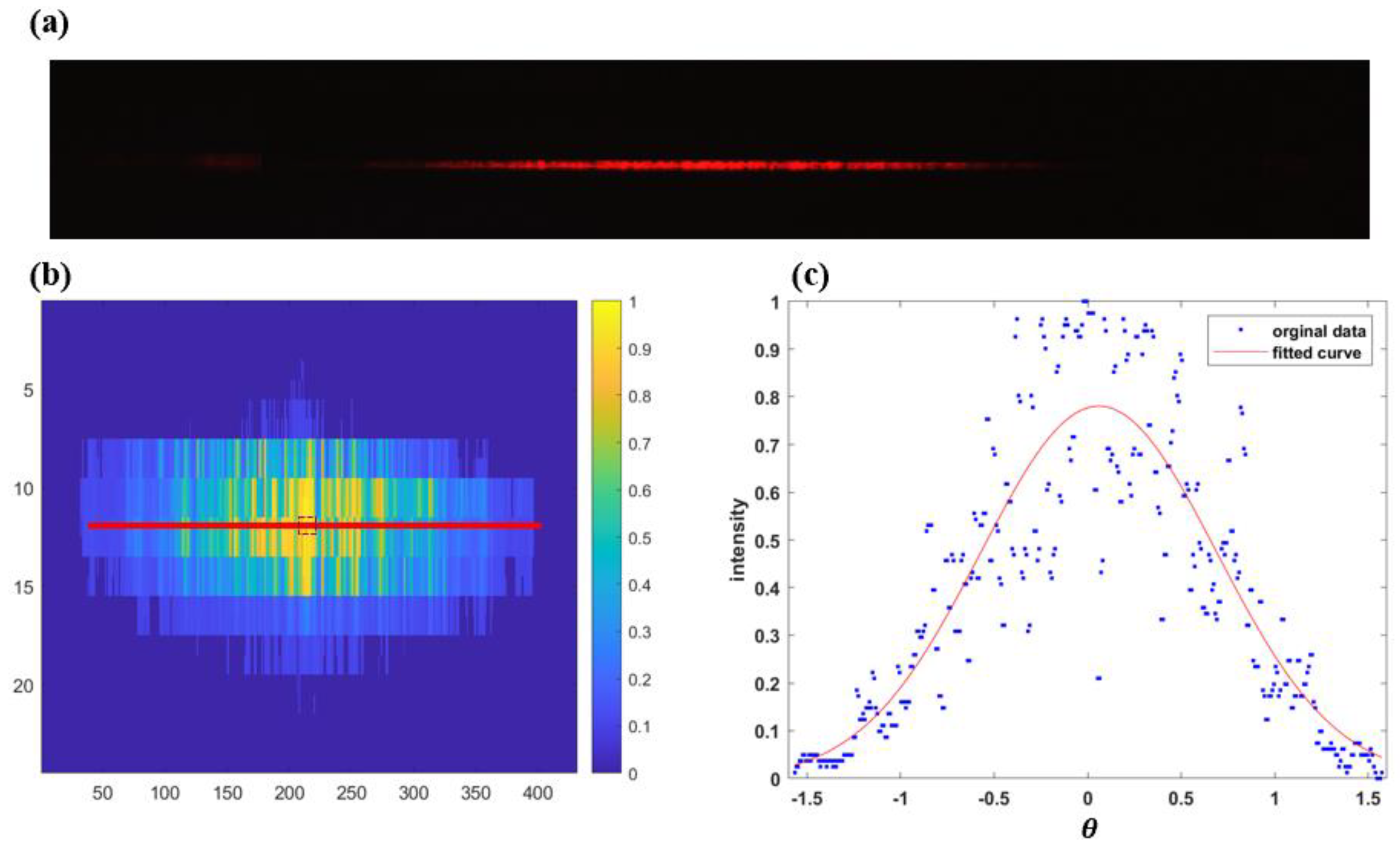
4.2. Measurement and Characterization
4.3. Optical Experiments and Discussion
5. Conclusions
Author Contributions
Funding
Data Availability Statement
Conflicts of Interest
References
- Leu, M.Y.; Whang, A.J.W.; Chen, Y.Y. A novel design freeform reflector application applied to natural light illumination system. In Proceedings of the International Optical Design Conference, Online, 27 June–1 July 2021; Optica Publishing Group: Washington, DC, USA, 2021; p. 120781L. [Google Scholar]
- Gao, S.; Tsyganok, E.A.; Romanova, G.E. Comparative research of mirror systems for extreme ultraviolet lithography illuminator. In Proceedings of the Optical Design and Testing XIII, Beijing, China, 14–15 October 2023; SPIE: Bellingham, WA, USA, 2023; Volume 12765, pp. 68–71. [Google Scholar]
- Liu, J.; Hu, S.; Li, Q. Compact ultraviolet light-emitting diode-based lithography illumination system with tunable coherent factor. Opt. Eng. 2023, 62, 045103. [Google Scholar] [CrossRef]
- Bai, X.; Jing, X.; Liao, N. Design method for the high optical efficiency and uniformity illumination system of the projector. Opt. Express 2021, 29, 12502–12515. [Google Scholar] [CrossRef] [PubMed]
- He, Y.; Xing, T.W.; Lin, W.M.; Liao, Z.J.; Liu, W.J. Method for illumination uniformity correction in the illumination system of lithography. Optik 2021, 228, 166172. [Google Scholar] [CrossRef]
- Herkommer, A.M. Evolution of Illumination Systems in Microlithography A Retrospective. In Proceedings of the International Optical Design Conference, Jackson Hole, WY, USA, 13–17 June 2010; Optica Publishing Group: Washington, DC, USA, 2010; p. ITuC1. [Google Scholar]
- Gong, J.; Zhou, J.; Liu, J.; Hu, S.; Wang, J.; Sun, H. Mask-Moving-Lithography-Based High-Precision Surface Fabrication Method for Microlens Arrays. Micromachines 2024, 15, 289. [Google Scholar] [CrossRef] [PubMed]
- Cao, A.; Pang, H.; Wang, J.; Zhang, M.; Shi, L.; Deng, Q. Center off-axis tandem microlens arrays for beam homogenization. IEEE Photonics J. 2015, 7, 2400207. [Google Scholar] [CrossRef]
- Ganser, H.; Darscht, M.; Miklyaev, Y. High-throughput homogenizers for hyper-NA illumination systems. In Proceedings of the Optical Microlithography XIX, San Jose, CA, USA, 21–24 February 2006; SPIE: Bellingham, WA, USA, 2006; Volume 6154, pp. 881–891. [Google Scholar]
- Li, Y. Analysis of factors affecting homogenization effect of homogenizing rod in laser lighting system. In Proceedings of the 2020 International Conference on Optoelectronic Materials and Devices, Guangzhou, China, 18–20 December 2021; SPIE: Bellingham, WA, USA, 2021; Volume 11767, p. 1176702. [Google Scholar]
- Rausch, D.; Herkommer, A.M. Phase space approach to the use of integrator rods and optical arrays in illumination systems. Adv. Opt. Technol. 2012, 1, 69–78. [Google Scholar] [CrossRef]
- Iwasaki, K.; Hayashi, T.; Goto, T. Square and uniform laser output device: Theory and applications. Appl. Opt. 1990, 29, 1736–1744. [Google Scholar] [CrossRef] [PubMed]
- Mei, Q.; Li, Y. Design of three-mirror illumination system with free-form fly’s eye for extreme ultraviolet lithography. Appl. Opt. 2015, 54, 2091–2097. [Google Scholar] [CrossRef] [PubMed]
- Urey, H.; Powell, K.D. Microlens-array-based exit-pupil expander for full-color displays. Appl. Opt. 2005, 44, 4930–4936. [Google Scholar] [CrossRef]
- Levinson, H.J. Principles of Lithography; SPIE Press: Bellingham, WA, USA, 2005; Volume 146. [Google Scholar]
- Chen, M.; Wang, Y.; Zeng, A.; Zhu, J.; Yang, B.; Huang, H. Flat Gauss illumination for the step-and-scan lithographic system. Opt. Commun. 2016, 372, 201–209. [Google Scholar] [CrossRef]
- Chen, M.; Chen, L.; Zeng, A.; Zhu, J.; Yang, B.; Huang, H. Generation of trapezoidal illumination for the step-and-scan lithographic system. Appl. Opt. 2015, 54, 6820–6826. [Google Scholar] [CrossRef] [PubMed]
- Fiolka, D. Illumination System for a Microlithographic Projection Exposure Apparatus. U.S. Patent Application 11/191,925, 2006. [Google Scholar]
- Deng, Z.; Yang, Q.; Chen, F. High-performance laser beam homogenizer based on double-sided concave microlens. IEEE Photonics Technol. Lett. 2014, 26, 2086–2089. [Google Scholar] [CrossRef]
- Bitterli, R.; Scharf, T.; Herzig, H.P. Fabrication and characterization of linear diffusers based on concave micro lens arrays. Opt. Express 2010, 18, 14251–14261. [Google Scholar] [CrossRef] [PubMed]
- Ma, X.; Zhang, F.; Niu, Z. Design and optimization of top-Gaussian illumination field in photolithography. Opt. Eng. 2021, 60, 025106. [Google Scholar] [CrossRef]
- Rui, D.; Yang, H. A telecentricity matching design for non-critical lithography: Incorporating homogenization induced discreteness of pupil pattern. Opt. Commun. 2020, 476, 126314. [Google Scholar] [CrossRef]
- Wang, J.; Zhao, Y.; Zhang, B. Optical design of athermalized infrared dual-band annular folded lens with multilayer imaging diffractive optical elements. Opt. Lasers Eng. 2023, 161, 107370. [Google Scholar] [CrossRef]
- Xu, N.; Xu, H.; Chen, S.; Hu, H.; Xu, Z.; Feng, H. Snapshot hyperspectral imaging based on equalization designed DOE. Opt. Express 2023, 31, 20489–20504. [Google Scholar] [CrossRef] [PubMed]
- Liang, C.; Zhang, W.; Rui, D. High-performance laser projection display illumination system based on a diffractive optical element. Appl. Opt. 2017, 56, 2810–2815. [Google Scholar] [CrossRef] [PubMed]
- Du, J.; Li, F.; Peng, F. Large-range and high-precision autofocus method based on an annular DOE for a laser direct writing system. Opt. Express 2022, 30, 6981–6990. [Google Scholar] [CrossRef]
- Liu, J.S.; Caley, A.J.; Waddie, A.J. Comparison of simulated quenching algorithms for design of diffractive optical elements. Appl. Opt. 2008, 47, 807–816. [Google Scholar] [CrossRef]
- Zhou, W.; Li, R.; Li, M. Fabrication of microlens array on chalcogenide glass by wet etching-assisted femtosecond laser direct writing. Ceram. Int. 2022, 48, 18983–18988. [Google Scholar] [CrossRef]
- Hwang, S.; Kim, T.; Lee, J. Design of square-shaped beam homogenizer for petawatt-class Ti: Sapphire amplifier. Opt. Express 2017, 25, 9511–9520. [Google Scholar] [CrossRef]
- Xue, L.; Pang, Y.; Liu, W. Fabrication of random microlens array for laser beam homogenization with high efficiency. Micromachines 2020, 11, 338. [Google Scholar] [CrossRef]
- Huang, P.; Dong, X.C.; He, C.W. Square-aperture microlens array fabrication by the moving mask technology. DEStech Trans. Eng. Technol. Res. 2017, 153–158. [Google Scholar] [CrossRef]
- Joseph, W. Introduction to Fourier Optics, 3rd ed.; Roberts and Company Publishers: Englewood, CO, USA, 2005. [Google Scholar]
- Yuan, W.; Cai, Y.; Xu, C. Fabrication of multifocal microlens array by one step exposure process. Micromachines 2021, 12, 1097. [Google Scholar] [CrossRef]


| 1 | 2 | 3 | 4 | 5 | 6 | 7 | 8 | 9 | |
|---|---|---|---|---|---|---|---|---|---|
| 0.08 | 0.12 | 0.22 | 0.30 | 0.34 | 0.53 | 0.71 | 0.78 | 0.91 | |
| 1.47 | 1.35 | 1.15 | 1.02 | 0.96 | 0.74 | 0.55 | 0.46 | 0.29 | |
| 149.5 | 144 | 130 | 125.4 | 145.6 | 120 | 112 | 121.6 | 64 | |
| 1341.1 | 1407 | 1491.3 | 1627.6 | 1998.9 | 2141.6 | 2700 | 3463.6 | 2900 | |
| 2083.2 | 1842 | 1416.5 | 1325.7 | 1325.7 | 840 | 580 | 533.6 | 176 |
| Lithography Process | Parameter |
|---|---|
| Cleaning of substrate | Chemical solution cleaning, drying |
| Spin-coated photoresist | 10XT, 4000 rpm/min, 40 s |
| Pre-bake | 100 °C, 5 min, 6 µm |
| Exposure | λ = 365 nm, 3.5 mW/cm2, pre-exposure 5 s |
| Developing | AZ400K:Deionized H2O = 2:3, 25 s |
| Post-bake | 110 °C, 30 min |
| Reactive ion etching | SF6:CHF3 = 23:33, t = 5000 s, P = 1.5 Pa |
Disclaimer/Publisher’s Note: The statements, opinions and data contained in all publications are solely those of the individual author(s) and contributor(s) and not of MDPI and/or the editor(s). MDPI and/or the editor(s) disclaim responsibility for any injury to people or property resulting from any ideas, methods, instructions or products referred to in the content. |
© 2024 by the authors. Licensee MDPI, Basel, Switzerland. This article is an open access article distributed under the terms and conditions of the Creative Commons Attribution (CC BY) license (https://creativecommons.org/licenses/by/4.0/).
Share and Cite
Xiao, M.; Cao, A.; Xu, C.; Pang, H.; Fu, Y.; Deng, Q. Design and Fabrication of Continuous Surface Optical Field Modulator for Angular Spectrum Discreteness Compensation. Micromachines 2024, 15, 952. https://doi.org/10.3390/mi15080952
Xiao M, Cao A, Xu C, Pang H, Fu Y, Deng Q. Design and Fabrication of Continuous Surface Optical Field Modulator for Angular Spectrum Discreteness Compensation. Micromachines. 2024; 15(8):952. https://doi.org/10.3390/mi15080952
Chicago/Turabian StyleXiao, Min, Axiu Cao, Cheng Xu, Hui Pang, Yongqi Fu, and Qiling Deng. 2024. "Design and Fabrication of Continuous Surface Optical Field Modulator for Angular Spectrum Discreteness Compensation" Micromachines 15, no. 8: 952. https://doi.org/10.3390/mi15080952