

A Sub-0.01 °C Resolution All-CMOS Temperature Sensor with 0.43 °C/−0.38 °C Inaccuracy and 1.9 pJ · K2 Resolution FoM for IoT Applications


Abstract
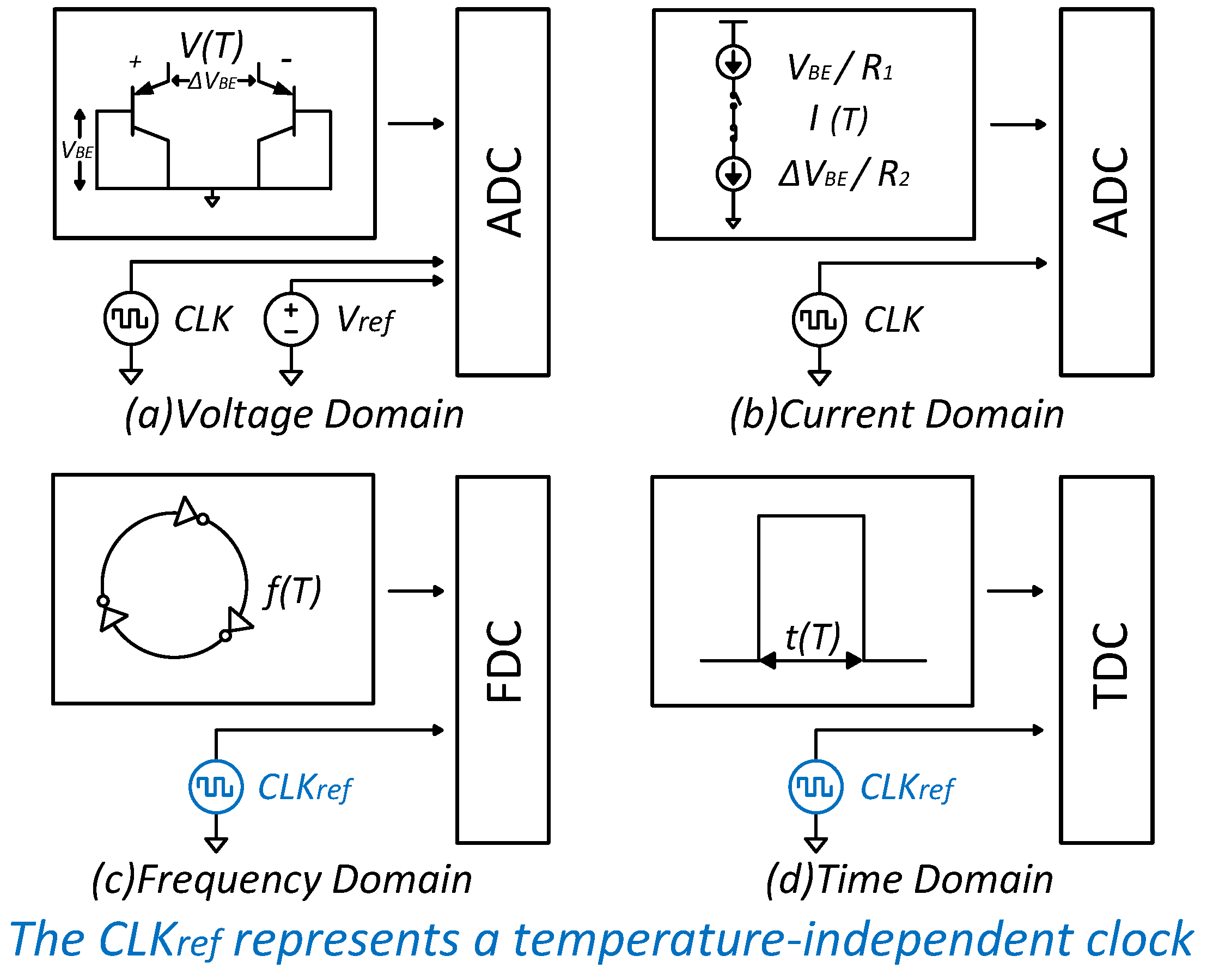
:1. Introduction
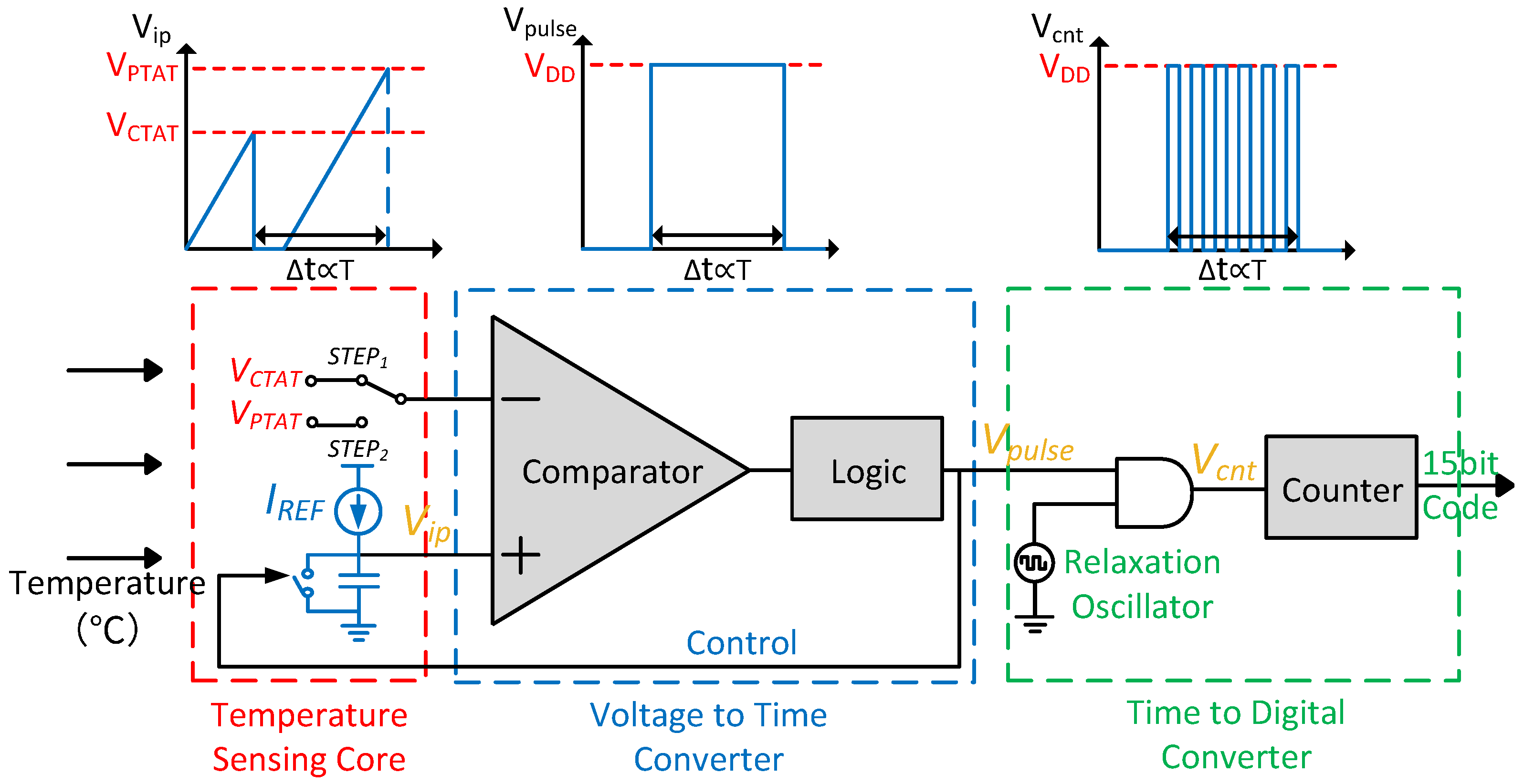
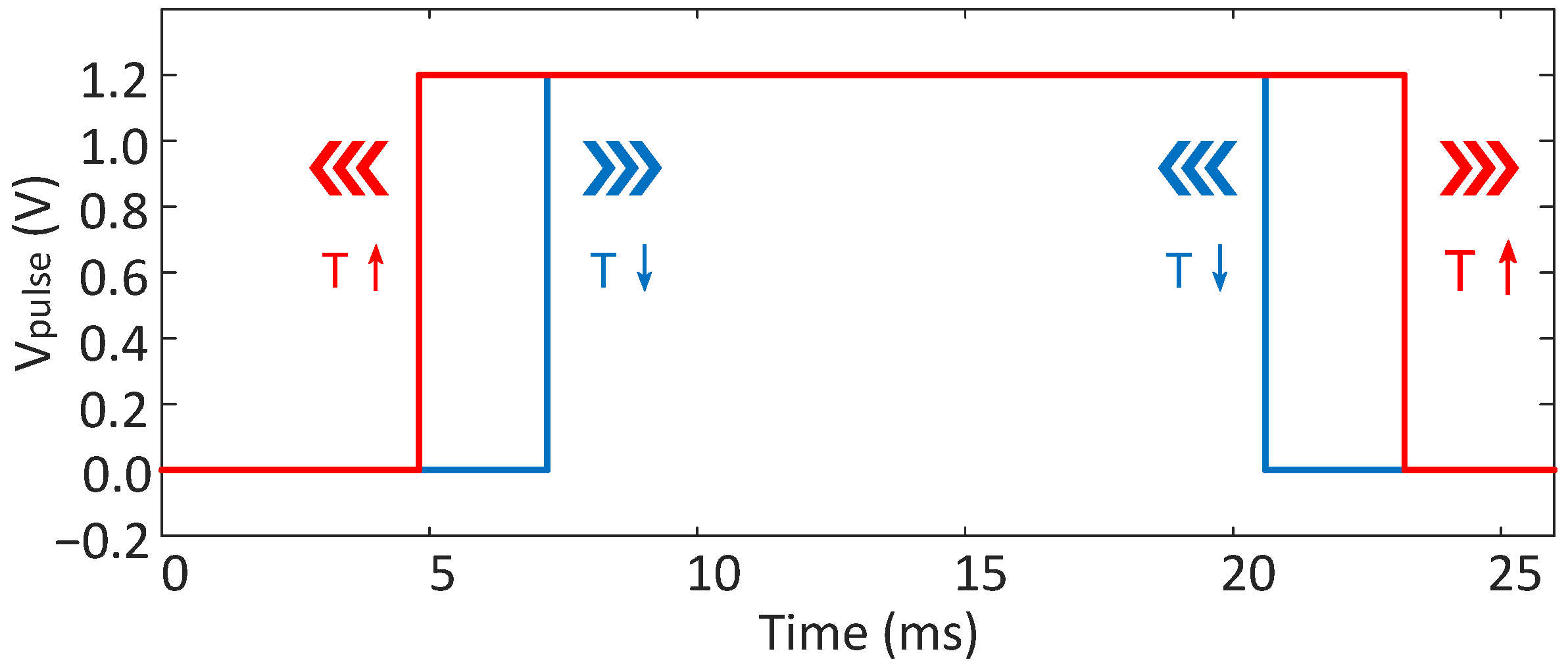
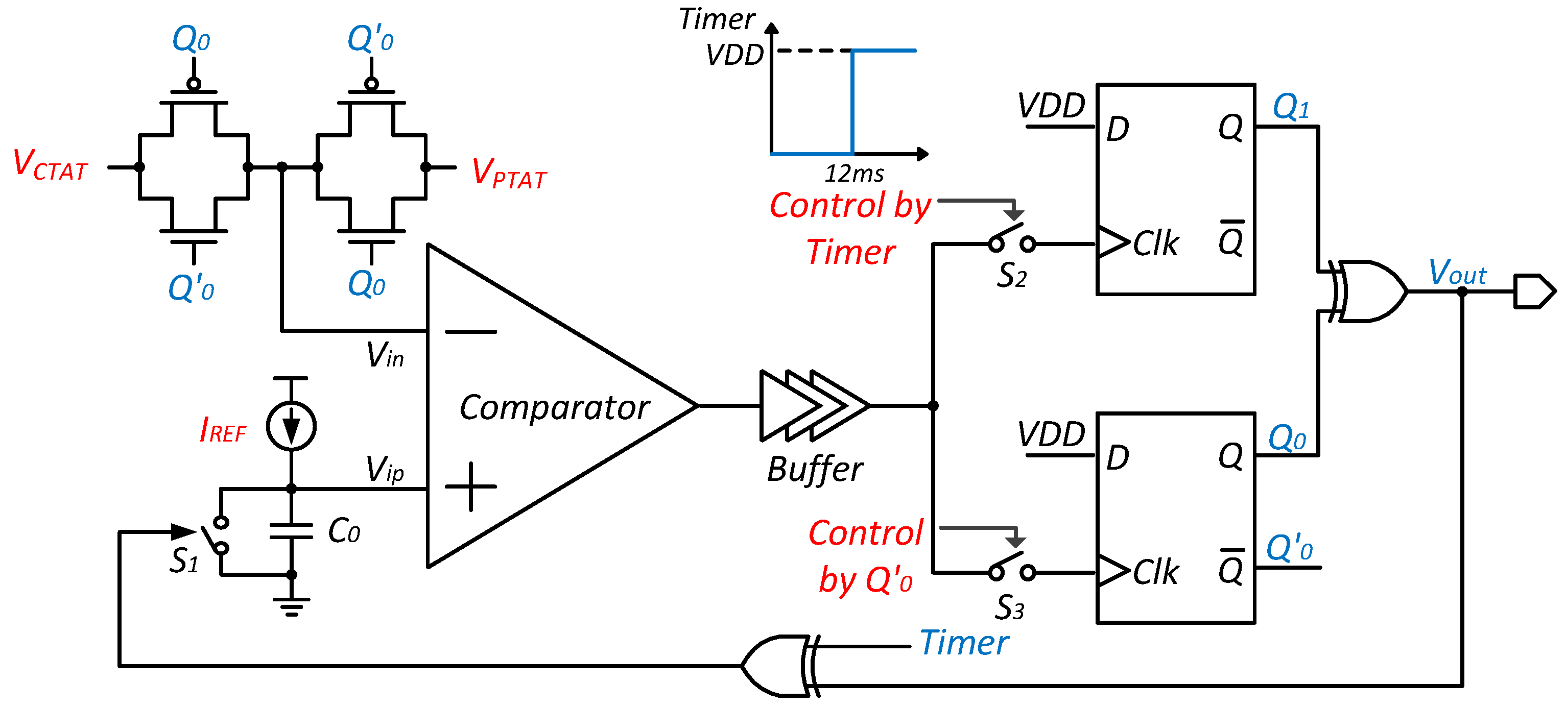
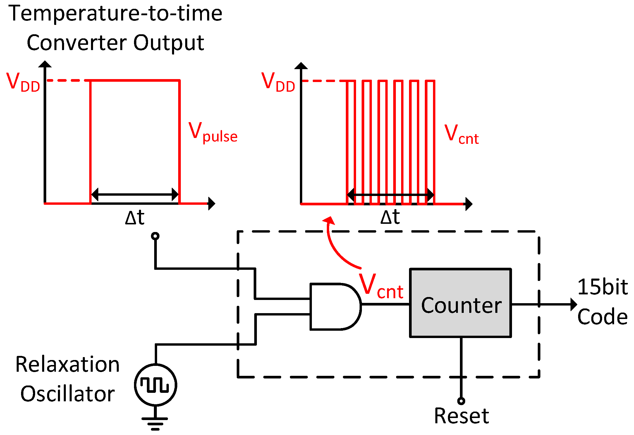
2. Architecture and Operation Principle
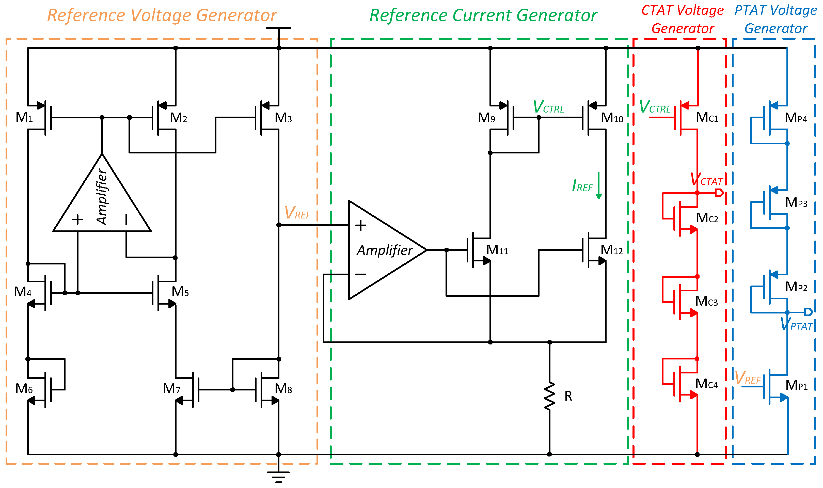
3. Circuit Implementation Details
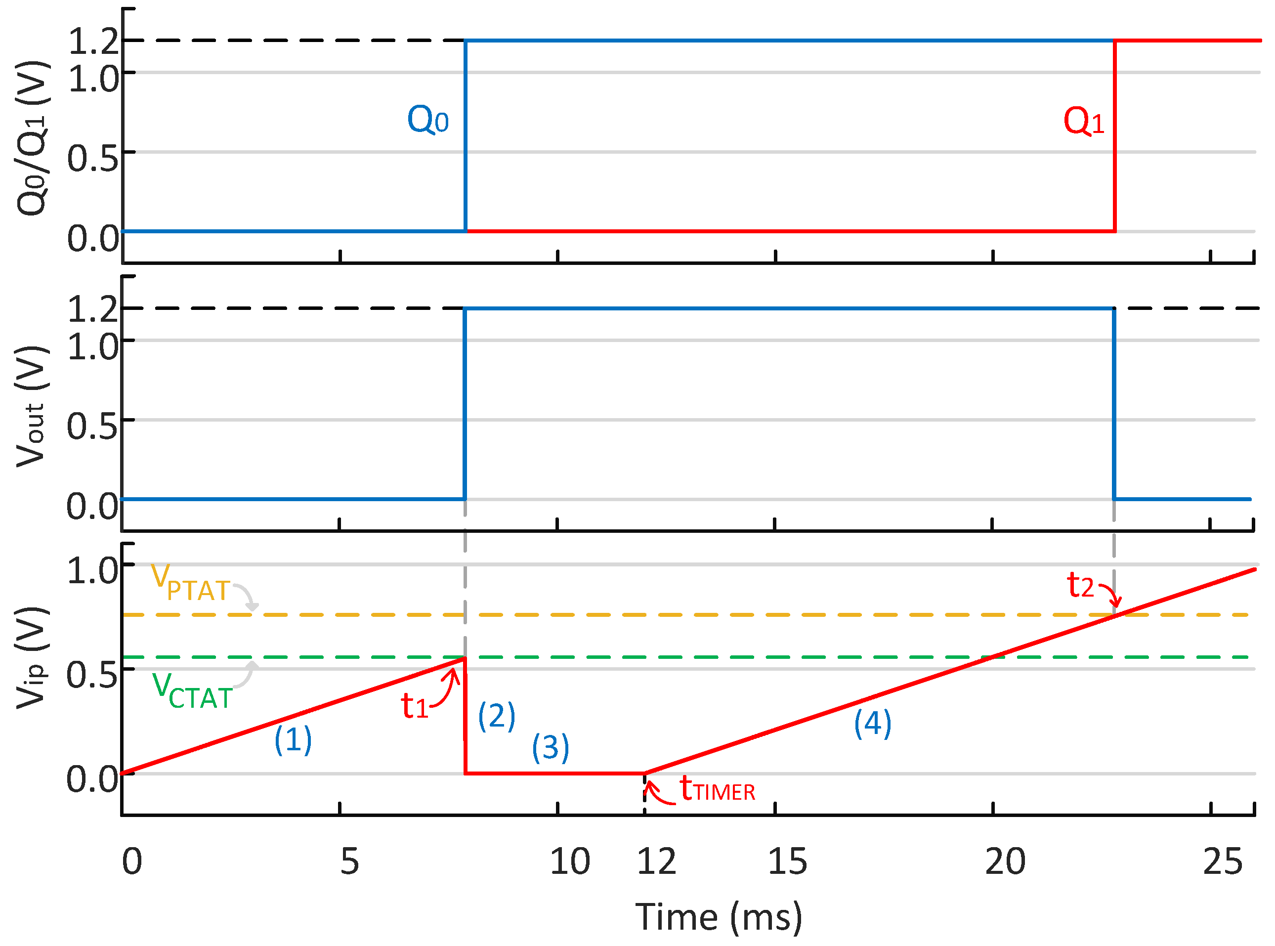
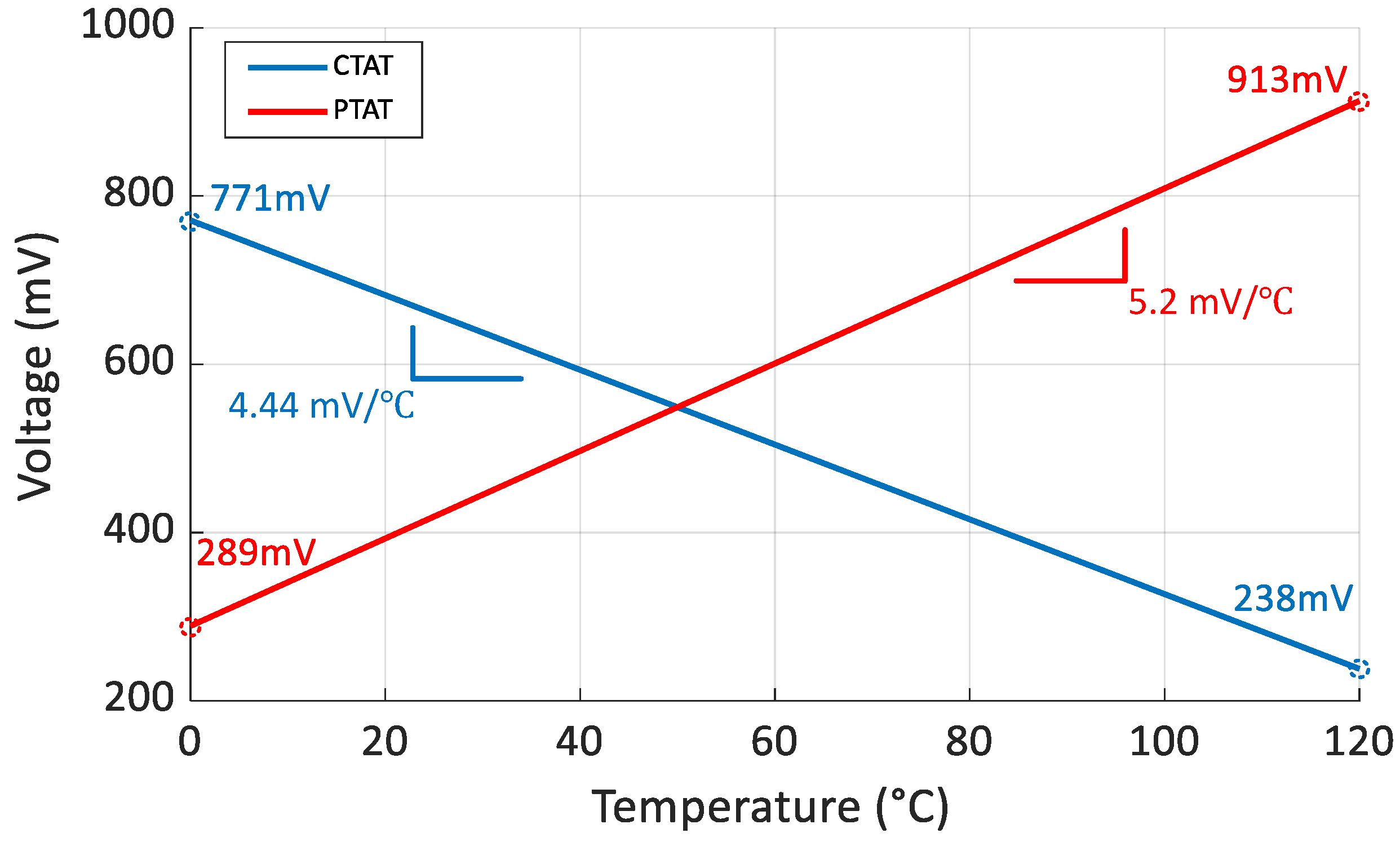
3.1. Temperature Sensing Core
3.2. Voltage-to-Time Converter
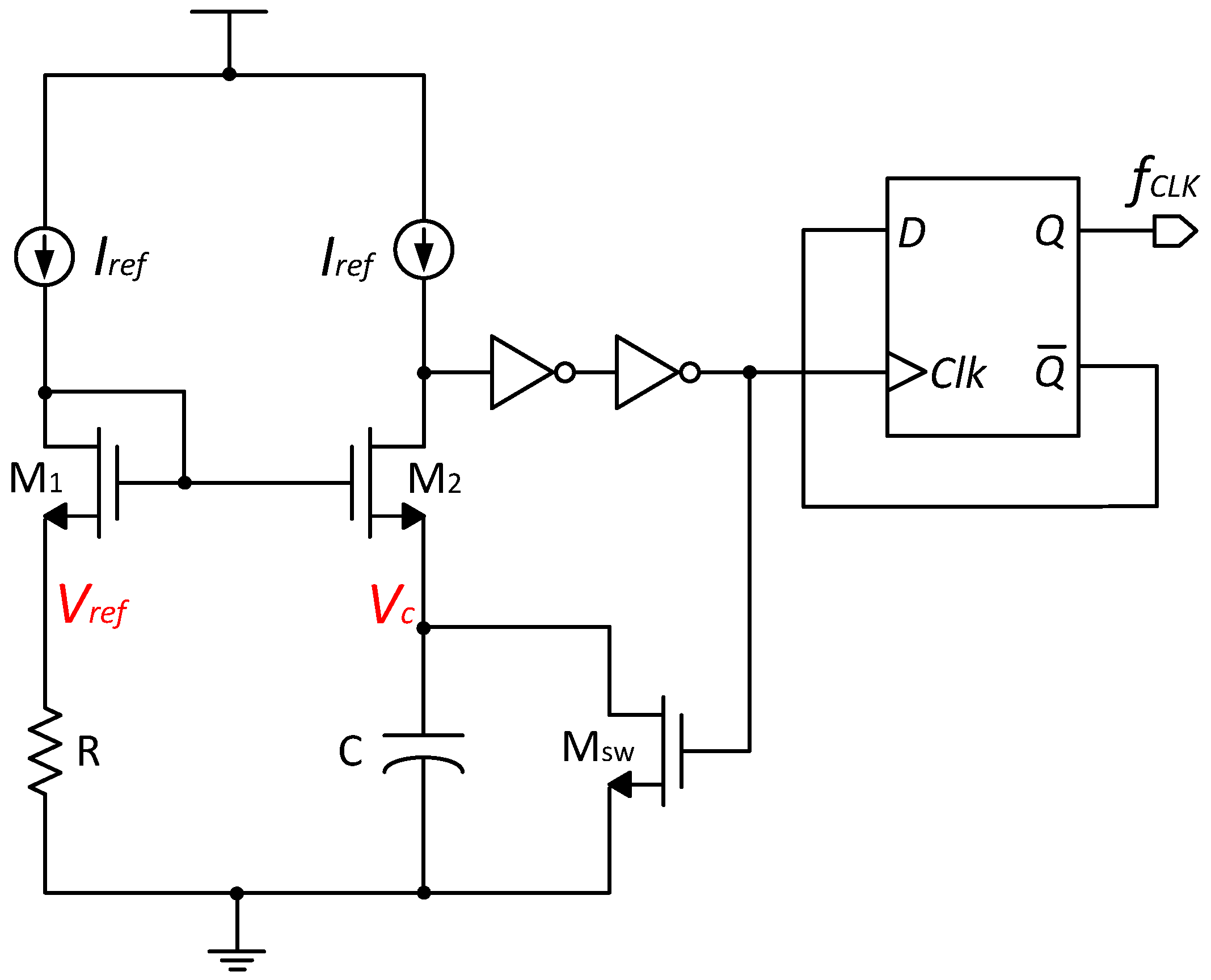
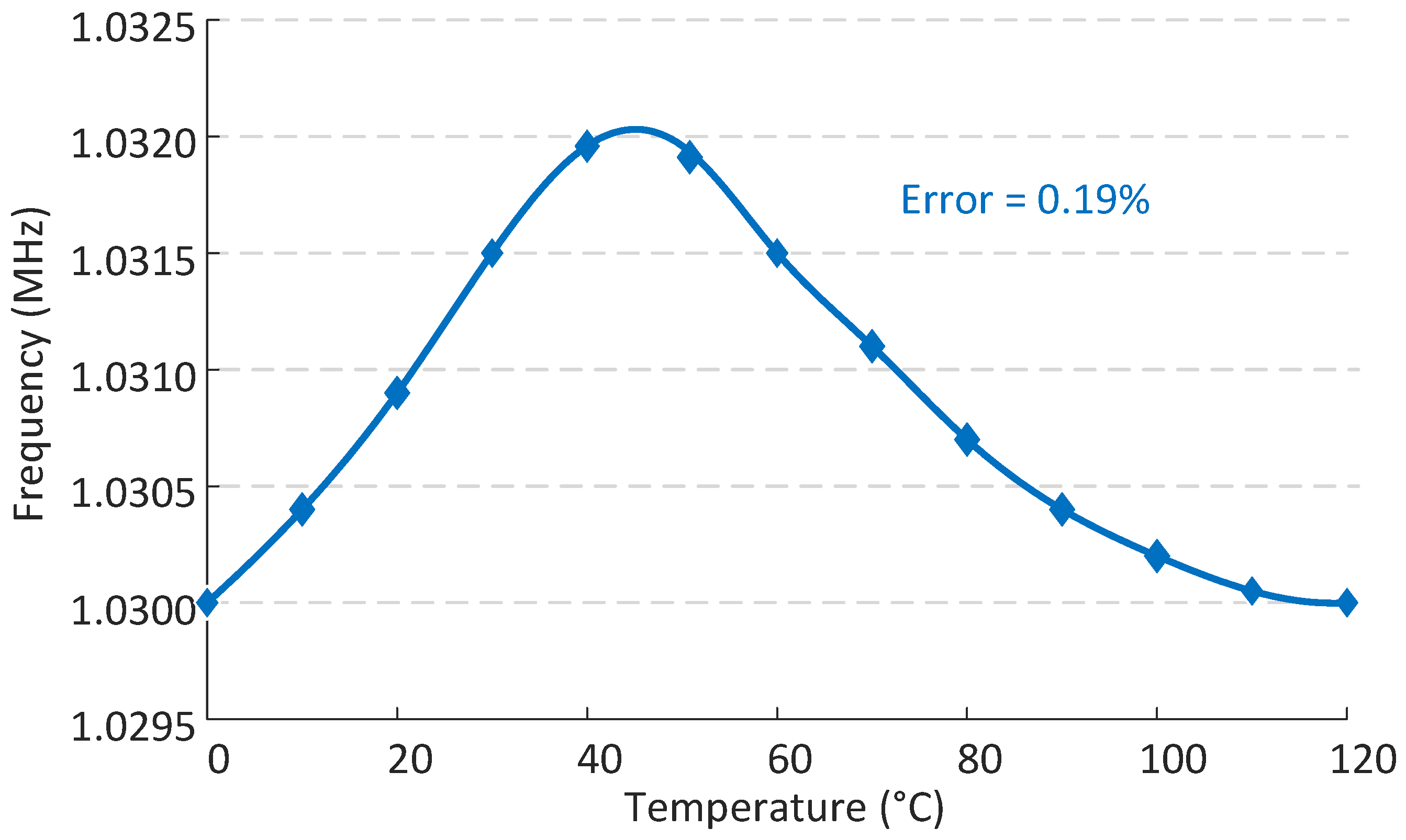
3.3. Relaxation Oscillator
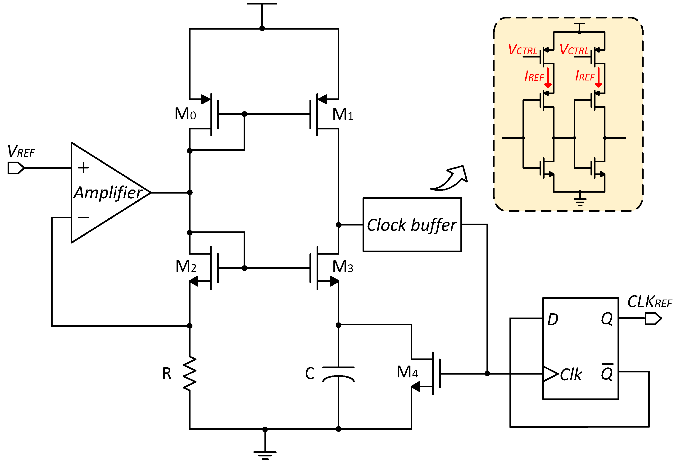
3.4. Time-to-Digital Converter
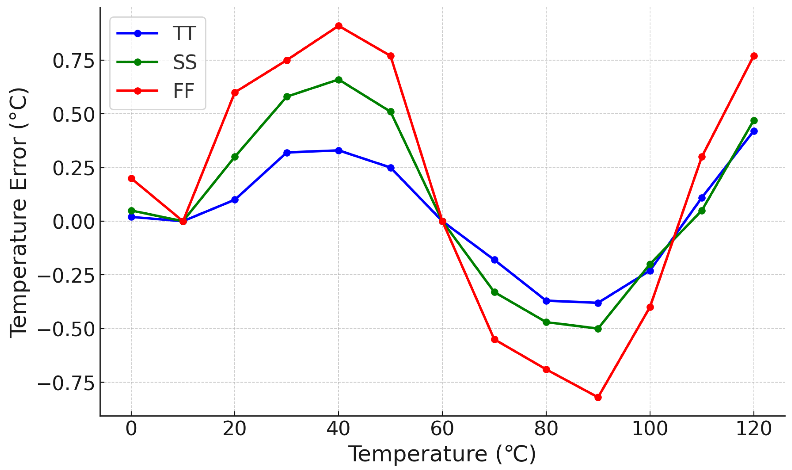
4. Simulation Results and Discussion
5. Conclusions
Author Contributions
Funding
Data Availability Statement
Conflicts of Interest
References
- Jain, A.; Jiang, H.; Pochet, C.; Hall, D.A. A 310 nW Temperature Sensor Achieving 9.8 mK Resolution Using a DFLL-Based Readout Circuit. IEEE Trans. Circuits Syst. II Express Briefs 2022, 69, 704–708. [Google Scholar] [CrossRef]
- Shen, Y.; Struijk, M.V.D.; Pelzers, K.; Li, H.; Cantatore, E.; Harpe, P. A 2.74 pJ/conversion 0.0018 mm2 Temperature Sensor with On-chip Gain and Offset Correction. In Proceedings of the ESSCIRC 2022-IEEE 48th European Solid State Circuits Conference (ESSCIRC), Milan, Italy, 19–22 September 2022; pp. 181–184. [Google Scholar] [CrossRef]
- Tang, Z.; Tan, N.N.; Shi, Z.; Yu, X.-P. A 1.2 V Self-Referenced Temperature Sensor with a Time-Domain Readout and a Two-Step Improvement on Output Dynamic Range. IEEE Sensors J. 2018, 18, 1849–1858. [Google Scholar] [CrossRef]
- Someya, T.; van Hoek, V.; Angevare, J.; Pan, S.; Makinwa, K. A 210 nW NPN-Based Temperature Sensor with an Inaccuracy of ±0.15 °C (3σ) From −15 °C to 85 °C Utilizing Dual-Mode Frontend. IEEE Solid-State Circuits Lett. 2022, 5, 272–275. [Google Scholar] [CrossRef]
- Sangalang, R.G.B.; Luo, S.-H.; Wang, C.-C. A High Resolution And Wide Range Temperature Detector Using 180-nm CMOS Process. In Proceedings of the 2023 International Conference on IC Design and Technology (ICICDT), Tokyo, Japan, 25–28 September 2023; pp. 64–67. [Google Scholar] [CrossRef]
- Law, M.K.; Bermak, A.; Luong, H.C. A Sub-μ W Embedded CMOS Temperature Sensor for RFID Food Monitoring Application. IEEE J. Solid-State Circuits 2010, 45, 1246–1255. [Google Scholar] [CrossRef]
- Someya, T.; Islam, A.K.M.M.; Sakurai, T.; Takamiya, M. An 11-nW CMOS Temperature-to-Digital Converter Utilizing Sub-Threshold Current at Sub-Thermal Drain Voltage. IEEE J. Solid-State Circuits 2019, 54, 613–622. [Google Scholar] [CrossRef]
- Chen, Y.; Jiao, Z.; Guan, W.; Sun, Q.; Wang, X.; Zhang, R.; Zhang, H. A +0.66/−0.73 °C Inaccuracy, 1.99-μW Time-Domain CMOS Temperature Sensor With Second-Order ΔΣ Modulator and on-Chip Reference Clock. IEEE Trans. Circuits Syst. I Regul. Pap. 2020, 67, 3815–3827. [Google Scholar] [CrossRef]
- Zhao, W.; Pan, R.; Ha, Y.; Yang, Z. A 0.4 V 280-nW frequency reference-less nearly all-digital hybrid domain temperature sensor. In Proceedings of the 2014 IEEE Asian Solid-State Circuits Conference (A-SSCC), KaoHsiung, Taiwan, 10–12 November 2014; pp. 301–304. [Google Scholar] [CrossRef]
- Makinwa, K. Smart Temperature Sensor Survey. Available online: http://ei.ewi.tudelft.nl/docs/TSensor_survey.xls (accessed on 7 May 2024).
- Pertijs, M.A.; Huijsing, J. Precision Temperature Sensors in CMOS Technology; Springer Science & Business Media: Berlin/Heidelberg, Germany, 2006. [Google Scholar]
- Souri, K.; Chae, Y.; Makinwa, K.A.A. A CMOS Temperature Sensor with a Voltage-Calibrated Inaccuracy of ±0.15 °C (3σ) from −55 °C to 125 °C. IEEE J. Solid-State Circuits 2013, 48, 292–301. [Google Scholar] [CrossRef]
- Xin, H.; Andraud, M.; Baltus, P.; Cantatore, E.; Harpe, P. A 174 pW–488.3 nW 1 S/s–100 kS/s All-Dynamic Resistive Temperature Sensor With Speed/Resolution/Resistance Adaptability. IEEE Solid-State Circuits Lett. 2018, 1, 70–73. [Google Scholar] [CrossRef]
- Pertijs, M.A.P.; Makinwa, K.A.A.; Huijsing, J.H. A CMOS smart temperature sensor with a 3σ inaccuracy of ±0.1 °C from −55 °C to 125 °C. IEEE J. Solid-State Circuits 2005, 40, 2805–2815. [Google Scholar] [CrossRef]
- Souri, K.; Chae, Y.; Thus, F.; Makinwa, K. 12.7 A 0.85 V 600 nW all-CMOS temperature sensor with an inaccuracy of ±0.4 °C (3σ) from −40 to 125 °C. In Proceedings of the 2014 IEEE International Solid-State Circuits Conference Digest of Technical Papers (ISSCC), San Francisco, CA, USA, 9–13 February 2014; pp. 222–223. [Google Scholar] [CrossRef]
- Wang, G.; Heidari, A.; Makinwa, K.A.A.; Meijer, G.C.M. An Accurate BJT-Based CMOS Temperature Sensor with Duty-Cycle-Modulated Output. IEEE Trans. Ind. Electron. 2017, 64, 1572–1580. [Google Scholar] [CrossRef]
- Chen, P.; Chen, C.C.; Tsai, C.C.; Lu, W.F. A time-to-digital-converter-based CMOS smart temperature sensor. IEEE J. Solid-State Circuits 2005, 40, 1642–1648. [Google Scholar] [CrossRef]
- Hwang, S.; Koo, J.; Kim, K.; Lee, H.; Kim, C. A 0.008 mm2 500 μW 469 kS/s Frequency-to-Digital Converter Based CMOS Temperature Sensor with Process Variation Compensation. IEEE Trans. Circuits Syst. I Regul. Pap. 2013, 60, 2241–2248. [Google Scholar] [CrossRef]
- Kim, J.; Kim, J.; Park, C.; Yang, M.; Jung, W. A Wide Range, Energy-Efficient Temperature Sensor Based on Direct Temperature–Voltage Comparison. IEEE Solid-State Circuits Lett. 2023, 6, 113–116. [Google Scholar] [CrossRef]
- Zeng, Y.; Cheng, J.; Chen, J.; Huang, W. A +0.35 °C/−0.22 °C Inaccuracy CMOS-Based Temperature Sensor for IoT Applications. In Proceedings of the 2023 IEEE 66th International Midwest Symposium on Circuits and Systems (MWSCAS), Tempe, AZ, USA, 6–9 August 2023; pp. 157–161. [Google Scholar] [CrossRef]
- Chen, P.; Hu, Y.-J.; Liou, J.-C.; Ren, B.-C. A 486k S/s CMOS time-domain smart temperature sensor with −0.85 °C/0.78 °C voltage-calibrated error. In Proceedings of the 2015 IEEE International Symposium on Circuits and Systems (ISCAS), Lisbon, Portugal, 24–27 May 2015; pp. 2109–2112. [Google Scholar] [CrossRef]
- Cao, F.; Jiang, M.; Zhang, Z. A low-temperature drift current-mode relaxation oscillator with feed-forward period control. In Proceedings of the 2023 8th International Conference on Integrated Circuits and Microsystems (ICICM), Nanjing, China, 20–23 October 2023; pp. 150–154. [Google Scholar] [CrossRef]
- Mohammed, M.; Abugharbieh, K.; Abdelfattah, M.; Kawar, S. Design methodology for MOSFET-based voltage reference circuits implemented in 28nm CMOS technology. AEU-Int. J. Electron. Commun. 2016, 70, 568–577. [Google Scholar] [CrossRef]
- Babayan-Mashhadi, S.; Lotfi, R. Analysis and Design of a Low-Voltage Low-Power Double-Tail Comparator. IEEE Trans. Very Large Scale Integr. (VLSI) Syst. 2014, 22, 343–352. [Google Scholar] [CrossRef]
- Chiang, Y.-H.; Liu, S.-I. A Submicrowatt 1.1-MHz CMOS Relaxation Oscillator With Temperature Compensation. IEEE Trans. Circuits Syst. II Express Briefs 2013, 60, 837–841. [Google Scholar] [CrossRef]
- Wang, X.; Wang, P.-H.P.; Cao, Y.; Mercier, P.P. A 0.6 V 75 nW All-CMOS Temperature Sensor With 1.67 m °C/mV Supply Sensitivity. IEEE Trans. Circuits Syst. I Regul. Pap. 2017, 64, 2274–2283. [Google Scholar] [CrossRef]
- Park, J.-H.; Hwang, J.-H.; Shin, C.; Kim, S.-J. A BJT-Based Temperature-to-Frequency Converter With ±1 °C (3σ) Inaccuracy From −40 °C to 140 °C for On-Chip Thermal Monitoring. IEEE J. Solid-State Circuits 2022, 57, 2909–2918. [Google Scholar] [CrossRef]
- Li, J.; Lin, Y.; Ning, N.; Yu, Q. A +0.44 °C/−0.4 °C Inaccuracy Temperature Sensor With Multi-Threshold MOSFET-Based Sensing Element and CMOS Thyristor-Based VCO. IEEE Trans. Circuits Syst. I Regul. Pap. 2021, 68, 1102–1113. [Google Scholar] [CrossRef]
- Kim, J.; Lee, S.; Lee, M. A 0.9 V Self-Referenced Resistor-Based Temperature Sensor With −0.62/+0.81 °C (3σ) Inaccuracy. IEEE Trans. Circuits Syst. II Express Briefs 2023, 70, 4319–4323. [Google Scholar] [CrossRef]
- Wei, R.; Bao, X. A low power energy-efficient precision CMOS temperature sensor. Micromachines 2018, 9, 257. [Google Scholar] [CrossRef] [PubMed]


| Paper | JSSC [27] | TCAS-I [8] | TCAS-I [28] | TCAS-II [1] | TCAS-II [29] | MDPI [30] | This Work |
|---|---|---|---|---|---|---|---|
| Year | 2022 | 2020 | 2021 | 2022 | 2023 | 2018 | 2024 |
| Technology (nm) | 110 | 180 | 130 | 65 | 28 | 180 | 180 |
| Type | BJT | MOSFET | MOSFET | Res | Res | BJT | MOSFET |
| Supply Voltage (V) | 1.35∼2 | 1.8 | 0.95 | 0.9 | 0.9 | 1.8 | 1.2 |
| Temperature Range (°C) | −40∼140 | −20∼80 | 0∼80 | −5∼95 | −40∼100 | 0∼100 | 0∼120 |
| Resolution (°C) | 0.144 | 0.1 | 0.1 | 0.0098 | 0.0565 | 0.01 | 0.0071 |
| Conversion Time (ms) | 0.8 | 25 | 59 | 10 | 0.404 | 3.4 | 26 |
| Inaccuracy (°C) | +1/−1 | +0.66/−0.73 | +0.44/−0.4 | +1.8/−1.6 | +0.81/−0.62 | +0.2/−0.2 | +0.43/−0.38 |
| Relative Inaccuracy 1 (%) | 1.11 | 1.39 | 1.05 | 3.4 | 1.02 | 0.4 | 0.675 |
| Power 2 (W) | 3.1 | 1.99 | 0.196 | 0.31 | 123.5 | 11.2 | 1.48 |
| Energy/Conversion (nJ) | 2.48 | 49.75 | 11.56 | 3.1 | 49.9 | 38 | 38.39 |
| Resolution FOM 3 (nJ · K2) | 0.0514 | 0.4975 | 0.1156 | 0.000297 | 0.159 | 0.0038 | 0.0019 |
Disclaimer/Publisher’s Note: The statements, opinions and data contained in all publications are solely those of the individual author(s) and contributor(s) and not of MDPI and/or the editor(s). MDPI and/or the editor(s) disclaim responsibility for any injury to people or property resulting from any ideas, methods, instructions or products referred to in the content. |
© 2024 by the authors. Licensee MDPI, Basel, Switzerland. This article is an open access article distributed under the terms and conditions of the Creative Commons Attribution (CC BY) license (https://creativecommons.org/licenses/by/4.0/).
Share and Cite
Sun, Y.; Cheng, J.; Luo, Z.; Zeng, Y. A Sub-0.01 °C Resolution All-CMOS Temperature Sensor with 0.43 °C/−0.38 °C Inaccuracy and 1.9 pJ · K2 Resolution FoM for IoT Applications. Micromachines 2024, 15, 1132. https://doi.org/10.3390/mi15091132
Sun Y, Cheng J, Luo Z, Zeng Y. A Sub-0.01 °C Resolution All-CMOS Temperature Sensor with 0.43 °C/−0.38 °C Inaccuracy and 1.9 pJ · K2 Resolution FoM for IoT Applications. Micromachines. 2024; 15(9):1132. https://doi.org/10.3390/mi15091132
Chicago/Turabian StyleSun, Yixiao, Jie Cheng, Zhizhong Luo, and Yanhan Zeng. 2024. "A Sub-0.01 °C Resolution All-CMOS Temperature Sensor with 0.43 °C/−0.38 °C Inaccuracy and 1.9 pJ · K2 Resolution FoM for IoT Applications" Micromachines 15, no. 9: 1132. https://doi.org/10.3390/mi15091132