Abstract
As the competition intensifies in enhancing the integration and performance of integrated circuits, in accordance with the famous Moore’s Law, higher performance and smaller size requirements are imposed on the dielectric layers in electronic devices. Compared to vacuum methods, the production cost of preparing dielectric layers via solution methods is lower, and the preparation cycle is shorter. This paper utilizes a low-temperature self-exothermic reaction based on the solution method to prepare high-performance Al2O3 dielectric thin films that are compatible with flexible substrates. In this paper, we first established two non-self-exothermic systems: one with pure aluminum nitrate and one with pure aluminum acetylacetonate. Additionally, we set up one self-exothermic system where aluminum nitrate and aluminum acetylacetonate were mixed in a 1:1 ratio. Tests revealed that the leakage current density and dielectric constant of the self-exothermic system devices were significantly optimized compared to the two non-self-exothermic system devices, indicating that the self-exothermic reaction can effectively improve the quality of the dielectric film. This paper further established two self-exothermic systems with aluminum nitrate and aluminum acetylacetonate mixed in 2:1 and 1:2 ratios, respectively, for comparison. The results indicate that as the proportion of aluminum nitrate increases, the overall dielectric performance of the devices improves. The best overall performance occurs when aluminum nitrate and aluminum acetylacetonate are mixed in a ratio of 2:1: The film surface is smooth without cracks; the surface roughness is 0.747 ± 0.045 nm; the visible light transmittance reaches up to 98%; on the basis of this film, MIM devices were fabricated, with tested leakage current density as low as 1.08 × 10⁻⁸ A/cm2 @1 MV and a relative dielectric constant as high as 8.61 ± 0.06, demonstrating excellent electrical performance.
1. Introduction
With the advanced development of integrated circuits, there is a growing demand for thinner dielectric layers in electronic components [1,2,3]. However, when the thickness of the amorphous silicon dielectric layer is reduced to below 3 nm, the gate leakage current caused by direct tunneling can reach up to 1 A/cm2 [4]. To reduce leakage current and increase the thickness of the dielectric layer, various high-k dielectric materials have been used, including Al2O3, HfO2, ZnO, and ZrO2 [5,6,7,8,9]. They also offer advantages such as high mobility, high transparency, and suitability for flexible substrates [10,11,12].
The preparation method of high-k gate dielectric layers is the classical vacuum method [13,14,15,16], resulting in excellent film uniformity and high quality. However, these equipment options are characterized by high costs and lengthy experimental durations. Therefore, in order to achieve low-cost, rapid, and high-quality preparation of dielectric layers, the solution method has attracted widespread attention and research [17,18,19,20]. However, in the process of film preparation using solution methods, in order to achieve the removal of organic ligands and densification of the film, the annealing temperature is typically higher than 400 °C or even higher [21,22]. This limits the preparation of dielectric films on flexible substrates.
Recently, many new low-temperature solution methods for preparing dielectric layers have been studied. Wangying Xu and her team prepared Al2O3 dielectric films using a ‘aqueous route’ with annealing at 250 °C [23]. The leakage current density is 2.9 × 10⁻⁷ A/cm2@1 MV/cm, the dielectric constant is 8.6, and the breakdown field strength is greater than 2.5 MV/cm. Jeong-Wan Jo employed a high-density UV (DUV) treatment-assisted exothermic process using low-pressure mercury lamps to prepare Al2O3/ZrO2 dielectric layers at 180 °C [24]. The leakage current density was reduced to 4.68×10⁻⁹ A/cm2@1 MV/cm. Sumei Wang used infrared irradiation for 40 min to induce the low-temperature decomposition of AlCl3 precursor solution into Al2O3 films, achieving a high dielectric constant [7,8] and a low leakage current (3.5 × 10⁻⁸ A/cm2@1 MV/cm) [25]. A breakdown field strength greater than 3 MV/cm was obtained. These low-temperature solution methods share a common characteristic, which is the utilization of photo-irradiation or other methods to assist the exothermic process based on exothermic reaction. A drawback is the need for constant adjustment of the power and wavelength of auxiliary equipment to achieve optimal settings.
In this paper, we utilize a low-temperature self-exothermic reaction based on the solution method to prepare high-performance Al2O3 dielectric thin films. In the exothermic reaction, metal nitrates act as strong oxidants, while acetylacetonates serve as strong reductants. The mixed sample undergoes a spontaneous and vigorous redox reaction upon reaching a relatively low annealing temperature, generating a substantial amount of heat to compensate for the energy required for the formation of M-O-M bonds, thereby producing high-performance dielectric films. This exothermic process requires only a constant-temperature heating device and no additional auxiliary equipment, and the low annealing temperature allows compatibility with flexible substrates and reduces energy consumption. This low-temperature solution method offers advantages such as low cost, adjustable composition, safety, and the ability to produce large-area films [26,27,28]. Here, this paper proposes a self-exothermic reaction, distinct from traditional exothermic reactions, where the process only requires the mixing of metal precursors containing fuel ligands and oxidant ligands without the need for additional fuel; this simple precursor solution composition is easy to control and replicate, facilitating the preparation of stable dielectric layers and MIM (Metal–Insulator–Metal) devices.
2. Experiment
2.1. Synthesis of Precursor Solution
All reagents, including aluminum nitrate hydrate (Al(NO3)3·9H2O, AlNO), aluminum triacetylacetone (C15H21O6Al, AlAC) and N,N-Dimethylformamide (C3H7NO, DMF), were purchased from Merck and required no further purification.
The preparation of the self-exothermic precursor solution is as follows: The total concentration is controlled at 0.2 M, which can be calculated as follows:
c (AlNO) + c (AlAC) = 0.2 M
Five samples of precursor solutions were prepared by mixing AlNO and AlAC in different ratios, as shown in Table 1. The solvent chosen is DMF. It was stirred magnetically for 24 h, followed by aging for 4 h at rest. Subsequently, the precursor solution was filtered using a 0.22 μm organic-phase syringe filter to obtain the solution for spin-coating.

Table 1.
Proportion of precursor system components and naming of precursor systems.
In this paper, the five samples of precursor systems will be simplified, with their names shown in Table 1.
2.2. Dielectric Film Fabrication
ITO glass substrates were subjected to ultrasonic cleaning in a sequence of deionized water/isopropanol/deionized water/isopropanol, then dried at 80 °C for 12 h. Prior to spin-coating, the substrates were UV-treated for 20 min. Subsequently, 40 μL of the precursor solution was spin-coated on the substrates at 500 r/min for 5 s and 5000 r/min for 30 s. Finally, dielectric films were pre-annealed at 80 °C for 10 min and post-annealed at 185 °C for 1 h.
The weight and heat changes of the precursor solution were measured using a Thermogravimetric Analyzer (TG, DZ-TGA101, Nanjing, China) and Differential Scanning Calorimetry (DSC, DZ-DSC300C, Nanjing, China). The surface tension of the precursor solution was measured using Attension Theta Lite (TL200, BiolinScientific, Gothenburg, Sweden). The surface morphology of the dielectric films was observed using Laser Scanning Confocal Microscopy (LSCM, OLS50-CB, Tokyo, Japan) and Atomic Force Microscopy (AFM, BY3000, Nano Instruments, Guangzhou, China). The thickness, density, and roughness of the films were fitted using an X-ray Reflectometer (XRR, PANalytical Empyrean, Almelo, The Netherlands). The optical properties were studied using an Ultraviolet-Visible Spectrophotometer (UV-Vis, UV-3600 Shimadzu, Kyoto, Japan). The phase structure of the films was analyzed using an X-ray Diffractometer (XRD, PANalytical Empyrean, Almelo, The Netherlands), and the functional groups were characterized using Fourier Transform Infrared Spectroscopy (FTIR, ATR Accessory, Nexus, Madison, WI, USA).
2.3. MIM Device Fabrication
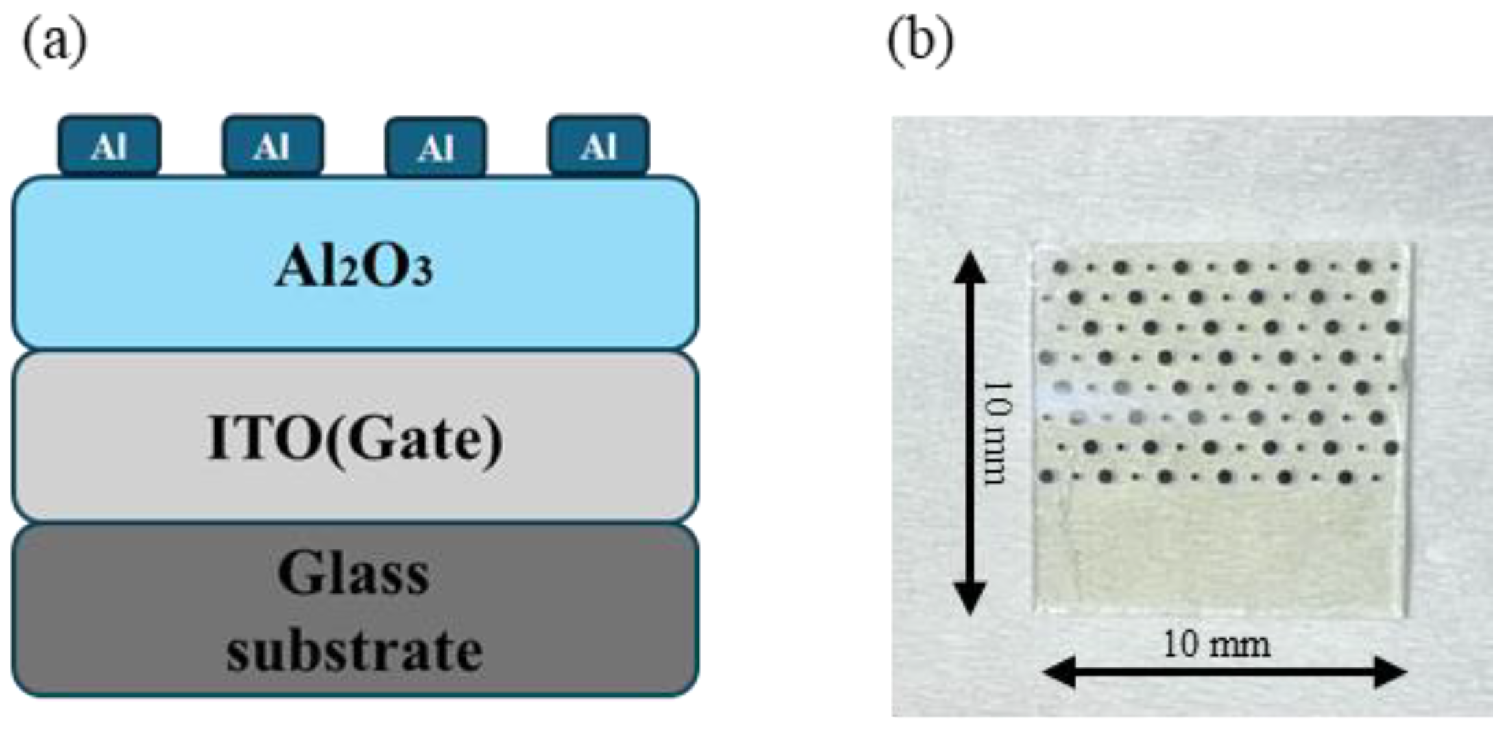
The electrical properties of dielectric films are typically characterized by preparing MIM devices [29]. MIM devices were fabricated with Al2O3 as the dielectric layer, as shown in Figure 1. Al electrodes were thermally deposited on the surface of the dielectric film, with an electrode area of 1.256 × 10⁻³ cm2. The current–voltage (I–V), capacitance–voltage (C-V), and capacitance–frequency (C-F) characteristics of MIM devices were measured using the semiconductor parameter analyzer (Primarius FS-Pro, Shanghai, China). In order to ensure the authenticity and universality of the experimental data, three test samples were prepared for each component, and two different test points were characterized for each sample. If the test results obtained are close, it indicates good uniformity of the film.
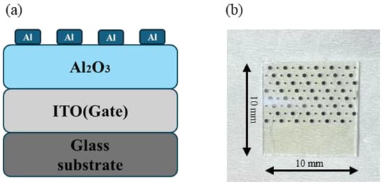
Figure 1.
MIM device: (a) schematic; (b) photo.
3. Result and Discussion
3.1. Surface Tension Tests Results
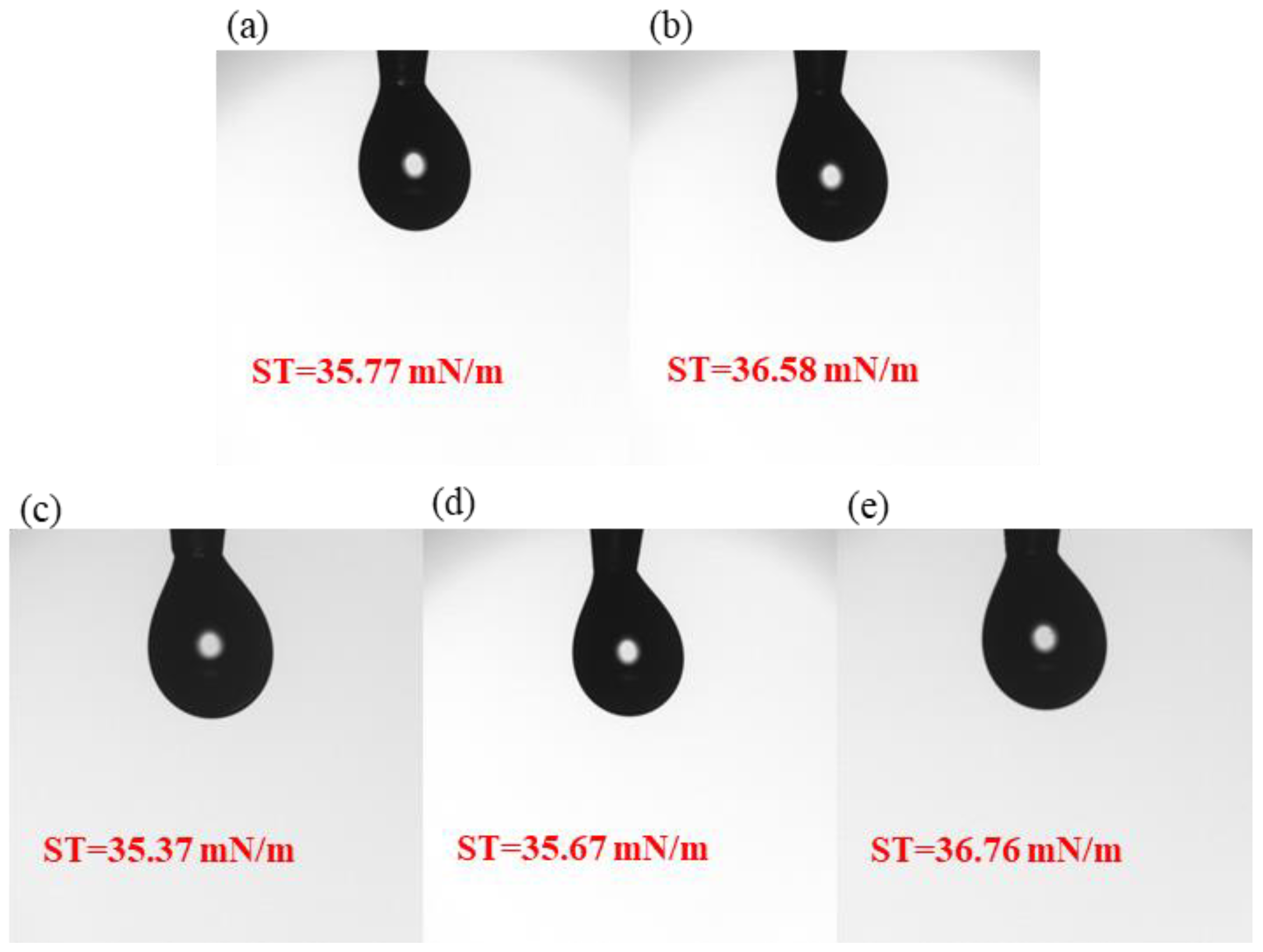
The surface tension tests of the five precursor solutions are shown in Figure 2. The results show that all five samples of precursor solutions have relatively average surface tension. The surface tensions of samples S1, S2, S3, S4 and S5 studied in this paper are 35.77 mN/m, 36.58 mN/m, 35.37 mN/m, 35.67 mN/m, and 36.76 mN/m, aligning with spin-coating thin films.
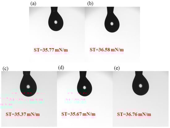
Figure 2.
Surface tension: (a) S1; (b) S2; (c) S3; (d) S4; (e) S5.
3.2. TG-DSC Test Analysis
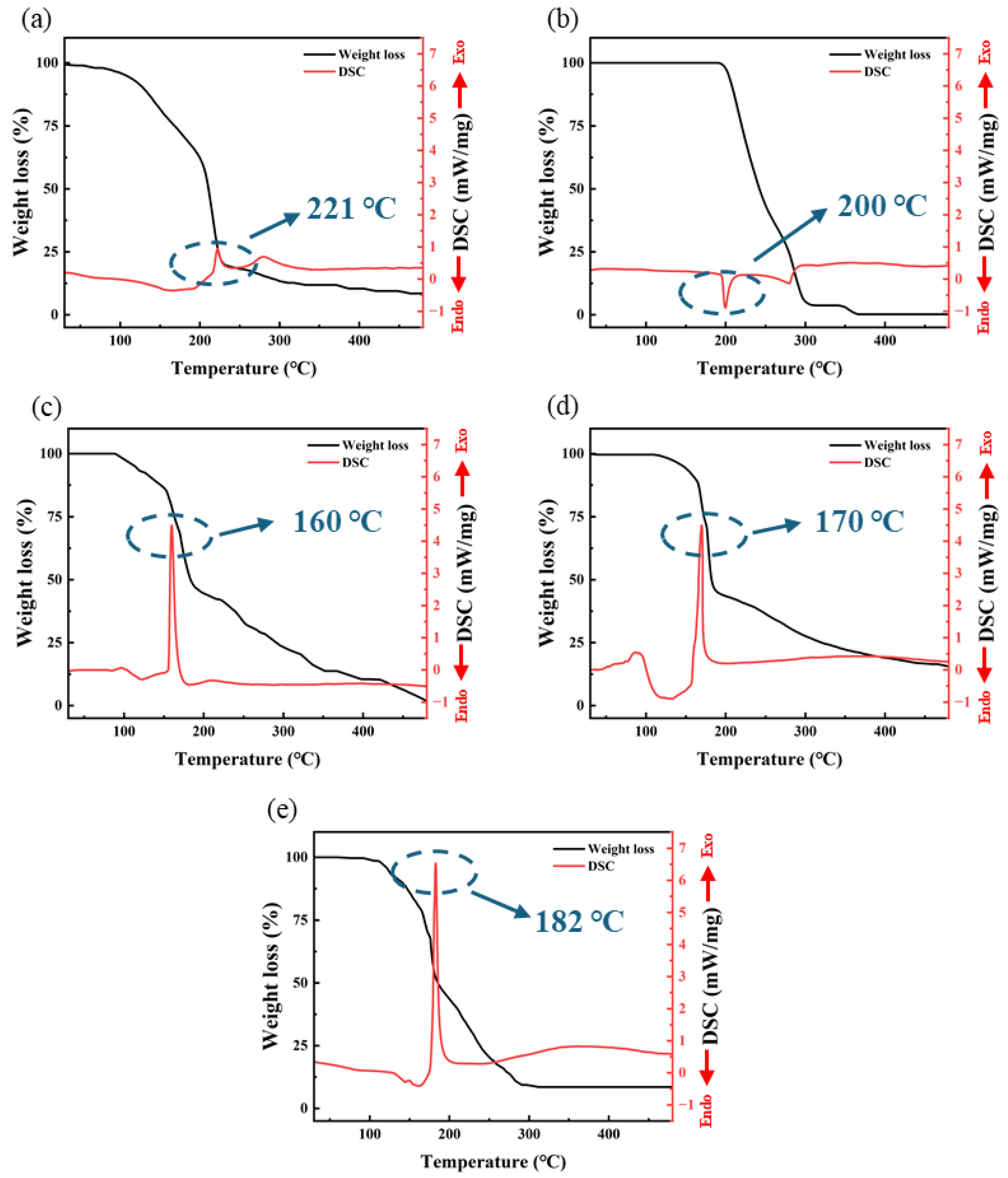
The TG-DSC test results are shown in Figure 3. From the results, it is evident that three groups of self-exothermic precursor samples exhibit a distinctly different thermal behavior compared to the other two non-self-exothermic precursor samples. S3, S4, and S5 exhibit intense exothermic behavior near 160~180 °C. In contrast, S1 and S2 show no significant exothermic activity throughout the entire temperature range (30~500 °C).
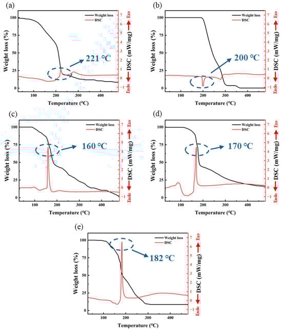
Figure 3.
The TG-DSC test curve: (a) S1; (b) S2; (c) S3; (d) S4; (e) S5.
The decomposition temperature of Al(NO3)3 is around 200 °C, resulting in the formation of Al2O3 and the release of a large amount of gasses such as NO, NO2, and O2 [30]. From Figure 3a, it can be observed that S1 experiences a sharp decrease in mass around 220 °C, corresponding to the production of a large amount of gas during the decomposition reaction. Therefore, the exothermic behavior of S1 around 221 °C is likely due to the decomposition reaction. S2 exhibits a weak endothermic peak around 200 °C, which is due to the melting and sublimation of AlAC at this temperature, with a significant mass loss resulting from the evaporation of a substantial amount of material.
However, three samples of different self-exothermic precursors exhibited a significant exothermic peak at 160~180 °C. S3, S4 and S5, respectively, exhibited sharp exothermic peaks around 160 °C, 170 °C, and 182 °C, with exothermic intensities of 4.46 mW/mg, 4.48 mW/mg and 6.53 mW/mg, respectively. Each exothermic peak corresponds to a significant mass loss, which is due to the generation of large amounts of gas from redox reactions. The temperature corresponding to the exothermic peak increases with an increase in the proportion of AlAC; at the same time, the exothermic intensity also increases. Additionally, S4 exhibited a broad endothermic peak around 138 °C. This is due to the residual DMF solvent in the sample boiling and absorbing heat at this temperature.
From the DSC data of S1 and S2, it can be observed that neither S1 nor S2 exhibits significant exothermic behavior below 200 °C. This indicates that the exothermic behavior observed in S3, S4, and S5 in the range of 160~185 °C is not due to a single substance of AlNO or AlAC but rather results from the redox reaction between AlNO and AlAC: at this temperature, the nitrate ions in AlNO, along with a small amount of oxygen generated from the decomposition of nitrate ions, act as strong oxidants. They undergo vigorous redox reactions with AlAC, acting as a reducing agent, producing a large amount of heat, resulting in the formation of Al2O3 and a substantial quantity of gas. Significant mass loss observed in the TGA test results is attributable to this reaction. The heat provided by this rapid and intense exothermic reaction may promote the formation of M-O-M bonds and the removal of organic ligands, offering the potential for the preparation of high-performance dielectric layers at low temperatures.
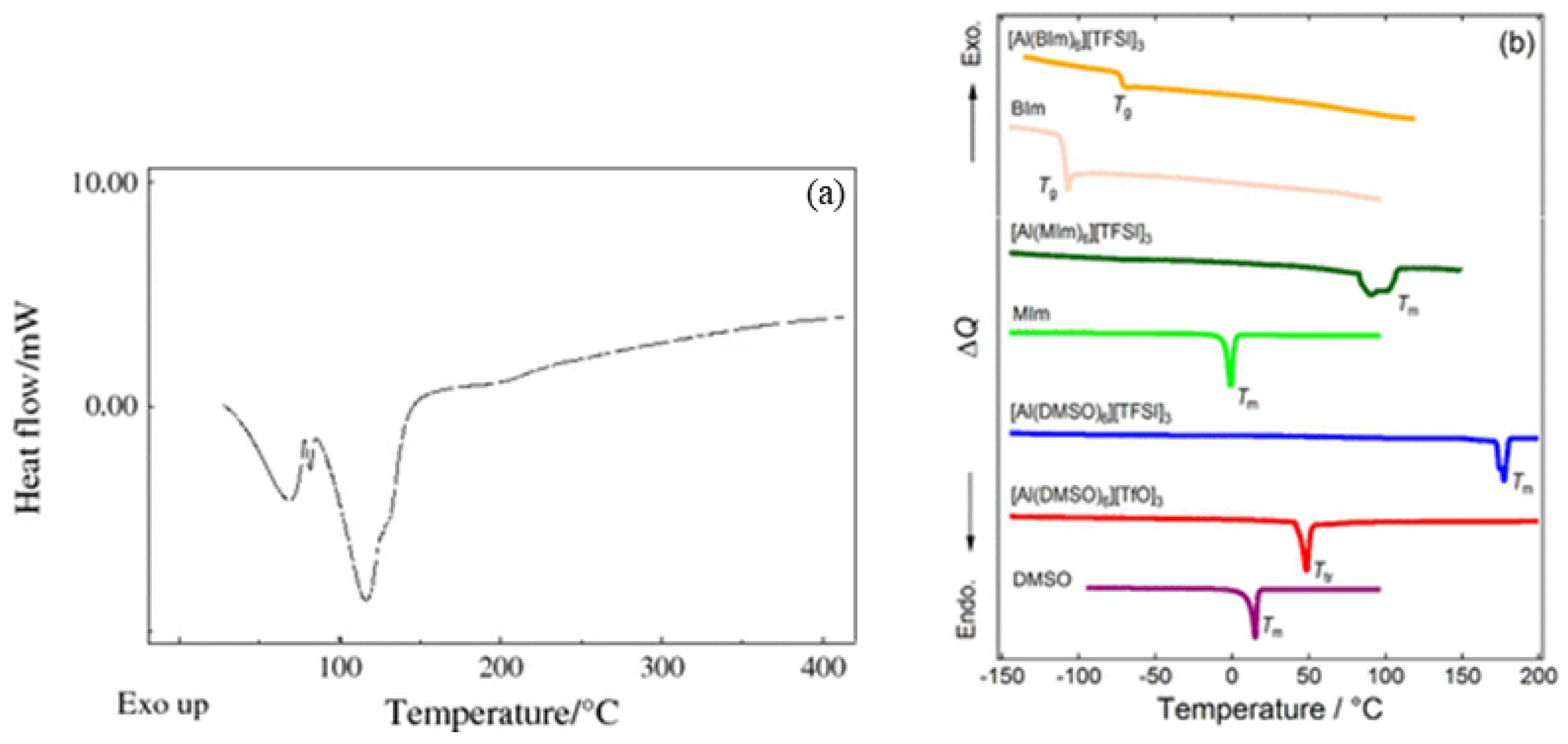
In Figure 4, DSC data for other aluminum salts are provided for comparison. As seen in Figure 4a, a prominent endothermic peak appears around 130 °C, which is attributed to the removal of H2O in sample Al(NO3)3·8H2O [30]. In contrast, no similar endothermic peak appears around 130 °C in Figure 3a, as the DSC samples in this article were first dissolved in DMF and then dried to form solid samples, so the H2O was already dissolved in the DMF. However, none of the aluminum salts in Figure 4 exhibit significant exothermic peaks, which further indicates that the prominent exothermic peaks observed in Figure 3c–e are not caused by a single aluminum salt. Instead, they are due to the redox reactions between AlNO and AlAC, which release a substantial amount of heat.
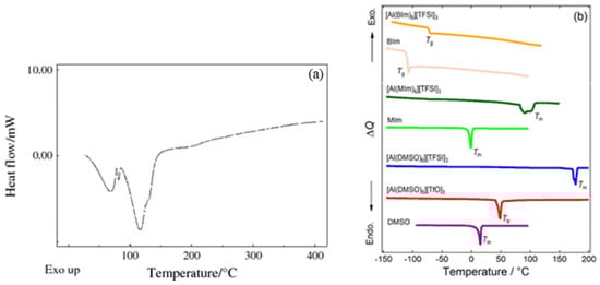
Figure 4.
Comparison of DSC curves for different aluminum salts: (a) DSC curve of Al(NO3)3·8H2O [31]; (b) DSC traces of [Al(L)6]X3 (L = DMSO, MIm, or BIm; X = TFSI or TfO) with the pure ligands as references. Tm, Ttr, and Tg denote melting points, solid-solid phase transition temperatures, and glass transition temperatures, respectively [32].
3.3. Surface Morphology Analysis
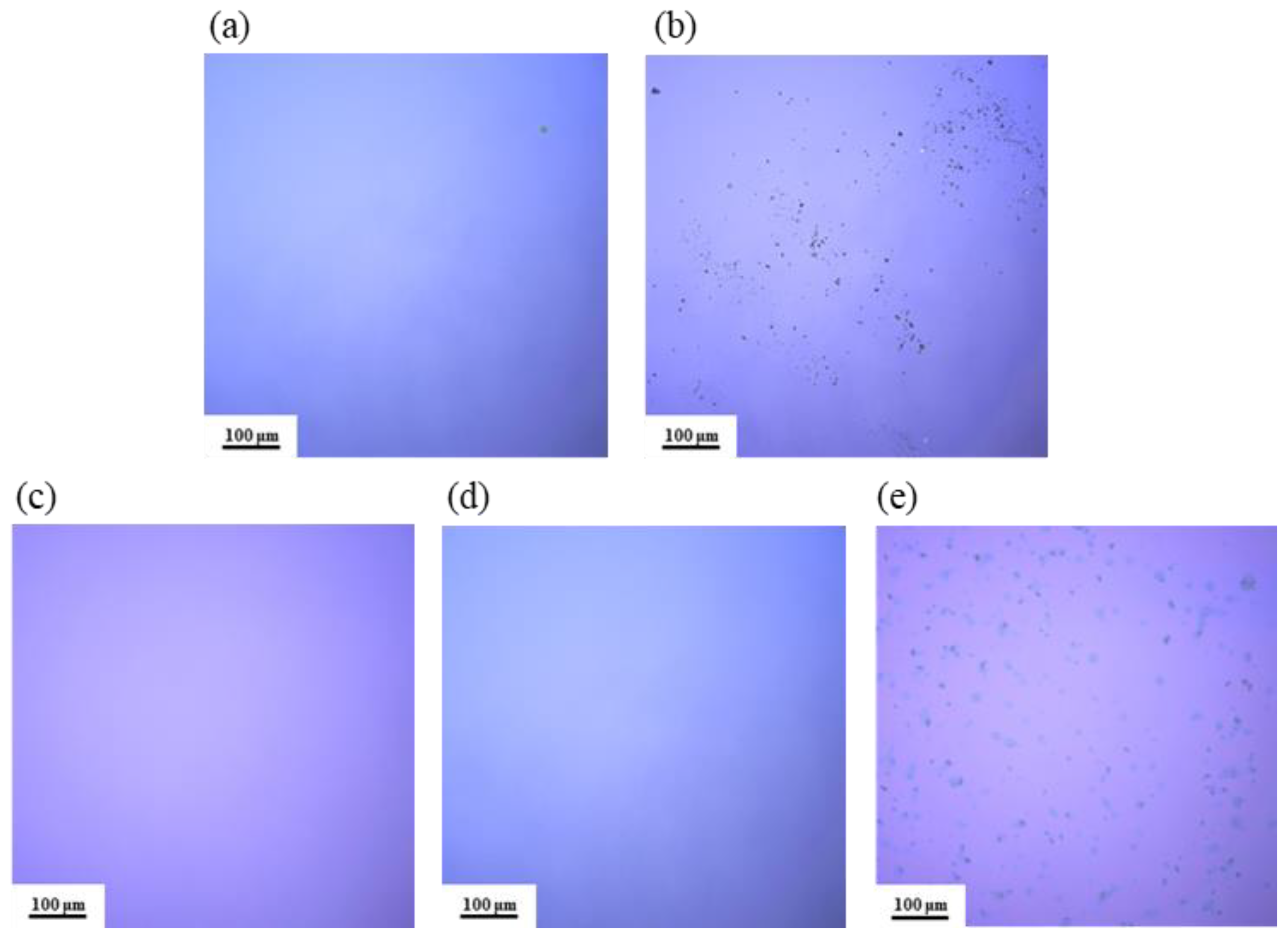
As shown in Figure 5, the surface morphology of different film samples was observed using LSCM. From Figure 5a,c,d, the film surfaces are smooth and uniform, with no visible cracks or black particles. In contrast, Figure 5b,e clearly shows a significant distribution of black particles on the film surfaces, leading to an uneven texture. This may be due to the low solubility of AlAC in the DMF solvent: as the temperature increases, AlAC precipitates out before it has a chance to react, resulting in the formation of crystalline particles on the film surface.
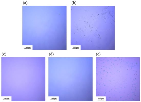
Figure 5.
LSCM images of Al2O3 films: (a) S1; (b) S2; (c) S3; (d) S4; (e) S5.
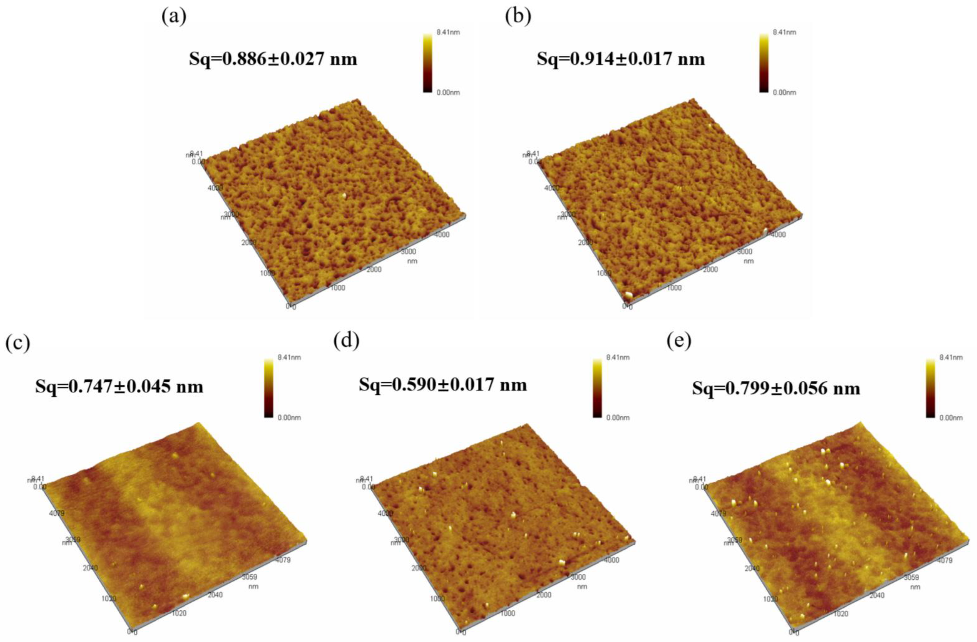
Surface morphology of the thin films was scanned using AFM, as show in Figure 6, and surface roughness was calculated, as shown in Figure 7. The roughness of all five samples of dielectric films is less than 1 nm, indicating good uniformity of the dielectric films prepared by the solution method, providing potential for the fabrication of high-performance devices.
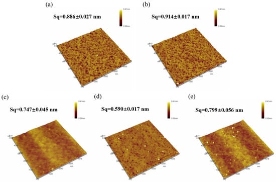
Figure 6.
AFM morphology of Al2O3 films: (a) S1; (b) S2; (c) S3; (d) S4; (e) S5.
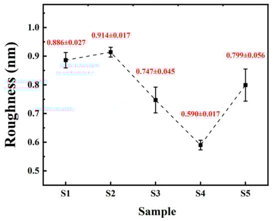
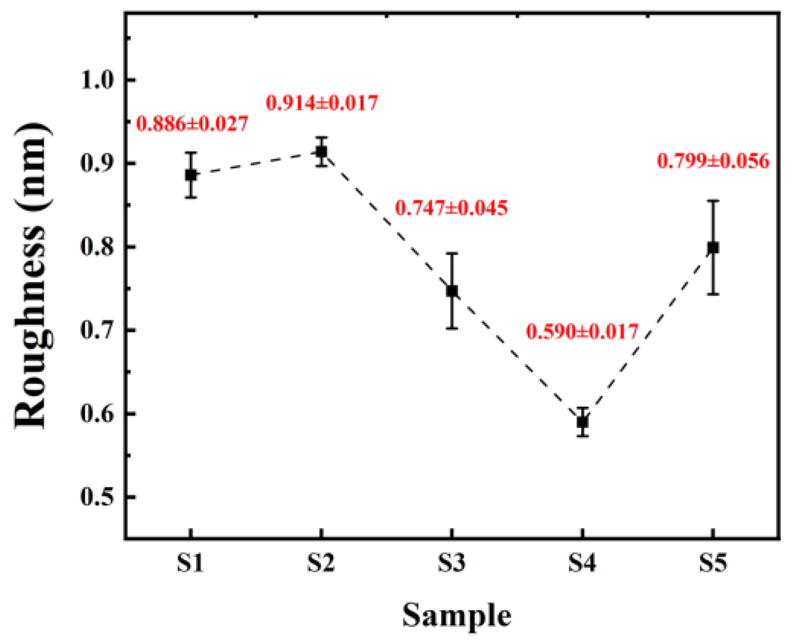
Figure 7.
Surface roughness of different samples.
From Figure 6, it can be observed that both samples of non-self-exothermic system dielectric film surfaces exhibit relatively high roughness and numerous surface pores. This is due to the insufficient annealing temperature, resulting in a lower degree of film densification and, thus, the formation of more pores. In contrast, the surface roughness of the dielectric films in the three self-exothermic system samples is lower than that of the non-self-exothermic system samples. This indicates that the significant heat generated during annealing in the self-exothermic system contributes to an increased level of film densification. The surface roughness of samples S3 and S5 reached 0.747 ± 0.045 nm and 0.799 ± 0.056 nm, respectively. Meanwhile, the surface roughness of sample of S4 reached the lowest at 0.590 ± 0.017 nm, demonstrating the best performance. From Figure 6e, it can also be observed that there is a significant amount of particle precipitation on the surface of the S5 dielectric film. This is consistent with the results of LSCM testing, indicating that a higher content of AlAC leads to easier precipitation during annealing.
3.4. Thin Film Thickness Measurement
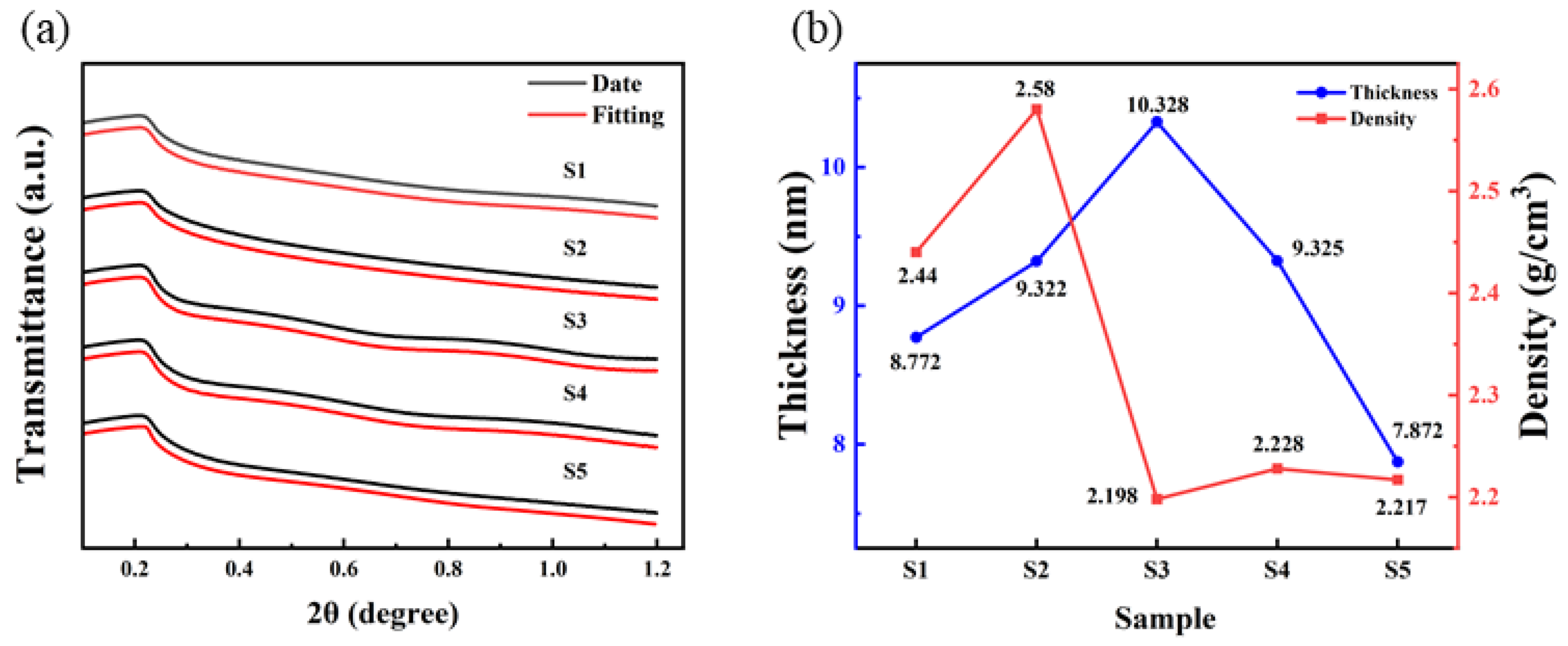
The insulation performance is closely related to the thickness, roughness, and density of the dielectric films [33]. XRR was used to fit the thickness and density, as shown in Figure 8. It is found that the thickness of samples of S1, S2, S3, S4 and S5 is 8.772 nm, 9.322 nm, 10.328 nm, 9.325 nm, and 7.872 nm.
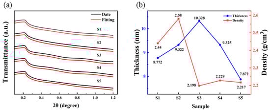
Figure 8.
Al2O3 films: (a) XRR date and fitting curves; (b) thickness and density fitting results.
3.5. Transmittance Test
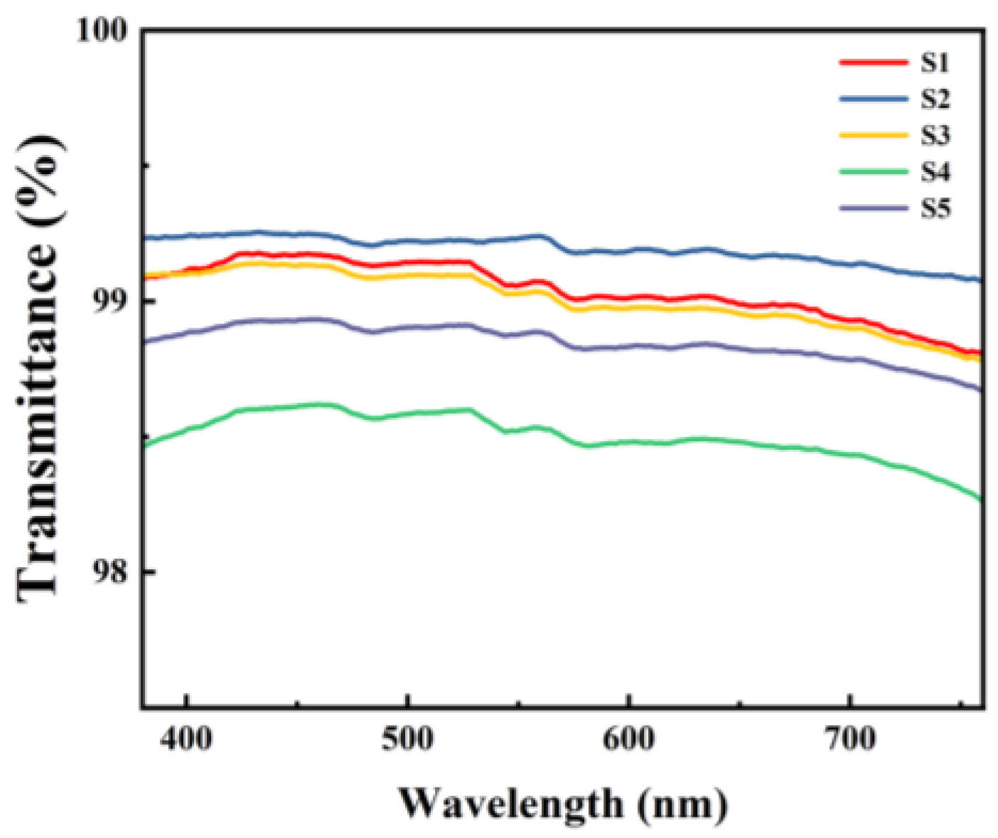
The transmittance of the dielectric films was measured using UV-vis, and the test results are shown in Figure 9. Within the visible light range (400–760 nm), all five samples of films exhibited transmittance rates of over 98%, demonstrating excellent optical performance.
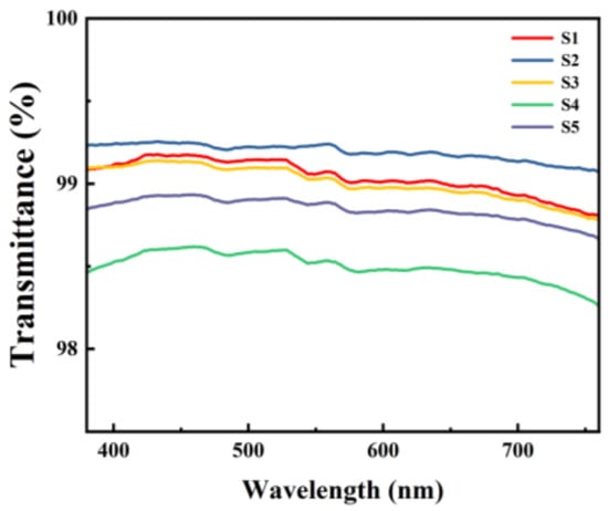
Figure 9.
UV-Vis spectrum of different Al2O3 films.
3.6. Leakage Current Density Analysis
Figure 10 displays the I–V testing curves of five sets of dielectric thin films. Within the tested range, the leakage current density of S3 and S4 is lower than that of S1 and S2, with S3 exhibiting the lowest leakage current density in the 0 to 5 MV/cm range. This indicates that a self-exothermic reaction contributes to the formation of M-O-M bonds within the film and the reduction in defect state density. Conversely, at higher electric fields, the leakage current density of S5 approaches that of S1 and S2, which may be attributed to the higher surface roughness of the S5 film, leading to increased defects in the contact area between the electrode and the film, thereby increasing the leakage current. Furthermore, the zero points of the IV curves for S3 are primarily located around 0 MV/cm, whereas the zero points for S1, S2, and S4 are shifted to around −2 to −1 MV/cm. This also indicates that a self-exothermic reaction helps to reduce internal defects within the film, thereby suppressing zero-point drift.
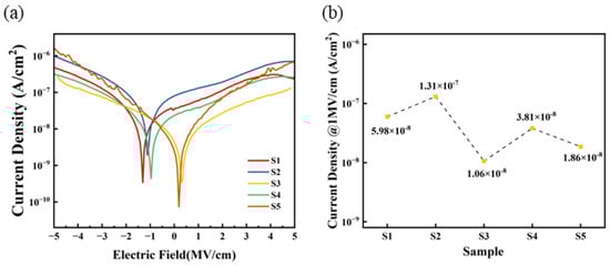
Figure 10.
Al2O3 dielectric films: (a) leakage current density curves; (b) summary of leakage current density @1 MV/cm.
When an electric field of 1 MV/cm is applied, the leakage current densities of the three exothermic system (S3, S4, and S5) devices are 1.06 × 10⁻⁸ A/cm2, 3.81 × 10⁻⁸ A/cm2, and 1.86 × 10⁻⁸ A/cm2, respectively.
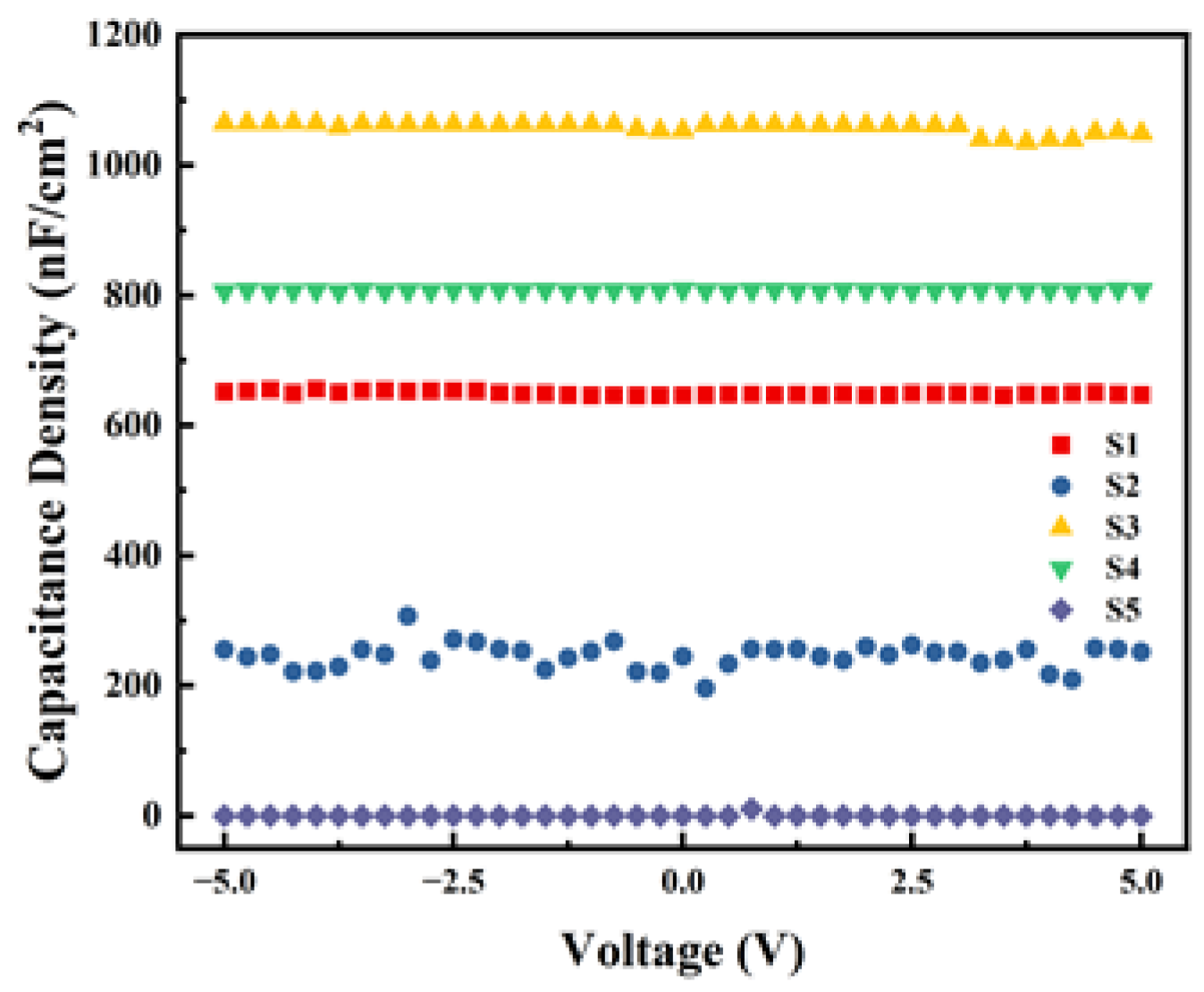
3.7. Capacitance Density Analysis
Capacitance density (Ci) is one of the important parameters of the dielectric layer, reflecting the capacity of storing electrical charge per unit area of the film. The results of the C-V tests are shown in Figure 11. From the results, within the test range, S3 and S4 exhibit good capacitance–voltage stability and higher Ci. However, the Ci of the two non-exothermic system devices is smaller, indicating that the significant heat released by the exothermic process benefits the formation of M-O-M bonds within the dielectric film. During the experiment, the Ci of S5 was so low that it exceeded the instrument’s range, resulting in a value close to zero. Combined with the unstable Ci observed in S2 and the results of surface roughness tests, we can conclude that even with exothermic reactions occurring, the excessive surface roughness of the film significantly affects the performance and stability of the devices.

Figure 11.
Capacitance density test curves of different samples.
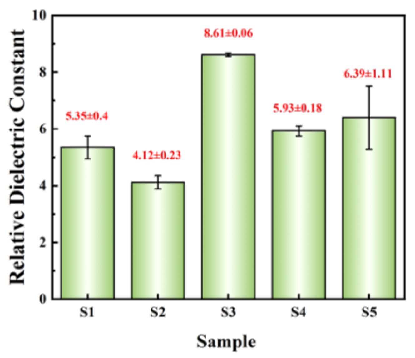
The relative dielectric constant of dielectric films is further investigated. C-F tests were conducted on MIM devices. The relative dielectric constant can be calculated based on the C-F test results and the thickness of dielectric films, which can be calculated as follows:
where ε0 is the vacuum permittivity (8.85 × 10⁻¹² F/m), d represents the thickness of films, and s denotes the area of Al electrode (1.256 × 10⁻³ cm2). The relative dielectric constants @ 1 kHz of dielectric films are summarized in Figure 12. The relative dielectric constants of the three exothermic system films are all greater than those of the other two non-exothermic system films, which once again demonstrates the promoting effect of exothermic reactions. S3 exhibits the highest relative dielectric constant (8.61 ± 0.06) and the smallest standard deviation, indicating excellent dielectric performance and uniformity of the film.
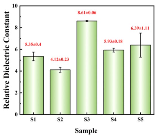
Figure 12.
Summary of relative dielectric constant @1 kHz.
Finally, I have listed a comparison of the key performance characteristics between the films discussed in this article and those produced using the most advanced methods currently available in Table 2. From the table, the Al2O3 films in this study exhibit superior performance in terms of leakage current density and dielectric constant compared to those prepared using auxiliary equipment. At the same time, the Al2O3 films in this article show performance in leakage current density that is comparable to films prepared via vacuum deposition methods and even surpasses the performance of some individual films. Therefore, the low-temperature self-exothermic reaction method for preparing dielectric films based on solution processing presented in this article is not only easy to operate and requires simple equipment but also demonstrates excellent performance, showing great potential. However, this method still faces several issues and challenges. Firstly, since the method is based on solution processing, the evaporation of the solvent during the annealing process can result in the formation of numerous pores of varying sizes within the film. This may lead to reduced film density and adhesion to substrates and increase leakage current density. Secondly, the organic solvents used in this study cause the formation of more pores on the film’s surface during annealing, which increases the surface roughness and thus affects the electrical properties of the film.
Table 2.
A thorough quantitative comparison of leakage current density and dielectric constant against state-of-the-art methods.
4. Conclusions
This paper employs a low-temperature self-exothermic reaction based on the solution method to fabricate high-performance transparent Al2O3 dielectric films at an annealing temperature of 185 °C. The experiments demonstrate that mixed systems of AlNO and AlAC in varying proportions undergo vigorous redox reactions and release significant heat at around 160~180 °C. During the annealing process, a higher content of AlAC results in more pronounced surface precipitation and higher surface roughness of the film. Therefore, based on comprehensive analysis, S3 exhibits the best performance: the AFM test results indicate a surface roughness of 0.747 ± 0.045 nm; the transmittance within the visible light range reaches up to 98%; the device leakage current density is as low as 1.06 × 10⁻⁸ A/cm2@1 MV/cm, with a high relative dielectric constant of 8.61 ± 0.06, demonstrating excellent electrical characteristics and stability. In summary, the alumina films prepared using the exothermic solution method reported in this paper exhibit lower annealing temperatures and surface roughness, higher transparency, lower leakage current density, and higher relative dielectric constant. These characteristics offer great promise for compatibility with flexible substrates and the fabrication of high-performance transparent electronic devices.
Author Contributions
Writing—original draft preparation, X.F.; writing—review and editing, R.Y. and H.N.; methodology, Z.Z.; conceptualization, H.N.; investigation, W.C. and S.J.; validation, J.P. and Y.H.; formal analysis, Y.Y.; supervision, D.L. All authors have read and agreed to the published version of the manuscript.
Funding
This work was supported by the National Key R&D Program of China (No. 2021YFB3600604), the National Natural Science Foundation of China (Grant No. 62174057, 62375057, 62074060 and 22090024), the Guangdong Natural Science Foundation (No. 2024A1515012216 and 2023A1515011026), the Educational Commission of Guangdong Province (Grant Nos. 2022ZDZX1002), and the Key R&D Plan of Guangdong Province (2022B0303010001), State Key Lab of Luminescent Materials and Devices (Skllmd-2024-05), Southwest Institute of Technology and Engineering Cooperation Fund (HDHDW59A020301), the open research fund od Songshan Lake Materials Laboratory (2022SLABFN05), Science and Technology Program of Guangdong (Grant No. 2024A0505040026), Guangdong Basic and Applied Basic Research Foundation (Grant No. 2022A1515140064, 2023B1515120046 and 2024A1515012019), Science and Technology Program of Guangzhou (Grant No. 2023A03J0024), Research Project of Guangzhou University (Grant No. ZH2023006), the Guangdong Provincial Key Laboratory of Optical Information Materials and Technology (2023B1212060065), and the Key Laboratory of Optoelectronic Devices and Systems of Ministry of Education and Guangdong Province.
Data Availability Statement
The data are contained within the article.
Acknowledgments
We thank all the participants, institutions, editors, and reviewers for enabling us to conduct this research.
Conflicts of Interest
The authors declare no conflicts of interest.
References
- Yi, Z.; Lyu, B.; Gao, D.; Hao, J.; Liu, Z.; Ning, Z.; Jiang, B. Preparation Strategy and Composition Design of Polymer-Based Layered Composites for Improving Energy Storage Performances. J. Energy Storage 2024, 92, 111995. [Google Scholar] [CrossRef]
- Huan, T.D.; Boggs, S.; Teyssedre, G.; Laurent, C.; Cakmak, M.; Kumar, S.; Ramprasad, R. Advanced Polymeric Dielectrics for High Energy Density Applications. Prog. Mater. Sci. 2016, 83, 236–269. [Google Scholar] [CrossRef]
- Yao, Z.; Song, Z.; Hao, H.; Yu, Z.; Cao, M.; Zhang, S.; Lanagan, M.T.; Liu, H. Homogeneous/Inhomogeneous-Structured Dielectrics and Their Energy-Storage Performances. Adv. Mater. 2017, 29, 1601727. [Google Scholar] [CrossRef] [PubMed]
- Mukherjee, A.; Nagaria, R.K. A Comparative Study of Various High-K Dielectric Materials as Gate Oxide Layer on TG FinFET. In Proceedings of the 2021 2nd Global Conference for Advancement in Technology (GCAT), Bangkok, Thailand, 1–3 October 2021; pp. 1–4. [Google Scholar] [CrossRef]
- Han, D.; Geng, Y.; Cai, J.; Wang, W.; Wang, L.; Tian, Y.; Wang, Y.; Liu, L.; Zhang, S. Reliability Study of Zinc Oxide Thin-Film Transistor with High-K Gate Dielectric. In Proceedings of the 2012 IEEE International Conference on Electron Devices and Solid State Circuit (EDSSC), Bangkok, Thailand, 3–5 December 2012; pp. 1–2. [Google Scholar] [CrossRef]
- Gao, H.-X.; Hu, R.; Yang, Y.-T. The Theoretical Investigation and Analysis of High-Performance ZnO Double-Gate Double-Layer Insulator Thin-Film Transistors. Chin. Phys. Lett. 2012, 29, 017305. [Google Scholar] [CrossRef]
- Xie, J.; Zhu, Z.; Tao, H.; Zhou, S.; Liang, Z.; Li, Z.; Yao, R.; Wang, Y.; Ning, H.; Peng, J. Research Progress of High Dielectric Constant Zirconia-Based Materials for Gate Dielectric Application. Coatings 2020, 10, 698. [Google Scholar] [CrossRef]
- Robertson, J. High Dielectric Constant Oxides. Eur. Phys. J. Appl. Phys 2004, 28, 265–291. [Google Scholar] [CrossRef]
- Wang, Y.; Han, T.; Yang, L.; Wang, B.; Xue, J.; Yi, S.; Xie, A.; Cao, C. A Novel IGZO-TFT Device With High Dielectric Constant Sandwich Structure Gate Dielectric Layer. In Proceedings of the 2023 24th International Conference on Electronic Packaging Technology (ICEPT), Shihezi City, China, 8–11 August 2023; pp. 1–5. [Google Scholar] [CrossRef]
- Shrivastava, S.; Bahubalindruni, P.G.; Goes, J. A Pulse Width Modulator Using a High-Speed Comparator With Flexible Oxide TFT Technology. IEEE Solid-State Circuits Lett. 2022, 5, 288–291. [Google Scholar] [CrossRef]
- Deng, X.; Zhang, Y.; Fu, H.; Zhang, S. High Mobility Metal-Oxide Thin Film Transistors with IGZO/In2O3 Dual-Channel Structure. In Proceedings of the 2018 9th Inthernational Conference on Computer Aided Design for Thin-Film Transistors (CAD-TFT), Shenzhen, China, 16–18 November 2018; pp. 1–3. [Google Scholar] [CrossRef]
- Yang, Z.; Pu, H.; Cui, C.; Zhang, L.; Dong, C.; Zhang, Q. Solution-Processed Indium–Zinc-Oxide Thin Film Transistors With High- k Magnesium Titanium Oxide Dielectric. IEEE Electron. Device Lett. 2014, 35, 557–559. [Google Scholar] [CrossRef]
- Wang, B.; Huang, W.; Chi, L.; Al-Hashimi, M.; Marks, T.J.; Facchetti, A. High-k Gate Dielectrics for Emerging Flexible and Stretchable Electronics. Chem. Rev. 2018, 118, 5690–5754. [Google Scholar] [CrossRef]
- Devaray, P.; Hatta, S.F.W.M.; Wong, Y.H. An Overview of Conventional and New Advancements in High Kappa Thin Film Deposition Techniques in Metal Oxide Semiconductor Devices. J. Mater. Sci. Mater. Electron. 2022, 33, 7313–7348. [Google Scholar] [CrossRef]
- Johnson, R.W.; Hultqvist, A.; Bent, S.F. A Brief Review of Atomic Layer Deposition: From Fundamentals to Applications. Mater. Today 2014, 17, 236–246. [Google Scholar] [CrossRef]
- Christen, H.M.; Eres, G. Recent Advances in Pulsed-Laser Deposition of Complex Oxides. J. Phys. Condens. Matter 2008, 20, 264005. [Google Scholar] [CrossRef]
- Joung, S.-Y.; Yim, H.; Lee, D.; Shim, J.; Yoo, S.Y.; Kim, Y.H.; Kim, J.S.; Kim, H.; Hyeong, S.-K.; Kim, J.; et al. All-Solution-Processed High-Performance MoS2 Thin-Film Transistors with a Quasi-2D Perovskite Oxide Dielectric. ACS Nano 2024, 18, 1958–1968. [Google Scholar] [CrossRef] [PubMed]
- Jaehnike, F.; Pham, D.V.; Anselmann, R.; Bock, C.; Kunze, U. High-Quality Solution-Processed Silicon Oxide Gate Dielectric Applied on Indium Oxide Based Thin-Film Transistors. ACS Appl. Mater. Interfaces 2015, 7, 14011–14017. [Google Scholar] [CrossRef] [PubMed]
- Ji, S.-B.; Seong, N.; Park, J.; Im, H.; Kim, Y.-S.; Hong, Y. Field-Effect Mobility Extraction of Solution-Processed InGaZnO Thin-Film Transistors Considering Dielectric Dispersion Behavior of AlOx Gate Insulator. ACS Appl. Electron. Mater. 2023, 5, 1035–1040. [Google Scholar] [CrossRef]
- He, W.; Wang, S.; Hang, B.; Wei, X.; Liang, L. Development of Solution-Processed Organic Semiconductor Thin Films. In Interdisciplinary Research for Printing and Packaging; Zhao, P., Ye, Z., Xu, M., Yang, L., Zhang, L., Yan, S., Eds.; Springer Singapore: Singapore, 2022; pp. 471–479. [Google Scholar] [CrossRef]
- Liu, Q.; Zhao, C.; Zhao, T.; Liu, Y.; Mitrovic, I.Z.; Xu, W.; Yang, L.; Zhao, C.Z. Ecofriendly Solution-Combustion-Processed Thin-Film Transistors for Synaptic Emulation and Neuromorphic Computing. ACS Appl. Mater. Interfaces 2021, 13, 18961–18973. [Google Scholar] [CrossRef]
- Quah, H.J.; Cheong, K.Y.; Hassan, Z.; Lockman, Z.; Jasni, F.A.; Lim, W.F. Effects of Postdeposition Annealing in Argon Ambient on Metallorganic Decomposed CeO2 Gate Spin Coated on Silicon. J. Electrochem. Soc. 2009, 157, H6. [Google Scholar] [CrossRef]
- Xu, W.; Long, M.; Zhang, T.; Liang, L.; Cao, H.; Zhu, D.; Xu, J.-B. Fully Solution-Processed Metal Oxide Thin-Film Transistors via a Low-Temperature Aqueous Route. Ceram. Int. 2017, 43, 6130–6137. [Google Scholar] [CrossRef]
- Jo, J.-W.; Kim, K.-H.; Kim, J.; Ban, S.G.; Kim, Y.-H.; Park, S.K. High-Mobility and Hysteresis-Free Flexible Oxide Thin-Film Transistors and Circuits by Using Bilayer Sol–Gel Gate Dielectrics. ACS Appl. Mater. Interfaces 2018, 10, 2679–2687. [Google Scholar] [CrossRef]
- Wang, S.; Yao, S.; Lin, J.; Xia, G. Eco-Friendly, Low-Temperature Solution Production of Oxide Thin Films for High-Performance Transistors via Infrared Irradiation of Chloride Precursors. Ceram. Int. 2019, 45, 9829–9834. [Google Scholar] [CrossRef]
- Arias, A.C.; MacKenzie, J.D.; McCulloch, I.; Rivnay, J.; Salleo, A. Materials and Applications for Large Area Electronics: Solution-Based Approaches. Chem. Rev. 2010, 110, 3–24. [Google Scholar] [CrossRef] [PubMed]
- Jung, Y.; Jun, T.; Kim, A.; Song, K.; Yeo, T.H.; Moon, J. Direct Photopatternable Organic–Inorganic Hybrid Gate Dielectric for Solution-Processed Flexible ZnO Thin Film Transistors. J. Mater. Chem. 2011, 21, 11879–11885. [Google Scholar] [CrossRef]
- Hwang, J.; Lee, J.; Kim, Y.; Lee, E.; Wang, Y.; Kim, H. Hybrid Gate Insulator for OTFT Using Dip-Coating Method. Curr. Appl. Phys. 2011, 11, S154–S157. [Google Scholar] [CrossRef]
- Wong, H.-S.P.; Lee, H.-Y.; Yu, S.; Chen, Y.-S.; Wu, Y.; Chen, P.-S.; Lee, B.; Chen, F.T.; Tsai, M.-J. Metal-Oxide RRAM. Proc. IEEE 2012, 100, 1951–1970. [Google Scholar] [CrossRef]
- El-Shereafy, E.; Abousekkina, M.M.; Mashaly, A.; El-Ashry, M. Mechanism of Thermal Decomposition and γ-Pyrolysis of Aluminum Nitrate Nonahydrate [Al(NO3)3·9H2O]. J. Radioanal. Nucl. Chem. 1998, 237, 183–186. [Google Scholar] [CrossRef]
- Melnikov, P.; Nascimento, V.A.; Arkhangelsky, I.V.; Zanoni Consolo, L.Z. Thermal Decomposition Mechanism of Aluminum Nitrate Octahydrate and Characterization of Intermediate Products by the Technique of Computerized Modeling. J. Therm. Anal. Calorim. 2013, 111, 543–548. [Google Scholar] [CrossRef]
- Mandai, T.; Johansson, P. Haloaluminate-Free Cationic Aluminum Complexes: Structural Characterization and Physicochemical Properties. J. Phys. Chem. C 2016, 120, 21285–21292. [Google Scholar] [CrossRef]
- Jung, S.H.; Han, H.S.; Kim, Y.B.; Kim, D.S.; Deshpande, N.G.; Oh, S.J.; Choi, J.H.; Cho, H.K. Toward Ultraviolet Solution Processed ZrOx/IZO Transistors with Top-Gate and Dual-Gate Operation: Selection of Solvents, Precursors, Stabilizers, and Additive Elements. J. Alloys Compd. 2020, 847, 156431. [Google Scholar] [CrossRef]
- Padhi, P.S.; Ajimsha, R.S.; Chetia, S.K.; Das, A.K.; Sahu, V.K.; Misra, P. Reduced Leakage Current in Al2O3/TiO2/Al2O3 Dielectric Stacks Grown by Pulsed Laser Deposition. AIP Conf. Proc. 2020, 2265, 030190. [Google Scholar] [CrossRef]
- Kwak, H.Y.; Kwon, H.M.; Kwon, S.K.; Jang, J.H.; Sung, S.Y.; Lim, S.; Lee, H.D. Dielectric Relaxation and Reliability of Al2O3-HfO2-Al2O3 Sandwiched Metal-Insulator-Metal (MIM) Capacitor. AMR 2013, 658, 116–119. [Google Scholar] [CrossRef]
- Choi, C.H.; Kim, T.; Ueda, S.; Shiah, Y.-S.; Hosono, H.; Kim, J.; Jeong, J.K. High-Performance Indium Gallium Tin Oxide Transistors with an Al2O3 Gate Insulator Deposited by Atomic Layer Deposition at a Low Temperature of 150 °C: Roles of Hydrogen and Excess Oxygen in the Al2O3 Dielectric Film. ACS Appl. Mater. Interfaces 2021, 13, 28451–28461. [Google Scholar] [CrossRef] [PubMed]

Disclaimer/Publisher’s Note: The statements, opinions and data contained in all publications are solely those of the individual author(s) and contributor(s) and not of MDPI and/or the editor(s). MDPI and/or the editor(s) disclaim responsibility for any injury to people or property resulting from any ideas, methods, instructions or products referred to in the content. |
© 2024 by the authors. Licensee MDPI, Basel, Switzerland. This article is an open access article distributed under the terms and conditions of the Creative Commons Attribution (CC BY) license (https://creativecommons.org/licenses/by/4.0/).