Article

Growth of Ultra-Long ZnO Microtubes Using a Modified Vapor-Solid Setup

Department of Mechanical and Aerospace Engineering, University of Texas, Arlington, TX 76019, USA
*
Author to whom correspondence should be addressed.
Micromachines 2014, 5(4), 1069-1081; https://doi.org/10.3390/mi5041069
Submission received: 27 August 2014 / Revised: 4 November 2014 / Accepted: 6 November 2014 / Published: 11 November 2014
(This article belongs to the Special Issue Micro/Nano Fabrication)

Abstract

:
In this work, we have modified the experimental setup for a vapor-solid (VS) process to synthesize Zinc oxide (ZnO) microtubes (MTs) with lengths up to 3 mm during a 90-min growth period. The critical idea behind this modification is to control the distribution of Zn vapor along the Si substrates. The morphology evolution of ZnO structures with the increasing reaction time was particularly explored. We found that, within the 90-min growth period, four different types of ZnO microstructures appeared in this synthesis process: microrods (MRs), short MTs, two-tier structures, and long MTs. Growth mechanisms were proposed to interpret the formation of these structures.

1. Introduction

Zinc oxide (ZnO), one of the most important functional materials, has attracted wide attention because of its unique semiconducting, piezoelectric, and optoelectronic properties, which have promising applications in electronics [1], optoelectronics [2], photodetectors [3,4], power generators [5] and microfluidic devices [6], to name a few. In the past few decades, substantial effort has been devoted to the optimization of its chemical composition [7,8,9], morphology [1,10,11,12,13], and crystal size [14,15]. Meanwhile, various synthetic methodologies have been explored to make new structures [16]. The commonly applied methods to grow 1-D ZnO micro/nanostructures mainly include vapor [17,18,19] and solution-phase approaches [20,21,22,23]. Solution-phase methods have been widely proposed and employed to construct precise morphology due to their low growth temperatures and good potential for scale-up. However, due to their low growth rates (because of low synthesis temperatures), long ZnO microstructures are difficult to achieve using these approaches [23,24,25]. On the other hand, in contrast to nanostructures, long microstructures are relatively easy to manipulate under an optical microscope and integrate into functional circuits. High processing temperatures are adopted in vapor-phase approaches, enabling these approaches to have high growth rates. Accordingly, the vapor-phase approaches are often applied to grow long ZnO microstructures, which are also employed in this work.
As members in the family of 1-D ZnO structures, wires and tubes have recently received much attention due to their unique structures and potential applications in the fields of piezoelectric generators, solar cells, surface modification, fog collection, and so on [24,25,26,27,28,29,30,31,32]. To the best of our knowledge, until now, a challenge still exists in the rational design and facile synthesis of long ZnO microtubes (MTs), although ZnO nanotubes [33,34,35,36,37] have been extensively studied in recent years. Aqueous solution routes [38,39] were used for fabricating ZnO MTs with poly-crystalline structures. In order to improve the crystal quality, microwave-heating method [40] has been applied to synthesize single-crystalline ZnO MTs, whose lengths and diameters are 250 and 80 μm, respectively. In addition, ZnO MTs have also been grown in molten alkali metal salt [41]. The as-prepared MTs were up to 250 μm in length with high polydispersity. However, this method involves impurity ions, and the properties of the product may be affected by the unintentional contamination. To circumvent the limitations of the existing methods in synthesizing long ZnO MTs, we have developed a modified vapor-phase setup in this work.

2. Experimental Setups
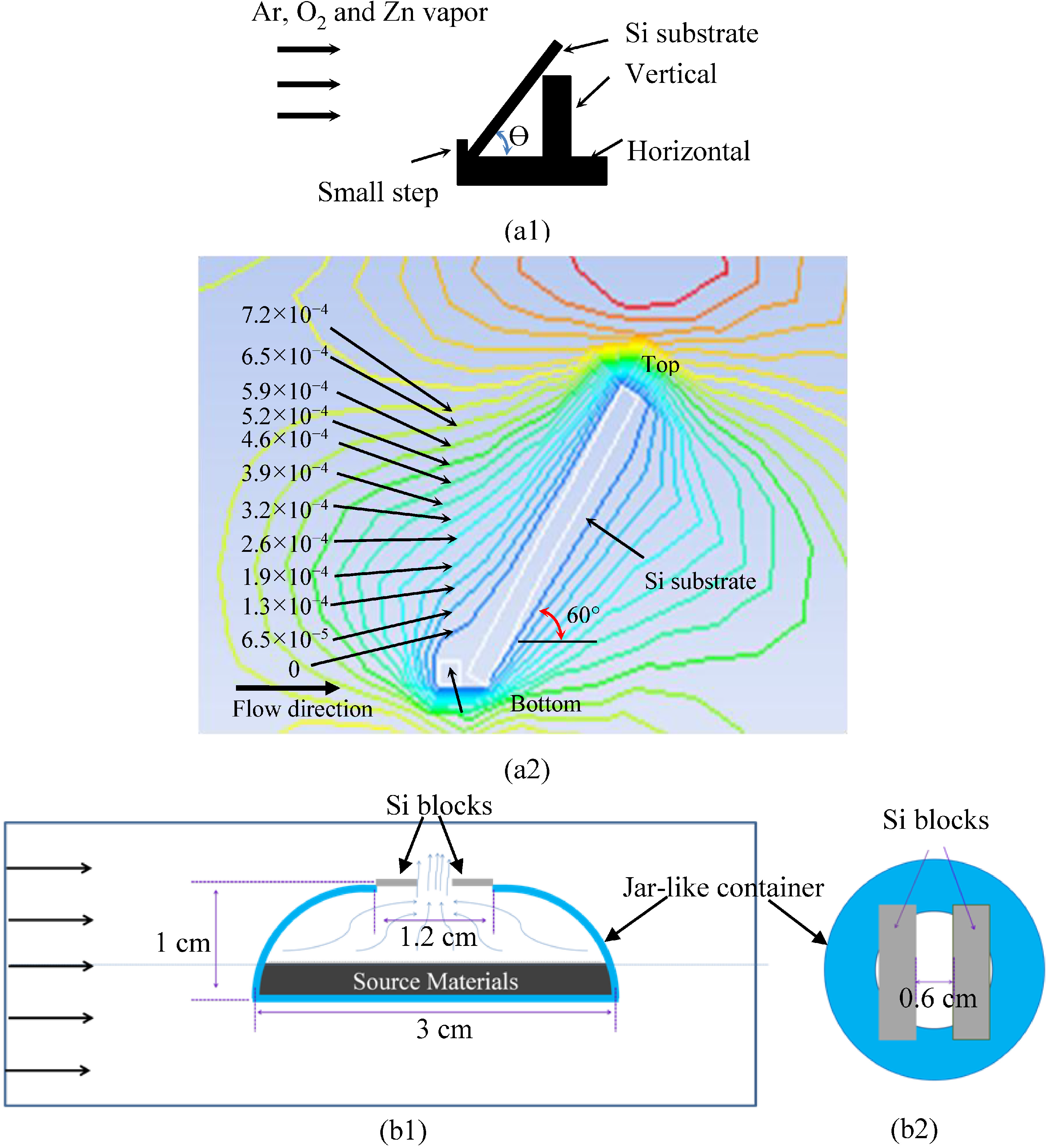
2.1. Previous Setup

Figure 1(a1) shows part of a setup that we have previously used to grow ZnO wires [42]. It includes a horizontal tube furnace, a graphite crucible, and a quartz boat. ZnO and graphite powders are mixed in the graphite crucible, which is subsequently placed in the center of the furnace. A Si substrate is put on the quartz boat. The quartz boat consists of a horizontal plate and a movable vertical support. The horizontal plate has a small step on its front side. The substrate is put between this step and the vertical support (Figure 1(a1)). By moving the vertical support forward or backward along the horizontal plate, the substrate can be tilted at different angles. Consequently, the orientation of this substrate can be adjusted between 0° and 90° relative to the incoming gas flow. Other researchers usually set the tilt angle to be 0° when growing ZnO structures [43,44]. However, we varied the tilt angle to examine its effect on synthesized products [42]. The quartz boat is positioned in the middle of the furnace. Afterwards, the tube in the furnace is heated up from room temperature to 950 °C. Subsequently, Ar and O2 gases are introduced into the reactor. Meanwhile, Zn vapor is continuously generated by carbothermal reduction of ZnO powder in the graphite crucible, following the chemical reaction: C(s) + ZnO(s) → CO(g) + Zn(g). The produced Zn vapor is brought over by the incoming gas flow to the Si substrate, and has reaction with O2 over there to produce ZnO wires. After the high temperature is maintained for 90 min, Ar and O2 systems are switched off and the furnace is cooled naturally to room temperature.
In the previous work [42], we also simulated the flow patterns over the Si substrate when its tilt angle varied from 0° to 80° with an increment of about 15°. We found: (i) the tilt angles affect the corresponding flow patterns, resulting in ZnO wires with different lengths and densities, and (ii) the incoming flow hits the small step located on the front edge of the horizontal plate, jumps up and subsequently flows down towards the Si substrate (Figure 1(a2)).
Figure 1. (a1) Side view of part of a setup previously employed to synthesize ZnO wires, and (a2) flow patterns around the Si substrate for 60° tilt angle; (b1) Side view of the new setup used in this work to grow Zinc oxide (ZnO) microtubes (MTs), and (b2) top view of the jar-like container, on which two Si blocks are placed as product collectors.
Micromachines 05 01069 g001
Under steady-state conditions of gas flows, the concentration of a reactant on the surface, ns, is determined by several factors as given below [45,46]:
n s = n g 1 + k s δ D
where ng is the concentration of reactant in the gas flow, ks is the surface reaction constant, δ is the thickness of a boundary layer on the substrate, and D is the gas phase diffusivity constant. The boundary layer encloses a relatively stagnant layer through which the gaseous reactants have to diffuse in order to reach the surface of the substrate to form the nanowires. Outside this layer the fluid flows with a constant bulk speed, as if there is no friction. δ was considered to be the distance between the substrate and the point with speed 0.99U, where U was the bulk speed.
By Equation (1), when other factors are fixed, ns decreases with δ. As δ approaches zero, ns equals ng, and the growth process is dominated by the concentration of reactants in the incoming gas flow. When δ is very large, ns approaches zero and the growth of the nanowires is limited by the transport of reactants across the boundary layer. Therefore, according to flow pattern illustrated in Figure 1(a2), the concentrations of both gases are higher on the top surfaces of formed ZnO structures than on the sidewalls of these structures during the process of generating these structures, and the concentrations of these gases are lower at a location close to the small step than at a place far away from this step. Thus, ZnO wires were generated on the substrate, and their lengths and densities increase with the increase in the distance between the small step and the growth spots. For example, when the substrate was tilted at an angle of 60°, the density and length increased from 0.1 × 10⁷ wires/cm2 and 0.5 μm at a location beside the small step to 5.4 × 10⁷ wires/cm2 and 12 μm at the other end of this 16-mm-long substrate. These results clearly indicate that geometric dimensions of grown ZnO products are affected by the surrounding flow pattern. Motivated by this point, in this work, we originally desired to modify the flow pattern through a new setup. We expected to grow long ZnO wires through this new setup. However, to our surprise, long ZnO MTs were synthesized instead, as will be addressed in detail in Section 3.

2.2. Modified Setup

The modified setup used in this work is shown in Figure 1b. It includes a horizontal tube furnace and a jar-like quartz container (A.M. Quartz Co., Grainesville, FL, USA). The tube is 55 cm long and has a diameter of 4.4 cm. The jar-like quartz container is about 1 cm tall. The diameters of its bottom surface and top opening are 3 and 1.2 cm, respectively. ZnO powder (Fisher Scientific Co., Pittsburgh, PA, USA) and graphite powder (Sigma-Aldrich Co., St. Louis, MO, USA) with equal weight (0.5 g) are mixed and put into this container. Two identical Si blocks are placed on the opening of the container in a parallel manner, serving as substrates for growing ZnO MTs. The distance between the two blocks is 6 mm. Each block is 3 cm long, 5 mm wide and 500 μm thick. These blocks are cut out of a 4-inch Si wafer using a dicing saw (model: Disco AD3220, Disco Co., Tokyo, Japan). After being loaded with source materials and Si blocks, the container is placed in the center of the furnace. During a growth process, the tube in the furnace is heated at a rate of 30 °C/min from room temperature to 950 °C, and this temperature is then fixed for different times to generate different ZnO structures. Before we switch on the tube furnace, 80 standard cubic centimeters per minute (sccm) of Ar and 2 sccm of O2 gases are introduced into the reactor. The flow rate of the mixed gases remains unchanged during the whole process. The jar-like container ensures that the mixed source materials have a large contact surface at the bottom surface for producing enough Zn vapors, and that its narrow outlet increases the speeds of these Zn vapors over the two Si blocks.
The new setup also includes a horizontal tube furnace. On the other hand, it has two critical differences from previous setup. First, ZnO and graphite powders are loaded in a jar-like quartz container, instead of in a quartz boat. Second, two Si substrates are placed on the top of the quartz container (not on a quartz boat). As will be addressed in Section 3, these two differences result in new flow patterns around Si substrates.

3. Results and Discussion

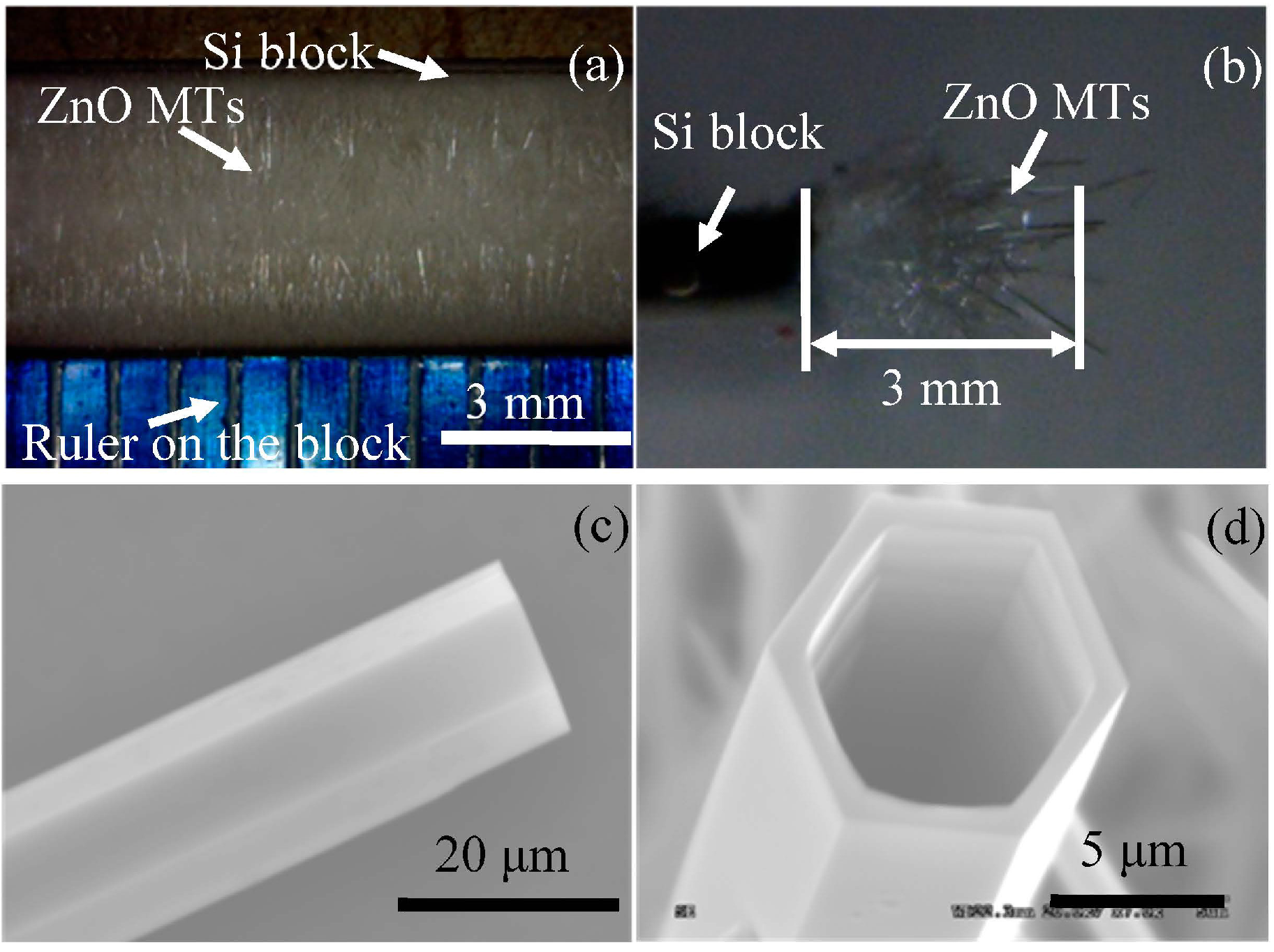
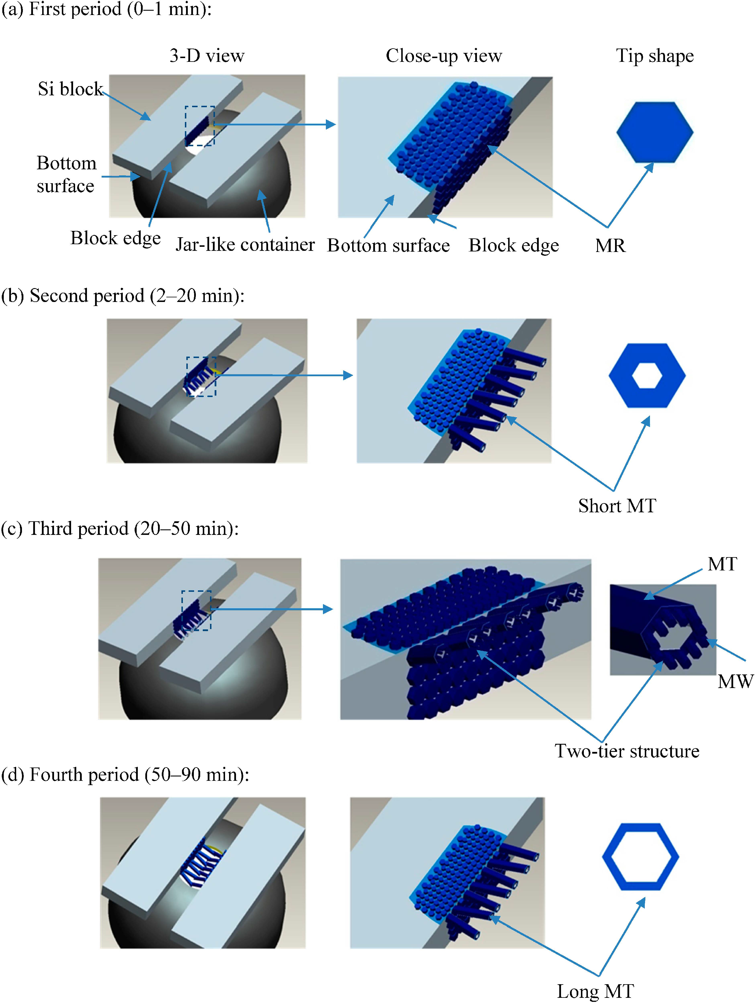
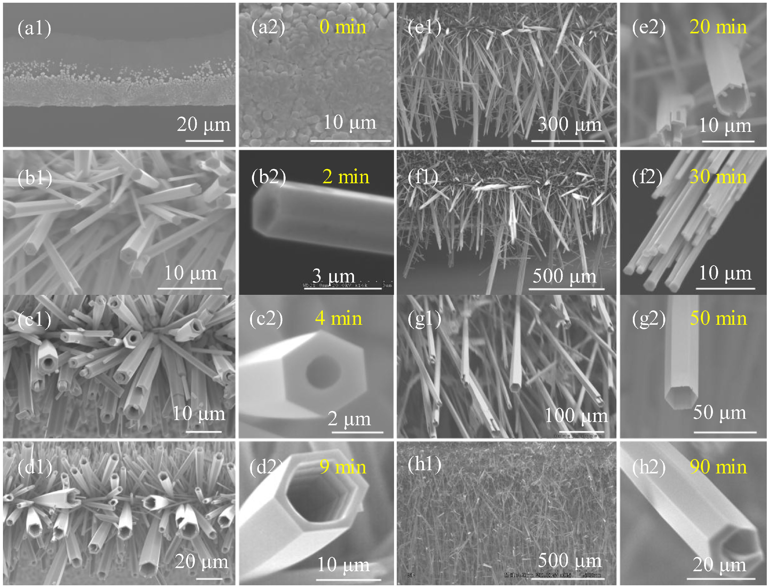
3.1. The Evolution of ZnO Structures

Figure 2 shows ZnO MTs that were grown on the sidewalls of two Si blocks during a 90-min period. ZnO seeds appeared on the Si substrates from around 900 °C. Herein, we considered this point as the starting time in our study. The lengths of these MTs vary from 2.4 to 3 mm, and their outer and inner diameters are about 18 and 9.8 μm, respectively.
Figure 2. (a) Top and (b) side views of ZnO MTs grown on the sidewalls of two Si blocks (optical images). Representative (c) side and (d) top views of ZnO MTs (SEM images).
Micromachines 05 01069 g002
To understand the evolution of ZnO morphology during this 90-min growth period, we prepared eight pairs of identical Si substrates, and ZnO structures were grown on these substrates using the setup shown in Figure 1b for different times. As illustrated in Figure 3 and shown in Figure 4, the generation of MTs with lengths up to 3 mm includes four steps, and different ZnO structures were observed in these steps. At the beginning of the first step (t = 0–2 min), ZnO seeds, which had a form of nanoparticles, were firstly formed on the sidewalls of Si blocks (Figure 3a and Figure 4a). Figure 4a shows a SEM image of the ZnO seed layer on the Si substrate. Since there was a gradient in the concentrations of Zn vapor from one edge to the other, the thickness of the seed layer also has a gradient. As shown in Figure 4(a2), the edge of Si substrate was densely covered by ZnO particles with a mean diameter of ~1 μm. Continuous feeding of Zn vapor into favorable nucleation sites of ZnO seeds causes the continued growth. ZnO microrods (MRs) were subsequently formed on the seeds. Each MR has hexagonal cross-sections, implying that it grew along its c-axis (Figure 4b). The MRs grew up to 10 μm long at the end of the first step, their widths varied from 1 to 3 μm, and the distances between the tips of two neighboring microwires (MWs) were less than 3 μm.
In the second step (t = 2–20 min), short MTs were synthesized on top of short MRs (Figure 3b and Figure 4c–d). At the end of this step, the MT portions have lengths up to ~500 μm; their outer and inner diameters were in the ranges of 8.8–10 μm and 8–8.8 μm, respectively. The distances between the tips of two neighboring MT portions were in the range of 6–75 μm. The distance between the tips of the 1-D structures increased with the growth time, namely, the space between the ZnO microstructures increases as the fan-shaped distribution.
Figure 3. Schematics of synthesized products in the four periods. Many rows of MTs are produced during the growth process, while only a row of them is shown in each set of drawings for illustration purpose. (a) First; (b) second; (c) third; (d) fourth period.
Micromachines 05 01069 g003
In the third step (t = 20–50 min), MWs were formed on top of the short MTs (Figure 3c). Such MWs appeared at the beginning of this step (Figure 4e). They could grow as long as 100 μm and their diameters ranged from 0.5 to 2 μm (Figure 4f). The distances between the tips of two neighboring incomplete MTs were in the range of 75–100 μm. The two-tier structures, which consisted of short MTs and MWs, had total lengths of 500 μm to 1.9 mm.
In the fourth step (t = 50–90 min), long MTs were produced after the MWs were merged as new portions of the MTs [47], and they were also thickened due to continuous generation of ZnO on their sidewalls (Figure 3g–h). At the end of this step, the MTs ranged from 2.4 to 3 mm in their lengths, and their average outer and inner diameters were about 18 and 9.8 μm, respectively. The distances between the tips of two neighboring MTs ranged from 5 to 25 μm.
In this work, we simply focused on the synthesis and geometric structures of the MTs, and did not examine the crystalline structures of these MTs. According to the results of [48], the synthesized MTs may have polycrystalline structures.
Figure 4. ZnO structures generated on sidewalls of Si blocks during four growth periods (SEM images): (a) preformed ZnO seeds; (b) MRs in Step I; (cd) MTs in Step II; (ef) MWs on the wall of MTs in Step III; and (gh) long MTs in Step IV. The corresponding growth times are given in the corresponding images. (a1h1) perspective and (a2h2) close-up views of the ZnO structures.
Micromachines 05 01069 g004

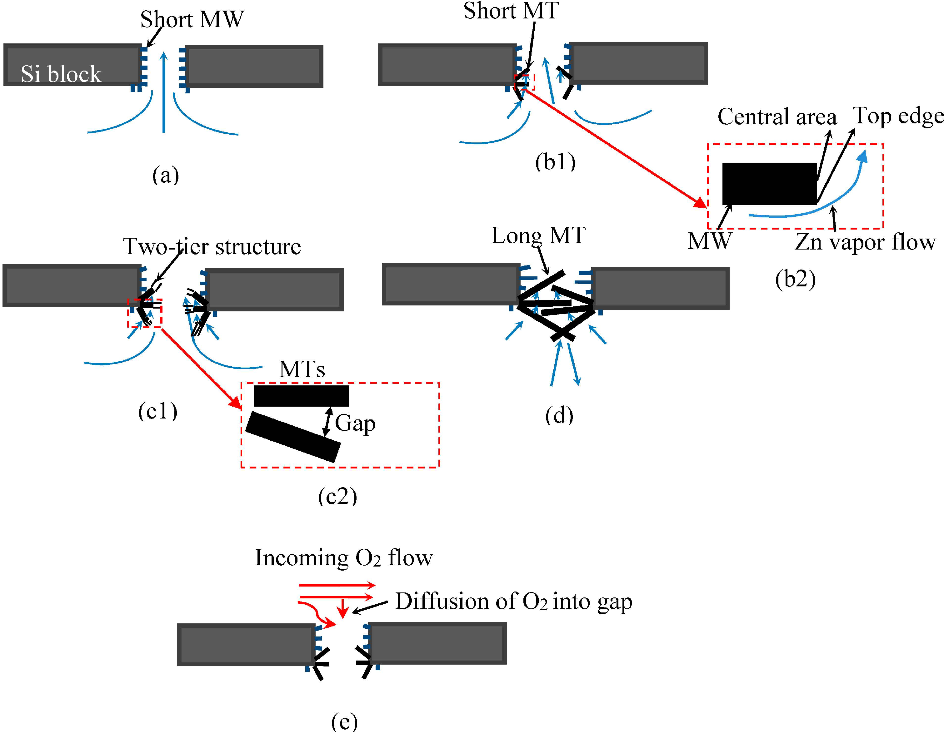
3.2. Growth Mechanism

Mechanisms are proposed to explain the production of the four types of ZnO structures (Figure 5). We consider that these structures are produced mainly due to different Zn vapor concentrations around the tops and sidewalls of ZnO structures in the corresponding growth periods.
As illustrated in Figure 5a, in the first step, Zn vapors were produced on the bottom of the quartz container, went up to its opening, and flowed over the sidewalls of the two Si blocks. Some vapors were absorbed onto the sidewalls. Meanwhile, O2 were transported into the furnace, and spread all over the tube. O2 reacted with Zn vapor at the surfaces and sidewalls of the Si blocks, first producing ZnO seeds and then MRs over there. The temperature in the furnace rose at a rate of 30 °C/min. At the beginning of the formation of Zn vapor, the temperature was below 900 °C. Accordingly, the growth rate was slow because of the low Zn concentration, resulting in the formation of MRs.
In the second step (Figure 5b), the flow patterns around the block sidewalls changed due to the existence of ZnO MRs. The part of Zn vapors which flowed along the sidewall directly penetrated into the gaps between ZnO MRs. However, the other part of Zn vapors that did not flow directly along this sidewall has a flow pattern similar to the one shown in Figure 1(a2), and the pre-existent ZnO MRs served in the role of a small step in making this happen. Accordingly, in this case, the flow speeds of ZnO vapors that passed over the top surfaces of ZnO MRs are lower than those around the sidewalls of these rods. This implies that δ around the sidewalls of ZnO MRs is thinner than on their tops. Thus, the Zn concentrations around the sidewalls of ZnO MRs were higher than on the top surfaces of ZnO MRs. Subsequently, along c-axis, the reaction rates of Zn vapor and O2 gas at the top edges of the MR sidewalls are higher than in the central areas of the top surfaces (Figure 5b2), producing holes in these central areas (Figure 3b).
Figure 5. Flow patterns of Zn vapors around ZnO structures in (a) first, (b) second, (c) third, (d) fourth steps, and (e) diffusion of O2 gas to the sidewalls of two Si blocks (not to scale).
Micromachines 05 01069 g005
With the increase of the reaction time, a hole was almost found on every MR. The hole gradually became deeper, and its diameter also increased at the same time. Similar mechanisms have been previously proposed to explain the generation of ZnO nanotubes [20,49]. The critical point behind these mechanisms is also that the concentrations of reactants around the top edges of the MR sidewalls of ZnO structures are much higher than those on the tops of these structures.
In the third step (Figure 5c), due to the increase in the outer diameters of MTs, the gaps between the MTs became narrow (Figure 5(c2)). Accordingly, this induced additional resistance to penetration, thus decreasing the amount of Zn vapor that penetrated into these gaps and reducing the Zn concentration around the sidewalls of ZnO MTs. Consequently, the reaction rate was reduced on the top edge of an MT sidewall, yielding MWs on the top of the MT.
An extended solid wall did not appear in the third step due to two possible reasons. First, the ZnO vapors were not uniformly distributed on the top surface of an MT, making the growth rates of ZnO at some spots of this surface higher than those at other spots. Due to the same reason, MRs, instead of a ZnO layer, appeared on the sidewall of a Si block in the first step of the growth process. Second, the reduction in the Zn concentration slowed down the lateral growth of a ZnO structure. This made the isolated ZnO wires that initially appeared on the top of an MT difficult to merge together to form a solid wall within a short time. Accordingly, MWs were clearly observed on the top of an MT during this step.
In the fourth step (Figure 5d), the MWs gradually increased both in lengths and widths, and eventually merged together along their lateral directions to form a new portion of the MT sidewall, resulting in a long MT. At the end of this step, some of these MTs on the sidewall of either Si block are as long as 3 mm. From the observation, these oppositely-grown pairs of MTs have a total length over 6 mm. Accordingly, the long MTs blocked the gap between the two Si blocks, which was originally 6 mm wide. Meanwhile, the Zn vapors were still able to penetrate into the gaps between the sidewalls of neighboring ZnO MTs, emerging around these sidewalls. Accordingly, the MTs continuously increased their thicknesses during this step, as proved by Figure 4(h2).
As illustrated in Figure 5e, O2 gas flowed over the gap between the two Si blocks during a growth process. Subsequently, it diffused downwards everywhere inside this gap. During the first three steps, O2 was considered to have an approximately uniform distribution around the top and sidewall of a ZnO microstructure due to two reasons. First, both the distance between two neighboring microstructures and that between the sidewalls of the two Si blocks are large, making O2 easy to get into the tops and sidewalls of the microstructures. Second, the Si blocks are only 500 μm thick, making O2 also easy to cover the whole sidewall of a Si block through diffusion. However, in the fourth step, since the distance between the sidewalls of the two Si blocks was gradually reduced to zero due to the growth of long MTs, O2 mainly got to the sidewall of an MT through the gaps between the sidewalls of the MTs. Part of this gas might further get to the tip of an MT by diffusion. However, the O2 concentration at the tip should be lower than its counterparts in the first three steps, since O2 could not directly diffuse to the tips of MTs in the fourth step through the gaps between these tips. Thus, the chemical reaction mainly occurred on the sidewall of an MT, which thickened the MT. In the meantime, the longitudinal growth of the MT was slowed down.
In summary, the production of MR in the first step and the emergence of MWs in the third step are both induced by the situation that Zn vapors around the sidewalls of ZnO structures are less than, or just comparable to, those on the top surfaces of these structures, while the formation of the MTs in the second step and the merging of MWs in the fourth step are caused by much higher Zn concentrations around the sidewalls of ZnO structures in comparison with those on the tops of these structures.

4. Summary and Conclusions

In summary, we developed a new experimental setup for synthesizing ultra-long ZnO MTs using a vapor-solid (VS) process. The lengths of the MTs reached 3 mm under optimized conditions. The distribution of Zn vapors in this setup is different from that in the conventional one. At the beginning of the VS process, Zn vapors were adsorbed onto the sidewall of the Si wafer and reacted with oxygen, which first generated ZnO seeds and then produced MRs. Due to the influence of the existing ZnO MRs, hollow structures were synthesized in the following step. During the subsequent growth, ZnO MWs were formed on the top surface of the ZnO MTs, and they were further merged together to form new portions of the tubes. Finally, the wall thickness of the MTs increased with the reaction time. The critical point behind this phenomenon is the different distributions of Zn vapors on the top and sidewall of existing ZnO structures. Based on the mechanism we proposed, this strategy could be used to construct 1-D ZnO structure with new morphological features. Due to their long lengths, the produced ZnO MTs might be easily integrated into a device to make photodetectors [3], for example, on the basis of their excellent UV photoresponse properties [32]. They could also be applied, for instance, to guide a tiny flow. Moreover, since the developed approach is both catalyst and seed free, in addition on Si substrates, this approach is also suited to producing ZnO MTs on other substrates, such as alumina plates, sapphire wafers, and quartz plates.

Acknowledgments

This work was supported in part through NSF-CMMI-1030659 grant.

Author Contributions

Zhihui Lu, Cheng Luo and Anirban Chakraborty conceived and designed the experiments; Zhihui Lu and Xin Heng performed the experiments; Zhihui Lu, Cheng Luo and Xin Heng analyzed the data; Zhihui Lu, Cheng Luo and Xin Heng wrote the paper.

Conflicts of Interest

The authors declare no conflict of interest.

References

  1. Wang, Z.L.; Song, J. Piezoelectric nanogenerators based on zinc oxide nanowire arrays. Science 2006, 312, 242–246. [Google Scholar] [CrossRef] [PubMed]
  2. Willander, M.; Nur, O.; Zhao, Q.; Yang, L.; Lorenz, M.; Cao, B.; Pérez, J.Z.; Czekalla, C.; Zimmermann, G.; Grundmann, M. Zinc oxide nanorod based photonic devices: Recent progress in growth, light emitting diodes and lasers. Nanotechnology 2009, 20, 332001. [Google Scholar] [CrossRef] [PubMed]
  3. Chen, M.; Hu, L.; Xu, J.; Liao, M.; Wu, L.; Fang, X. ZnO hollow-sphere nanofilm-based high-performance and low-cost photodetector. Small 2011, 7, 2449–2453. [Google Scholar] [PubMed]
  4. Hu, L.; Yan, J.; Liao, M.; Xiang, H.; Gong, X.; Zhang, L.; Fang, X. An optimized ultraviolet-a light photodetector with wide-range photoresponse based on ZnS/ZnO biaxial nanobelt. Adv. Mater. 2012, 24, 2305–2309. [Google Scholar] [CrossRef] [PubMed]
  5. Hsu, N.-F.; Chung, T.-K.; Chang, M.; Chen, H.-J. Rapid synthesis of piezoelectric ZnO-nanostructures for micro power-generators. J. Mater. Sci. Technol. 2013, 29, 893–897. [Google Scholar] [CrossRef]
  6. Lee, S.H.; Lee, H.J.; Ino, K.; Shiku, H.; Yao, T.; Matsue, T. Microfluid-assisted dielectrophoretic alignment and device characterization of single ZnO wires. J. Phys. Chem. C 2009, 113, 19376–19381. [Google Scholar] [CrossRef]
  7. Lu, Z.; Zhou, J.; Wang, A.; Wang, N.; Yang, X. Synthesis of aluminium-doped ZnO nanocrystals with controllable morphology and enhanced electrical conductivity. J. Mater. Chem. 2011, 21, 4161–4167. [Google Scholar] [CrossRef]
  8. Yang, X.; Wolcott, A.; Wang, G.; Sobo, A.; Fitzmorris, R.C.; Qian, F.; Zhang, J.Z.; Li, Y. Nitrogen-doped ZnO nanowire arrays for photoelectrochemical water splitting. Nano Lett. 2009, 9, 2331–2336. [Google Scholar] [CrossRef] [PubMed]
  9. Thompson, R.S.; Li, D.; Witte, C.M.; Lu, J.G. Weak localization and electron—Electron interactions in indium-doped ZnO nanowires. Nano Lett. 2009, 9, 3991–3995. [Google Scholar] [CrossRef] [PubMed]
  10. Wang, Z.L. Nanobelts, nanowires, and nanodiskettes of semiconducting oxides—From materials to nanodevices. Adv. Mater. 2003, 15, 432–436. [Google Scholar] [CrossRef]
  11. Wang, X.; Zhou, J.; Song, J.; Liu, J.; Xu, N.; Wang, Z.L. Piezoelectric field effect transistor and nanoforce sensor based on a single ZnO nanowire. Nano Lett. 2006, 6, 2768–2772. [Google Scholar] [CrossRef] [PubMed]
  12. Ye, C.; Fang, X.; Hao, Y.; Teng, X.; Zhang, L. Zinc oxide nanostructures: Morphology derivation and evolution. J. Phys. Chem. B 2005, 109, 19758–19765. [Google Scholar] [CrossRef] [PubMed]
  13. Ji, P.; Xu, T.; He, M.; Li, J. Simultaneous catalyst-free growth of highly oriented ZnO nanowires and microtubes. J. Nanosci. Nanotechnol. 2013, 13, 5919–5923. [Google Scholar] [CrossRef] [PubMed]
  14. Yang, R.; Qin, Y.; Dai, L.; Wang, Z.L. Power generation with laterally packaged piezoelectric fine wires. Nat. Nanotechnol. 2008, 4, 34–39. [Google Scholar] [CrossRef] [PubMed]
  15. Liu, B.; Zeng, H.C. Hydrothermal synthesis of ZnO nanorods in the diameter regime of 50 nm. J. Am. Chem. Soc. 2003, 125, 4430–4431. [Google Scholar] [CrossRef] [PubMed]
  16. Zhu, G.; Zhou, Y.; Wang, S.; Yang, R.; Ding, Y.; Wang, X.; Bando, Y.; Wang, Z.L. Synthesis of vertically aligned ultra-long ZnO nanowires on heterogeneous substrates with catalyst at the root. Nanotechnology 2012, 23, 055604. [Google Scholar] [CrossRef] [PubMed]
  17. Yang, P.; Yan, H.; Mao, S.; Russo, R.; Johnson, J.; Saykally, R.; Morris, N.; Pham, J.; He, R.; Choi, H.-J. Controlled growth of ZnO nanowires and their optical properties. Adv. Funct. Mater. 2002, 12, 323–331. [Google Scholar] [CrossRef]
  18. Yao, B.; Chan, Y.; Wang, N. Formation of ZnO nanostructures by a simple way of thermal evaporation. Appl. Phys. Lett. 2002, 81, 757–759. [Google Scholar] [CrossRef]
  19. Chang, P.-C.; Fan, Z.; Wang, D.; Tseng, W.-Y.; Chiou, W.-A.; Hong, J.; Lu, J.G. ZnO nanowires synthesized by vapor trapping CVD method. Chem. Mater. 2004, 16, 5133–5137. [Google Scholar] [CrossRef]
  20. Yu, H.; Zhang, Z.; Han, M.; Hao, X.; Zhu, F. A general low-temperature route for large-scale fabrication of highly oriented ZnO nanorod/nanotube arrays. J. Am. Chem. Soc. 2005, 127, 2378–2379. [Google Scholar] [CrossRef] [PubMed]
  21. Guo, L.; Ji, Y.L.; Xu, H.; Simon, P.; Wu, Z. Regularly shaped, single-crystalline ZnO nanorods with wurtzite structure. J. Am. Chem. Soc. 2002, 124, 14864–14865. [Google Scholar] [CrossRef] [PubMed]
  22. Qiu, J.; Li, X.; Zhuge, F.; Gan, X.; Gao, X.; He, W.; Park, S.-J.; Kim, H.-K.; Hwang, Y.-H. Solution-derived 40 μm vertically aligned ZnO nanowire arrays as photoelectrodes in dye-sensitized solar cells. Nanotechnology 2010, 21, 195602. [Google Scholar] [CrossRef] [PubMed]
  23. Xu, S.; Wei, Y.; Kirkham, M.; Liu, J.; Mai, W.; Davidovic, D.; Snyder, R.L.; Wang, Z.L. Patterned growth of vertically aligned ZnO nanowire arrays on inorganic substrates at low temperature without catalyst. J. Am. Chem. Soc. 2008, 130, 14958–14959. [Google Scholar] [CrossRef] [PubMed]
  24. Xi, Y.; Song, J.; Xu, S.; Yang, R.; Gao, Z.; Hu, C.; Wang, Z.L. Growth of ZnO nanotube arrays and nanotube based piezoelectric nanogenerators. J. Mater. Chem. 2009, 19, 9260–9264. [Google Scholar] [CrossRef]
  25. Martinson, A.B.; Elam, J.W.; Hupp, J.T.; Pellin, M.J. ZnO nanotube based dye-sensitized solar cells. Nano Lett. 2007, 7, 2183–2187. [Google Scholar] [CrossRef] [PubMed]
  26. Fan, D.; Shen, W.; Zheng, M.; Zhu, Y.; Lu, J. Integration of ZnO nanotubes with well-ordered nanorods through two-step thermal evaporation approach. J. Phys. Chem. C 2007, 111, 9116–9121. [Google Scholar] [CrossRef]
  27. Luo, C.; Xiang, M. Angle inequality for judging the transition from cassie–baxter to wenzel states when a water drop contacts bottoms of grooves between micropillars. Langmuir 2012, 28, 13636–13642. [Google Scholar] [CrossRef] [PubMed]
  28. Luo, C.; Xiang, M.; Heng, X. A stable intermediate wetting state after a water drop contacts the bottom of a microchannel or is placed on a single corner. Langmuir 2012, 28, 9554–9561. [Google Scholar] [CrossRef] [PubMed]
  29. Luo, C.; Xiang, M. Wetting states on circular micropillars with convex sidewalls after liquids contact groove base. Langmuir 2013, 29, 15065–15075. [Google Scholar] [CrossRef] [PubMed]
  30. Luo, C.; Xiang, M. Existence and stability of an intermediate wetting state on circular micropillars. Microfluid. Nanofluid. 2014, 17, 539–548. [Google Scholar] [CrossRef]
  31. Heng, X.; Xiang, M.; Lu, Z.; Luo, C. Branched ZnO wire structures for water collection inspired by cacti. ACS Appl. Mater. Interfaces 2014, 6, 8032–8041. [Google Scholar] [CrossRef] [PubMed]
  32. Cheng, J.; Zhang, Y.; Guo, R. ZnO microtube ultraviolet detectors. J. Cryst. Growth 2008, 310, 57–61. [Google Scholar] [CrossRef]
  33. Deng, S.-Z.; Fan, H.-M.; Wang, M.; Zheng, M.-R.; Yi, J.-B.; Wu, R.-Q.; Tan, H.-R.; Sow, C.-H.; Ding, J.; Feng, Y.-P. Thiol-capped ZnO nanowire/nanotube arrays with tunable magnetic properties at room temperature. ACS Nano 2009, 4, 495–505. [Google Scholar] [CrossRef]
  34. Sun, Y.; Fuge, G.M.; Fox, N.A.; Riley, D.J.; Ashfold, M.N. Synthesis of aligned arrays of ultrathin ZnO nanotubes on a si wafer coated with a thin ZnO film. Adv. Mater. 2005, 17, 2477–2481. [Google Scholar] [CrossRef]
  35. Mensah, S.L.; Kayastha, V.K.; Ivanov, I.N.; Geohegan, D.B.; Yap, Y.K. Formation of single crystalline ZnO nanotubes without catalysts and templates. Appl. Phys. Lett. 2007, 90, 113108. [Google Scholar] [CrossRef]
  36. BumáPyun, Y.; HyunáLee, D.; SooáSon, K.; KeeáYi, D.; IláPark, W. Synthesis of ZnO nanotubes and nanotube-nanorod hybrid hexagonal networks using a hexagonally close-packed colloidal monolayer template. J. Mater. Chem. 2010, 20, 5136–5140. [Google Scholar] [CrossRef]
  37. Chu, D.; Masuda, Y.; Ohji, T.; Kato, K. Formation and photocatalytic application of ZnO nanotubes using aqueous solution. Langmuir 2009, 26, 2811–2815. [Google Scholar] [CrossRef]
  38. Wang, Z.; Qian, X.-F.; Yin, J.; Zhu, Z.-K. Large-scale fabrication of tower-like, flower-like, and tube-like ZnO arrays by a simple chemical solution route. Langmuir 2004, 20, 3441–3448. [Google Scholar] [CrossRef] [PubMed]
  39. Yang, W.; Li, Q.; Gao, S.; Shang, J.K. NH4+ directed assembly of zinc oxide micro-tubes from nanoflakes. Nanoscale Res. Lett. 2011, 6, 491. [Google Scholar] [CrossRef] [PubMed]
  40. Zhou, J.; Wang, Z.; Wang, L.; Wu, M.; Ouyang, S.; Gu, E. Synthesis of ZnO hexagonal tubes by a microwave heating method. Superlattices Microstruct. 2006, 39, 314–318. [Google Scholar]
  41. Afanasiev, P. Snapshots of zinc oxide formation in molten salt: Hollow microtubules generated by oriented attachment and the kirkendall effect. J. Phys. Chem. C 2012, 116, 2371–2381. [Google Scholar] [CrossRef]
  42. Chakraborty, A.; Liu, X.; Wang, H.; Luo, C. Generation of ZnO nanowires with varied densities and lengths by tilting a substrate. Microsyst. Technol. 2012, 18, 1497–1506. [Google Scholar] [CrossRef]
  43. Geng, C.; Jiang, Y.; Yao, Y.; Meng, X.; Zapien, J.A.; Lee, C.S.; Lifshitz, Y.; Lee, S.T. Well-aligned ZnO nanowire arrays fabricated on silicon substrates. Adv. Funct. Mater. 2004, 14, 589–594. [Google Scholar] [CrossRef]
  44. Wong, K.M.; Fang, Y.; Devaux, A.; Wen, L.; Huang, J.; de Cola, L.; Lei, Y. Assorted analytical and spectroscopic techniques for the optimization of the defect-related properties in size-controlled ZnO nanowires. Nanoscale 2011, 3, 4830–4839. [Google Scholar] [CrossRef] [PubMed]
  45. Sze, S.M. VLSI Technology; McGraw-Hill: New York, NY, USA, 1983. [Google Scholar]
  46. Granger, R.A. Fluid Mechanics; Dover Publications: Mineola, NY, USA, 1995. [Google Scholar]
  47. Jeong, J.S.; Lee, J.Y.; Cho, J.H.; Suh, H.J.; Lee, C.J. Single-crystalline ZnO microtubes formed by coalescence of ZnO nanowires using a simple metal-vapor deposition method. Chem. Mater. 2005, 17, 2752–2756. [Google Scholar] [CrossRef]
  48. Zhao, X.; Ren, X.; Sun, C.; Zhang, X.; Si, Y.; Yan, C.; Xu, J.; Xue, D. Morphology evolution at nano-to micro-scale. Funct. Mater. Lett. 2008, 1, 167–172. [Google Scholar] [CrossRef]
  49. Bakkers, E.P.; Verheijen, M.A. Synthesis of InP nanotubes. J. Am. Chem. Soc. 2003, 125, 3440–3441. [Google Scholar] [CrossRef] [PubMed]

