Oriented Carbon Nanostructures by Plasma Processing: Recent Advances and Future Challenges

 , , , ,
_Ostrikov.png)

Abstract
:1. Introduction
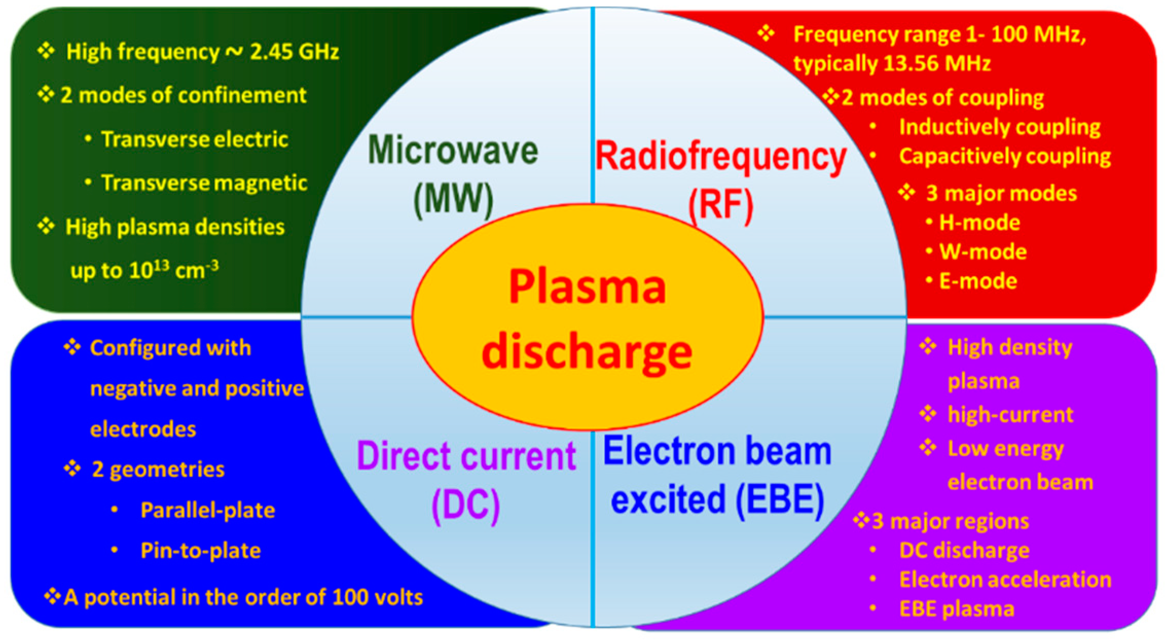
2. Plasma: Potential Approach for Carbon Nanowall (CNW) Synthesis
3. Growth Mechanism of Vertically-Oriented Carbon Nanostructures in Plasma-Enhanced Chemical Vapor Deposition (PECVD)
4. Influence of Gas Sources and Gas Proportion
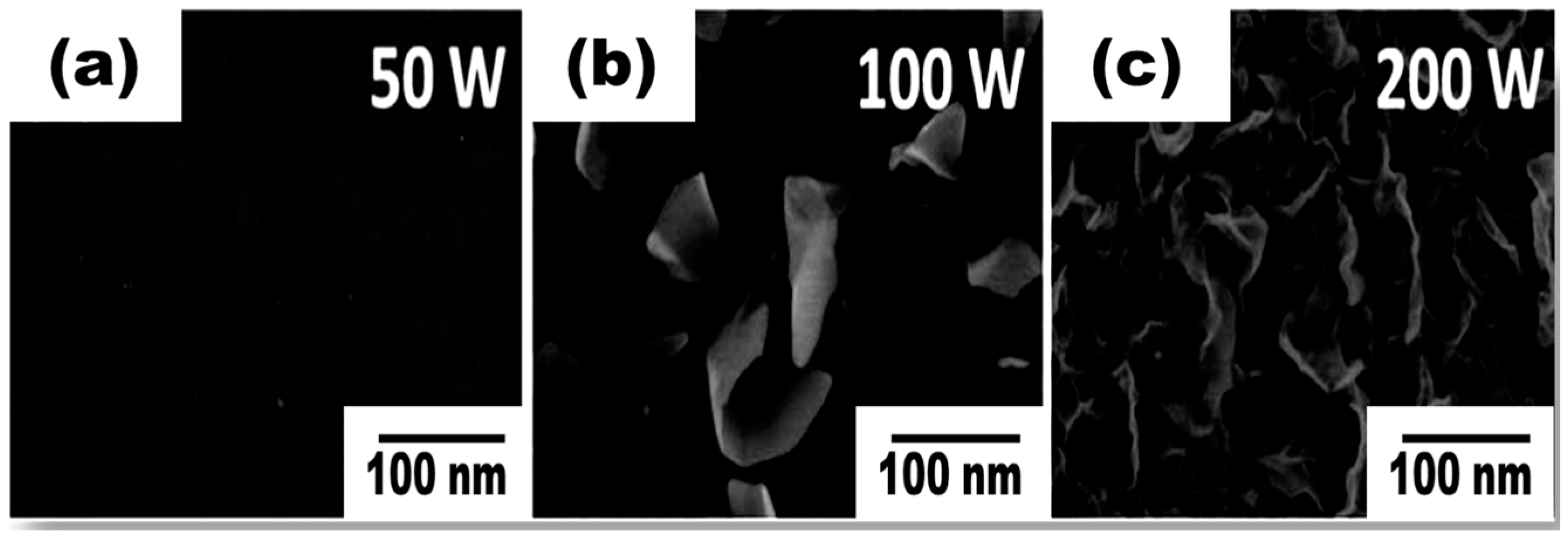
5. Electric Fields and Plasma Power
6. Substrate Temperature
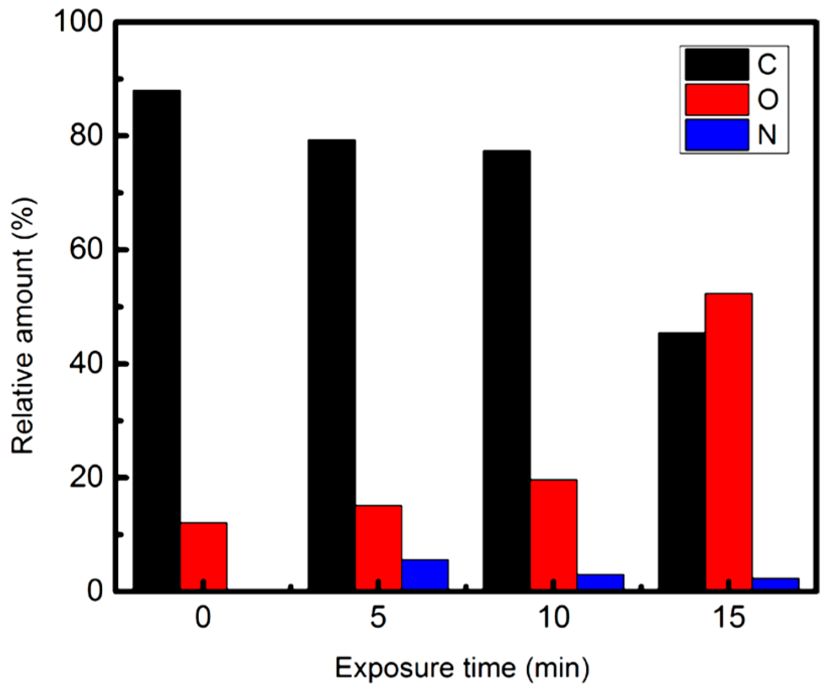
7. Plasma Assisted Surface Modification and Doping
8. Challenges and opportunities
9. Conclusions
Author Contributions
Funding
Conflicts of Interest
References
- Kroto, H.W.; Heath, J.R.; O’Brien, S.C.; Curl, R.F.; Smalley, R.E. C60: Buckminsterfullerene. Nature 1985, 318, 162. [Google Scholar] [CrossRef]
- Ando, Y.; Zhao, X.; Ohkohchi, M. Production of petal-like graphite sheets by hydrogen arc discharge. Carbon N. Y. 1997, 35, 153–158. [Google Scholar] [CrossRef]
- Wu, Y.; Qiao, P.; Chong, T.; Shen, Z. Carbon nanowalls grown by microwave plasma enhanced chemical vapor deposition. Adv. Mater. 2002, 14, 64–67. [Google Scholar] [CrossRef]
- Novoselov, K.S.; Geim, A.K.; Morozov, S.V.; Jiang, D.; Zhang, Y.; Dubonos, S.V.; Grigorieva, I.V.; Firsov, A.A. Electric field in atomically thin carbon films. Science 2004. [Google Scholar] [CrossRef] [PubMed]
- Machino, T.; Takeuchi, W.; Kano, H.; Hiramatsu, M.; Hori, M. Synthesis of platinum nanoparticles on two-dimensional carbon nanostructures with an ultrahigh aspect ratio employing supercritical fluid chemical vapor deposition process. Appl. Phys. Express 2009, 2, 025001. [Google Scholar] [CrossRef]
- Giorgi, L.; Makris, T.D.; Giorgi, R.; Lisi, N.; Salernitano, E. Electrochemical properties of carbon nanowalls synthesized by HF-CVD. Sensors Actuators B Chem. 2007, 126, 144–152. [Google Scholar] [CrossRef]
- Lehmann, K.; Yurchenko, O.; Melke, J.; Fischer, A.; Urban, G. High electrocatalytic activity of metal-free and non-doped hierarchical carbon nanowalls towards oxygen reduction reaction. Electrochim. Acta 2018, 269, 657–667. [Google Scholar] [CrossRef]
- Wu, J.; Shao, Y.; Wang, B.; Ostrikov, K.K.; Feng, J.; Cheng, Q. Plasma-Produced Vertical Carbonous Nanoflakes for Li-Ion Batteries. Plasma Process. Polym. 2016, 13, 1008–1014. [Google Scholar] [CrossRef]
- Tanaike, O.; Kitada, N.; Yoshimura, H.; Hatori, H.; Kojima, K.; Tachibana, M. Lithium insertion behavior of carbon nanowalls by dc plasma CVD and its heat-treatment effect. Solid State Ionics 2009, 180, 381–385. [Google Scholar] [CrossRef]
- Krivchenko, V.A.; Itkis, D.M.; Evlashin, S.A.; Semenenko, D.A.; Goodilin, E.A.; Rakhimov, A.T.; Stepanov, A.S.; Suetin, N.V.; Pilevsky, A.A.; Voronin, P.V. Carbon nanowalls decorated with silicon for lithium-ion batteries. Carbon N. Y. 2012, 50, 1438–1442. [Google Scholar] [CrossRef]
- Dyakonov, P.; Mironovich, K.; Svyakhovskiy, S.; Voloshina, O.; Dagesyan, S.; Panchishin, A.; Suetin, N.; Bagratashvili, V.; Timashev, P.; Shirshin, E.; et al. Carbon nanowalls as a platform for biological SERS studies. Sci. Rep. 2017, 7, 13352. [Google Scholar] [CrossRef] [PubMed]
- Yang, B.; Wu, Y.; Zong, B.; Shen, Z. Electrochemical Synthesis and Characterization of Magnetic Nanoparticles on Carbon Nanowall Templates. Nano Lett. 2002, 2, 751–754. [Google Scholar] [CrossRef]
- Hou, K.; Outlaw, R.A.; Wang, S.; Zhu, M.; Quinlan, R.A.; Manos, D.M.; Kordesch, M.E.; Arp, U.; Holloway, B.C. Uniform and enhanced field emission from chromium oxide coated carbon nanosheets. Appl. Phys. Lett. 2008, 92, 133112. [Google Scholar] [CrossRef]
- Yu, K.; Bo, Z.; Lu, G.; Mao, S.; Cui, S.; Zhu, Y.; Chen, X.; Ruoff, R.S.; Chen, J. Growth of carbon nanowalls at atmospheric pressure for one-step gas sensor fabrication. Nanoscale Res. Lett. 2011, 6, 202. [Google Scholar] [CrossRef] [PubMed] [Green Version]
- Russo, P.; Xiao, M.; Zhou, N.Y. Carbon nanowalls: A new material for resistive switching memory devices. Carbon N. Y. 2017. [CrossRef]
- Wang, J.; Ito, T. CVD growth and field emission characteristics of nano-structured films composed of vertically standing and mutually intersecting nano-carbon sheets. Diam. Relat. Mater. 2007, 16, 589–593. [Google Scholar] [CrossRef]
- Hojati-Talemi, P.; Simon, G.P. Field emission study of graphene nanowalls prepared by microwave-plasma method. Carbon N. Y. 2011, 49, 2875–2877. [Google Scholar] [CrossRef]
- Sankaran, K.J.; Ficek, M.; Kunuku, S.; Panda, K.; Yeh, C.J.; Park, J.Y.; Sawczak, M.; Michałowski, P.P.; Leou, K.C.; Bogdanowicz, R.; et al. Self-organized multi-layered graphene-boron-doped diamond hybrid nanowalls for high-performance electron emission devices. Nanoscale 2018, 10, 1345–1355. [Google Scholar] [CrossRef] [PubMed]
- Vizireanu, S.; Ionita, M.D.; Dinescu, G.; Enculescu, I.; Baibarac, M.; Baltog, I. Post-synthesis carbon nanowalls transformation under hydrogen, oxygen, nitrogen, tetrafluoroethane and sulfur hexafluoride plasma treatments. Plasma Process. Polym. 2012, 9, 363–370. [Google Scholar] [CrossRef]
- Segundo, E.H.; Fontana, L.C.; Recco, A.A.C.; Scholtz, J.S.; Nespolo Vomstein, M.A.; Becker, D. Graphene nanosheets obtained through graphite powder exfoliation in pulsed underwater electrical discharge. Mater. Chem. Phys. 2018, 217, 1–4. [Google Scholar] [CrossRef]
- Chen, Z.; Guo, X.; Zhu, L.; Li, L.; Liu, Y.; Zhao, L.; Zhang, W.; Chen, J.; Zhang, Y.; Zhao, Y. Direct growth of graphene on vertically standing glass by a metal-free chemical vapor deposition method. J. Mater. Sci. Technol. 2018, 34, 1919–1924. [Google Scholar] [CrossRef]
- Chen, J.; Guo, Y.; Wen, Y.; Huang, L.; Xue, Y.; Geng, D.; Wu, B.; Luo, B.; Yu, G.; Liu, Y. Two-stage metal-catalyst-free growth of high-quality polycrystalline graphene films on silicon nitride substrates. Adv. Mater. 2013, 25, 992–997. [Google Scholar] [CrossRef] [PubMed]
- Hwang, J.; Kim, M.; Campbell, D.; Alsalman, H.A.; Kwak, J.Y.; Shivaraman, S.; Woll, A.R.; Singh, A.K.; Hennig, R.G.; Gorantla, S.; et al. Van der waals epitaxial growth of graphene on sapphire by chemical vapor deposition without a metal catalyst. ACS Nano 2013, 7, 385–395. [Google Scholar] [CrossRef] [PubMed]
- Chuang, A.T.H.; Robertson, J.; Boskovic, B.O.; Koziol, K.K.K. Three-dimensional carbon nanowall structures. Appl. Phys. Lett. 2007, 90, 123107. [Google Scholar] [CrossRef]
- Tanaka, K.; Yoshimura, M.; Okamoto, A.; Ueda, K. Growth of carbon nanowalls on a SiO2 substrate by microwave plasma-enhanced chemical vapor deposition. Jpn. J. Appl. Phys. Part 1 Regul. Pap. Short Notes Rev. Pap. 2005, 44, 2074–2076. [Google Scholar] [CrossRef]
- Malesevic, A.; Vitchev, R.; Schouteden, K.; Volodin, A.; Zhang, L.; Van Tendeloo, G.; Vanhulsel, A.; Van Haesendonck, C. Synthesis of few-layer graphene via microwave plasma-enhanced chemical vapour deposition. Nanotechnology 2008, 19, 305604. [Google Scholar] [CrossRef] [PubMed] [Green Version]
- Yamada, T.; Ishihara, M.; Kim, J.; Hasegawa, M.; Iijima, S. A roll-to-roll microwave plasma chemical vapor deposition process for the production of 294mm width graphene films at low temperature. Carbon 2012, 50, 2615–2619. [Google Scholar] [CrossRef]
- Kalita, G.; Wakita, K.; Umeno, M. Low temperature growth of graphene film by microwave assisted surface wave plasma CVD for transparent electrode application. RSC Adv. 2012, 2, 2815. [Google Scholar] [CrossRef]
- Bo, Z.; Yang, Y.; Chen, J.; Yu, K.; Yan, J.; Cen, K. Plasma-enhanced chemical vapor deposition synthesis of vertically oriented graphene nanosheets. Nanoscale 2013, 5, 5180–5204. [Google Scholar] [CrossRef] [PubMed]
- Zhong, Y.L.; Tian, Z.; Simon, G.P.; Li, D. Scalable production of graphene via wet chemistry: Progress and challenges. Mater. Today 2015, 18, 73–78. [Google Scholar] [CrossRef]
- Hiramatsu, M.; Hori, M. Carbon Nanowalls: Synthesis and Emerging Applications; Springer: Wien, Germany, 2010; ISBN 9783211997178. [Google Scholar]
- Woehrl, N.; Ochedowski, O.; Gottlieb, S.; Shibasaki, K.; Schulz, S. Plasma-enhanced chemical vapor deposition of graphene on copper substrates. AIP Adv. 2014, 4, 047128. [Google Scholar] [CrossRef] [Green Version]
- Lieberman, M.A.; Lichtenberg, A.J. Principles of Plasma Discharges and Materials Processing: Second Edition; John Wiley & Sons, Inc.: Hoboken, NJ, USA, 2005; ISBN 0471720011. [Google Scholar]
- Wang, Q.; Wang, X.; Chai, Z.; Hu, W. Low-temperature plasma synthesis of carbon nanotubes and graphene based materials and their fuel cell applications. Chem. Soc. Rev. 2013, 42, 8821–8834. [Google Scholar] [CrossRef] [PubMed]
- Conrads, H.; Schmidt, M. Plasma generation and plasma sources. Plasma Sources Sci. Technol. 2000, 9, 441. [Google Scholar] [CrossRef]
- Azarenkov, N.A.; Denisenko, I.B.; Ostrikov, K.N. A model of a large-area planar plasma producer based on surface wave propagation in a plasma-metal structure with a dielectric sheath. J. Phys. D Appl. Phys. 1995, 28, 2465. [Google Scholar] [CrossRef]
- Stratakos, Y.; Zeniou, A.; Gogolides, E. Comparison of Helical and Helicon Antennas as Sources of Plasma Excitation Using a Full Wave 3D Electromagnetic Analysis in Vacuum. Plasma Process. Polym. 2017, 14, 1600107. [Google Scholar] [CrossRef]
- Cheng, Q.; Xu, S.; Ostrikov, K. (Ken) Single-step, rapid low-temperature synthesis of Si quantum dots embedded in an amorphous SiC matrix in high-density reactive plasmas. Acta Mater. 2010, 58, 560–569. [Google Scholar] [CrossRef]
- Li, M.; Liu, D.; Wei, D.; Song, X.; Wei, D.; Wee, A.T.S. Controllable Synthesis of Graphene by Plasma-Enhanced Chemical Vapor Deposition and Its Related Applications. Adv. Sci. 2016, 3, 1600003. [Google Scholar] [CrossRef] [PubMed] [Green Version]
- Hertl, M.; Jolly, J.; Baravian, G. Detection of hydrogen atoms in SiH4-H2radio-frequency plasmas using two-photon laser-induced fluorescence. J. Appl. Phys. 2002, 92, 710–715. [Google Scholar] [CrossRef]
- Hiramatsu, M.; Shiji, K.; Amano, H.; Hori, M. Fabrication of vertically aligned carbon nanowalls using capacitively coupled plasma-enhanced chemical vapor deposition assisted by hydrogen radical injection. Appl. Phys. Lett. 2004, 84, 4708–4710. [Google Scholar] [CrossRef]
- Kondo, S.; Hori, M.; Yamakawa, K.; Den, S.; Kano, H.; Hiramatsu, M. Highly reliable growth process of carbon nanowalls using radical injection plasma-enhanced chemical vapor deposition. J. Vac. Sci. Technol. B Microelectron. Nanom. Struct. 2008, 26, 1294. [Google Scholar] [CrossRef]
- Banerjee, D.; Mukherjee, S.; Chattopadhyay, K.K. Synthesis of amorphous carbon nanowalls by DC-PECVD on different substrates and study of its field emission properties. Appl. Surf. Sci. 2011, 257, 3717–3722. [Google Scholar] [CrossRef]
- Hara, T.; Hamagaki, M.; Sanda, A.; Aoyagi, Y.; Namba, S. New high current low energy ion source. Jpn. J. Appl. Phys. 1986, 25, L252–L253. [Google Scholar] [CrossRef]
- Mori, T.; Hiramatsu, M.; Yamakawa, K.; Takeda, K.; Hori, M. Fabrication of carbon nanowalls using electron beam excited plasma-enhanced chemical vapor deposition. Diam. Relat. Mater. 2008, 17, 1513–1517. [Google Scholar] [CrossRef]
- Levchenko, I.; Cvelbar, U.; Keidar, M. Graphene Flakes in Arc Plasma: Conditions for the Fast Single-Layer Growth. Graphene 2016, 5, 81–89. [Google Scholar] [CrossRef]
- Keidar, M.; Shashurin, A.; Li, J.; Volotskova, O.; Kundrapu, M.; Zhuang, T. Sen Arc plasma synthesis of carbon nanostructures: Where is the frontier? J. Phys. D Appl. Phys. 2011, 44, 174006. [Google Scholar] [CrossRef]
- Kim, Y.; Song, W.; Lee, S.Y.; Jeon, C.; Jung, W.; Kim, M.; Park, C.Y. Low-temperature synthesis of graphene on nickel foil by microwave plasma chemical vapor deposition. Appl. Phys. Lett. 2011, 98, 263106. [Google Scholar] [CrossRef] [PubMed]
- Kondo, S.; Kawai, S.; Takeuchi, W.; Yamakawa, K.; Den, S.; Kano, H.; Hiramatsu, M.; Hori, M. Initial growth process of carbon nanowalls synthesized by radical injection plasma-enhanced chemical vapor deposition. J. Appl. Phys. 2009, 106, 094302. [Google Scholar] [CrossRef]
- Giese, A.; Schipporeit, S.; Buck, V.; Wöhrl, N. Synthesis of carbon nanowalls from a single-source metal-organic precursor. Beilstein J. Nanotechnol. 2018, 9, 1895–1905. [Google Scholar] [CrossRef] [PubMed]
- Park, J.K.; Kang, H.; Kim, J.H.; Choi, W. Improvement of Electrical Properties of Carbon Nanowall by the Deposition of Thin Film. J. Nanosci. Nanotechnol. 2018, 18, 6026–6028. [Google Scholar] [CrossRef] [PubMed]
- Van Nang, L.; Kim, E.-T. Controllable Synthesis of High-Quality Graphene Using Inductively-Coupled Plasma Chemical Vapor Deposition. J. Electrochem. Soc. 2012, 159, K93–K96. [Google Scholar] [CrossRef]
- Wang, J.J.; Zhu, M.Y.; Outlaw, R.A.; Zhao, X.; Manos, D.M.; Holloway, B.C.; Mammana, V.P. Free-standing subnanometer qraphite sheets. Appl. Phys. Lett. 2004, 85, 1265–1267. [Google Scholar] [CrossRef]
- Vizireanu, S.; Nistor, L.; Haupt, M.; Katzenmaier, V.; Oehr, C.; Dinescu, G. Carbon nanowalls growth by radiofrequency plasma-beam-enhanced chemical vapor deposition. Plasma Process. Polym. 2008, 5, 263–268. [Google Scholar] [CrossRef]
- Acosta Gentoiu, M.; Betancourt-Riera, R.; Vizireanu, S.; Burducea, I.; Marascu, V.; Stoica, S.D.; Bita, B.I.; Dinescu, G.; Riera, R. Morphology, Microstructure, and Hydrogen Content of Carbon Nanostructures Obtained by PECVD at Various Temperatures. J. Nanomater. 2017, 2017, 1374973. [Google Scholar] [CrossRef]
- Bo, Z.; Yu, K.; Lu, G.; Wang, P.; Mao, S.; Chen, J. Understanding growth of carbon nanowalls at atmospheric pressure using normal glow discharge plasma-enhanced chemical vapor deposition. Carbon N. Y. 2011, 49, 1849–1858. [Google Scholar] [CrossRef]
- Lehmann, K.; Yurchenko, O.; Urban, G. Effect of the aromatic precursor flow rate on the morphology and properties of carbon nanostructures in plasma enhanced chemical vapor deposition. RSC Adv. 2016, 6, 32779–32788. [Google Scholar] [CrossRef] [Green Version]
- Bundaleska, N.; Henriques, J.; Abrashev, M.; Botelho do Rego, A.M.; Ferraria, A.M.; Almeida, A.; Dias, F.M.; Valcheva, E.; Arnaudov, B.; Upadhyay, K.K.; et al. Large-scale synthesis of free-standing N-doped graphene using microwave plasma. Sci. Rep. 2018, 8, 12595. [Google Scholar] [CrossRef] [PubMed]
- Seo, D.H.; Rider, A.E.; Kumar, S.; Randeniya, L.K.; Ostrikov, K. Vertical graphene gas- and bio-sensors via catalyst-free, reactive plasma reforming of natural honey. Carbon N. Y. 2013, 60, 221–228. [Google Scholar] [CrossRef]
- Seo, D.H.; Pineda, S.; Yick, S.; Bell, J.; Han, Z.J.; Ostrikov, K. Plasma-enabled sustainable elemental lifecycles: Honeycomb-derived graphenes for next-generation biosensors and supercapacitors. Green Chem. 2015, 17, 2164–2171. [Google Scholar] [CrossRef]
- Zhao, J.; Shaygan, M.; Eckert, J.; Meyyappan, M.; Rümmeli, M.H. A growth mechanism for free-standing vertical graphene. Nano Lett. 2014, 14, 3064–3071. [Google Scholar] [CrossRef] [PubMed]
- Bo, Z.; Mao, S.; Jun Han, Z.; Cen, K.; Chen, J.; Ostrikov, K. Emerging energy and environmental applications of vertically-oriented graphenes. Chem. Soc. Rev. 2015, 44, 2108–2121. [Google Scholar] [CrossRef] [PubMed] [Green Version]
- Zhu, M.; Wang, J.; Holloway, B.C.; Outlaw, R.A.; Zhao, X.; Hou, K.; Shutthanandan, V.; Manos, D.M. A mechanism for carbon nanosheet formation. Carbon N. Y. 2007, 45, 2229–2234. [Google Scholar] [CrossRef]
- Hiramatsu, M.; Hori, M. Fabrication of carbon nanowalls using novel plasma processing. Jpn. J. Appl. Phys. Part 1 Regul. Pap. Short Notes Rev. Pap. 2006, 45, 5522–5527. [Google Scholar] [CrossRef]
- Baranov, O.; Levchenko, I.; Xu, S.; Lim, J.W.M.; Cvelbar, U.; Bazaka, K. Formation of vertically oriented graphenes: what are the key drivers of growth? 2D Mater. 2018, 5, 044002. [Google Scholar] [CrossRef]
- Davami, K.; Shaygan, M.; Kheirabi, N.; Zhao, J.; Kovalenko, D.A.; Rümmeli, M.H.; Opitz, J.; Cuniberti, G.; Lee, J.S.; Meyyappan, M. Synthesis and characterization of carbon nanowalls on different substrates by radio frequency plasma enhanced chemical vapor deposition. Carbon N. Y. 2014, 72, 372–380. [Google Scholar] [CrossRef]
- Denysenko, I.; Ostrikov, K.; Yu, M.Y.; Azarenkov, N.A. Effects of ions and atomic hydrogen in plasma-assisted growth of single-walled carbon nanotubes. J. Appl. Phys. 2007, 102, 074308. [Google Scholar] [CrossRef] [Green Version]
- Nozaki, T.; Goto, T.; Okazaki, K.; Ohnishi, K.; Mangolini, L.; Heberlein, J.; Kortshagen, U. Deposition of vertically oriented carbon nanofibers in atmospheric pressure radio frequency discharge. J. Appl. Phys. 2006, 99, 024310. [Google Scholar] [CrossRef]
- Ostrikov, K. Nanoscale transfer of energy and matter in plasma-surface interactions. IEEE Trans. Plasma Sci. 2011, 39, 963–970. [Google Scholar] [CrossRef]
- Mao, M.; Bogaerts, A. Investigating the plasma chemistry for the synthesis of carbon nanotubes/nanofibres in an inductively coupled plasma enhanced CVD system: The effect of different gas mixtures. J. Phys. D Appl. Phys. 2010, 43, 205201. [Google Scholar] [CrossRef]
- Chhowalla, M.; Teo, K.B.K.; Ducati, C.; Rupesinghe, N.L.; Amaratunga, G.A.J.; Ferrari, A.C.; Roy, D.; Robertson, J.; Milne, W.I. Growth process conditions of vertically aligned carbon nanotubes using plasma enhanced chemical vapor deposition. J. Appl. Phys. 2001, 90, 5308–5317. [Google Scholar] [CrossRef]
- Denysenko, I.B.; Xu, S.; Long, J.D.; Rutkevych, P.P.; Azarenkov, N.A.; Ostrikov, K. Inductively coupled Ar/CH4/H2 plasmas for low-temperature deposition of ordered carbon nanostructures. J. Appl. Phys. 2004, 95, 2713–2724. [Google Scholar] [CrossRef] [Green Version]
- Chuang, A.T.H.; Boskovic, B.O.; Robertson, J. Freestanding carbon nanowalls by microwave plasma-enhanced chemical vapour deposition. Diam. Relat. Mater. 2006, 15, 1103–1106. [Google Scholar] [CrossRef]
- Mantzaris, N.V.; Gogolides, E.; Boudouvis, A.G.; Rhallabi, A.; Turban, G. Surface and plasma simulation of deposition processes: CH4plasmas for the growth of diamondlike carbon. J. Appl. Phys. 1996, 79, 3718–3729. [Google Scholar] [CrossRef]
- Teii, K.; Shimada, S.; Nakashima, M.; Chuang, A.T.H. Synthesis and electrical characterization of n -type carbon nanowalls. J. Appl. Phys. 2009, 106, 084303. [Google Scholar] [CrossRef]
- Vizireanu, S.; Stoica, S.D.; Luculescu, C.; Nistor, L.C.; Mitu, B.; Dinescu, G. Plasma techniques for nanostructured carbon materials synthesis. A case study: Carbon nanowall growth by low pressure expanding RF plasma. Plasma Sources Sci. Technol. 2010, 19, 034016. [Google Scholar] [CrossRef]
- Zhu, M.Y.; Outlaw, R.A.; Bagge-Hansen, M.; Chen, H.J.; Manos, D.M. Enhanced field emission of vertically oriented carbon nanosheets synthesized by C2H2/H2 plasma enhanced CVD. Carbon N. Y. 2011, 49, 2526–2531. [Google Scholar] [CrossRef]
- Hiramatsu, M.; Kato, K.; Lau, C.H.; Foord, J.S.; Hori, M. Measurement of C2radical density in microwave methane/hydrogen plasma used for nanocrystalline diamond film formation. Diam. Relat. Mater. 2003, 12, 365–368. [Google Scholar] [CrossRef]
- Shiomi, T.; Nagai, H.; Kato, K.; Hiramatsu, M.; Nawata, M. Detection of C2 radicals in low-pressure inductively coupled plasma source for diamond chemical vapor deposition. Diam. Relat. Mater. 2001, 10, 388–392. [Google Scholar] [CrossRef]
- Hori, M.; Kondo, H.; Hiramatsu, M. Radical-controlled plasma processing for nanofabrication. J. Phys. D Appl. Phys. 2011, 44, 174027. [Google Scholar] [CrossRef]
- Shiji, K.; Hiramatsu, M.; Enomoto, A.; Nakamura, M.; Amano, H.; Hori, M. Vertical growth of carbon nanowalls using rf plasma-enhanced chemical vapor deposition. Diam. Relat. Mater. 2005, 14, 831–834. [Google Scholar] [CrossRef]
- Shang, N.G.; Au, F.C.K.; Meng, X.M.; Lee, C.S.; Bello, I.; Lee, S.T. Uniform carbon nanoflake films and their field emissions. Chem. Phys. Lett. 2002, 358, 187–191. [Google Scholar] [CrossRef]
- Chatei, H.; Belmahi, M.; Assouar, M.B.; Le Brizoual, L.; Bourson, P.; Bougdira, J. Growth and characterisation of carbon nanostructures obtained by MPACVD system using CH4/CO2gas mixture. Diam. Relat. Mater. 2006, 15, 1041–1046. [Google Scholar] [CrossRef]
- Wang, J.; Zhu, M.; Outlaw, R.A.; Zhao, X.; Manos, D.M.; Holloway, B.C. Synthesis of carbon nanosheets by inductively coupled radio-frequency plasma enhanced chemical vapor deposition. Carbon N. Y. 2004, 42, 2867–2872. [Google Scholar] [CrossRef]
- Wu, Y.; Yang, B.; Zong, B.; Sun, H.; Shen, Z.; Feng, Y. Carbon nanowalls and related materials. J. Mater. Chem. 2004, 14, 469–477. [Google Scholar] [CrossRef]
- Kondo, H.; Hori, M.; Hiramatsu, M. Nucleation and Vertical Growth of Nano-Graphene Sheets. In Graphene—Synthesis, Characterization, Properties and Applications; InTech: Rijeka, Croatia, 2011; ISBN 9789533072920. [Google Scholar] [Green Version]
- Suzuki, S.; Chatterjee, A.; Cheng, C.L.; Yoshimura, M. Effect of hydrogen on carbon nanowall growth by microwave plasma-enhanced chemical vapor deposition. Jpn. J. Appl. Phys. 2011, 50, 01AF08. [Google Scholar] [CrossRef]
- Takeuchi, W.; Hiramatsu, M.; Tokuda, Y.; Kano, H.; Hori, M. Control of Structure and Electrical properties of Carbon Nanowalls: Effect of N2/O2 addition to fluorocarbon plasma CVD with H radical injection. In Proceedings of the 2008 International Conference on Solid State Devices and Materials, Tsukuba, Japan, 23–26 September 2008; Volume 2, pp. 126–127. [Google Scholar]
- Paschen, F. Ueber die zum Funkenübergang in Luft, Wasserstoff und Kohlensäure bei verschiedenen Drucken erforderliche Potentialdifferenz. Ann. Phys. 1889, 273, 69–96. [Google Scholar] [CrossRef] [Green Version]
- Hiramatsu, M.; Tomatsu, M.; Kondo, H.; Hori, M. Synthesis of vertical nanographene network as platform for electrochemical applications. In Proceedings of the 2017 World Congress on Advances in Nano, Bio, Robotics and Energy (ANBRE17), Seoul, Korea, 28 August–1 September 2017. [Google Scholar]
- Takeuchi, W.; Sasaki, H.; Kato, S.; Takashima, S.; Hiramatsu, M.; Hori, M. Development of measurement technique for carbon atoms employing vacuum ultraviolet absorption spectroscopy with a microdischarge hollow-cathode lamp and its application to diagnostics of nanographene sheet material formation plasmas. J. Appl. Phys. 2009, 105, 113305. [Google Scholar] [CrossRef]
- Ostrikov, K.; Neyts, E.C.; Meyyappan, M. Plasma nanoscience: From nano-solids in plasmas to nano-plasmas in solids. Adv. Phys. 2013, 62, 113–224. [Google Scholar] [CrossRef]
- Yang, C.; Bi, H.; Wan, D.; Huang, F.; Xie, X.; Jiang, M. Direct PECVD growth of vertically erected graphene walls on dielectric substrates as excellent multifunctional electrodes. J. Mater. Chem. A 2013, 1, 770–775. [Google Scholar] [CrossRef]
- Wiesemann, K. A Short Introduction to Plasma Physics. arXiv, 2014; arXiv:1404.0509. [Google Scholar] [CrossRef]
- Kersten, H.; Deutsch, H.; Steffen, H.; Kroesen, G.M.W.; Hippler, R. The energy balance at substrate surfaces during plasma processing. Vacuum 2001, 63, 385–431. [Google Scholar] [CrossRef]
- Krivchenko, V.; Shevnin, P.; Pilevsky, A.; Egorov, A.; Suetin, N.; Sen, V.; Evlashin, S.; Rakhimov, A. Influence of the growth temperature on structural and electron field emission properties of carbon nanowall/nanotube films synthesized by catalyst-free PECVD. J. Mater. Chem. 2012, 22, 16458–16464. [Google Scholar] [CrossRef]
- Kim, J.; Ishihara, M.; Koga, Y.; Tsugawa, K.; Hasegawa, M.; Iijima, S. Low-temperature synthesis of large-area graphene-based transparent conductive films using surface wave plasma chemical vapor deposition. Appl. Phys. Lett. 2011, 98, 091502. [Google Scholar] [CrossRef]
- Kim, S.Y.; Choi, W.S.; Lee, J.H.; Hong, B. Substrate temperature effect on the growth of carbon nanowalls synthesized via microwave PECVD. Mater. Res. Bull. 2014, 58, 112–116. [Google Scholar] [CrossRef]
- Zeng, L.; Lei, D.; Wang, W.; Liang, J.; Wang, Z.; Yao, N.; Zhang, B. Preparation of carbon nanosheets deposited on carbon nanotubes by microwave plasma-enhanced chemical vapor deposition method. Appl. Surf. Sci. 2008, 254, 1700–1704. [Google Scholar] [CrossRef]
- Felten, A.; Bittencourt, C.; Colomer, J.F.; Van Tendeloo, G.; Pireaux, J.J. Nucleation of metal clusters on plasma treated multi wall carbon nanotubes. Carbon N. Y. 2007, 45, 110–116. [Google Scholar] [CrossRef]
- Jiang, N.; Wang, H.X.; Zhang, H.; Sasaoka, H.; Nishimura, K. Characterization and surface modification of carbon nanowalls. J. Mater. Chem. 2010, 20, 5070–5073. [Google Scholar] [CrossRef]
- Xu, T.; Yang, J.; Liu, J.; Fu, Q. Surface modification of multi-walled carbon nanotubes by O2plasma. Appl. Surf. Sci. 2007, 253, 8945–8951. [Google Scholar] [CrossRef]
- Nourbakhsh, A.; Cantoro, M.; Vosch, T.; Pourtois, G.; Clemente, F.; Van Der Veen, M.H.; Hofkens, J.; Heyns, M.M.; De Gendt, S.; Sels, B.F. Bandgap opening in oxygen plasma-treated graphene. Nanotechnology 2010, 21, 435203. [Google Scholar] [CrossRef] [PubMed]
- Dias, A.; Bundaleski, N.; Tatarova, E.; Dias, F.M.; Abrashev, M.; Cvelbar, U.; Teodoro, O.M.N.D.; Henriques, J. Production of N-graphene by microwave N2-Ar plasma. J. Phys. D Appl. Phys. 2016, 49, 055307. [Google Scholar] [CrossRef]
- Stancu, E.C.; Stanciuc, A.M.; Vizireanu, S.; Luculescu, C.; Moldovan, L.; Achour, A.; Dinescu, G. Plasma functionalization of carbon nanowalls and its effect on attachment of fibroblast-like cells. J. Phys. D Appl. Phys. 2014, 47, 265203. [Google Scholar] [CrossRef]
- Watanabe, H.; Kondo, H.; Hiramatsu, M.; Sekine, M.; Kumar, S.; Ostrikov, K.; Hori, M. Surface chemical modification of carbon nanowalls for wide-range control of surface wettability. Plasma Process. Polym. 2013, 10, 582–592. [Google Scholar] [CrossRef]
- Zhu, L.; Xiu, Y.; Xu, J.; Tamirisa, P.A.; Hess, D.W.; Wong, C.P. Superhydrophobicity on two-tier rough surfaces fabricated by controlled growth of aligned carbon nanotube arrays coated with fluorocarbon. Langmuir 2005, 21, 11208–11212. [Google Scholar] [CrossRef] [PubMed]
- Lu, C.; Dong, Q.; Tulugan, K.; Park, Y.M.; More, M.A.; Kim, J.; Kim, T.G. Characteristic Study of Boron Doped Carbon Nanowalls Films Deposited by Microwave Plasma Enhanced Chemical Vapor Deposition. J. Nanosci. Nanotechnol. 2016, 16, 1680–1684. [Google Scholar] [CrossRef] [PubMed]
- Tang, Y.B.; Yin, L.C.; Yang, Y.; Bo, X.H.; Cao, Y.L.; Wang, H.E.; Zhang, W.J.; Bello, I.; Lee, S.T.; Cheng, H.M.; et al. Tunable band gaps and p-type transport properties of boron-doped graphenes by controllable ion doping using reactive microwave plasma. ACS Nano 2012, 6, 1970–1978. [Google Scholar] [CrossRef] [PubMed]
- Sobaszek, M.; Siuzdak, K.; Ryl, J.; Sawczak, M.; Gupta, S.; Carrizosa, S.B.; Ficek, M.; Dec, B.; Darowicki, K.; Bogdanowicz, R. Diamond Phase (sp3-C) Rich Boron-Doped Carbon Nanowalls (sp2-C): Physicochemical and Electrochemical Properties. J. Phys. Chem. C 2017, 121, 20821–20833. [Google Scholar] [CrossRef]
- Pham, V.P.; Kim, K.H.; Jeon, M.H.; Lee, S.H.; Kim, K.N.; Yeom, G.Y. Low damage pre-doping on CVD graphene/Cu using a chlorine inductively coupled plasma. Carbon N. Y. 2015, 95, 664–671. [Google Scholar] [CrossRef]
- Vizireanu, S.; Mitu, B.; Luculescu, C.R.; Nistor, L.C.; Dinescu, G. PECVD synthesis of 2D nanostructured carbon material. Surf. Coatings Technol. 2012, 211, 2–8. [Google Scholar] [CrossRef]
- Krivchenko, V.A.; Evlashin, S.A.; Mironovich, K.V.; Verbitskiy, N.I.; Nefedov, A.; Wöll, C.; Kozmenkova, A.Y.; Suetin, N.V.; Svyakhovskiy, S.E.; Vyalikh, D.V.; et al. Carbon nanowalls: The next step for physical manifestation of the black body coating. Sci. Rep. 2013, 3, 3328. [Google Scholar] [CrossRef] [PubMed]
- Liu, R.; Chi, Y.; Fang, L.; Tang, Z.; Yi, X. Synthesis of Carbon Nanowall by Plasma-Enhanced Chemical Vapor Deposition Method. J. Nanosci. Nanotechnol. 2014, 14, 1647–1657. [Google Scholar] [CrossRef] [PubMed]
- Ryu, S.; Han, M.Y.; Maultzsch, J.; Heinz, T.F.; Kim, P.; Steigerwald, M.L.; Brus, L.E. Reversible basal plane hydrogenation of graphene. Nano Lett. 2008, 8, 4597–4602. [Google Scholar] [CrossRef] [PubMed]
- Eren, B.; Fu, W.; Marot, L.; Calame, M.; Steiner, R.; Meyer, E. Spectroscopic ellipsometry on Si/SiO2/graphene tri-layer system exposed to downstream hydrogen plasma: Effects of hydrogenation and chemical sputtering. Appl. Phys. Lett. 2015, 106, 011904. [Google Scholar] [CrossRef] [Green Version]
- Guo, M.; Diao, D.; Fan, X.; Yang, L.; Yu, L. Scratch behavior of re-structured carbon coating by oxygen plasma etching technology for magnetic disk application. Surf. Coat. Technol. 2014, 251, 128–134. [Google Scholar] [CrossRef]
- Ion, R.; Vizireanu, S.; Stancu, C.E.; Luculescu, C.; Cimpean, A.; Dinescu, G. Surface plasma functionalization influences macrophage behavior on carbon nanowalls. Mater. Sci. Eng. C 2015, 48, 118–125. [Google Scholar] [CrossRef] [PubMed]
- Wu, Y.H.; Yang, B.J.; Han, G.C.; Zong, B.Y.; Ni, H.Q.; Luo, P.; Chong, T.C.; Low, T.S.; Shen, Z.X. Fabrication of a class of nanostructured materials using carbon nanowalls as the templates. Adv. Funct. Mater. 2002, 12, 489–494. [Google Scholar] [CrossRef]
- Gokus, T.; Nair, R.R.; Bonetti, A.; Böhmler, M.; Lombardo, A.; Novoselov, K.S.; Geim, A.K.; Ferrari, A.C.; Hartschuh, A. Making graphene luminescent by oxygen plasma treatment. ACS Nano 2009, 3, 3963–3968. [Google Scholar] [CrossRef] [PubMed] [Green Version]
- Kanghyun, K.; Hyung, J.P.; Woo, B.C.; Kook, J.K.; Gyu, T.K.; Wan, S.Y. Electric property evolution of structurally defected multilayer grapheme. Nano Lett. 2008, 8, 3092–3096. [Google Scholar] [CrossRef]
- Thiyagarajan, K.; Saravanakumar, B.; Kim, S.J. Gate-tunable photoresponse of defective graphene: From ultraviolet to visible. ACS Appl. Mater. Interfaces 2015, 7, 2171–2177. [Google Scholar] [CrossRef] [PubMed]
- Liu, J.; Zeng, B.; Wu, Z.; Zhu, J.; Liu, X. Improved field emission property of graphene paper by plasma treatment. Appl. Phys. Lett. 2010, 97, 033109. [Google Scholar] [CrossRef]
- Kondo, S.; Kondo, H.; Hiramatsu, M.; Sekine, M.; Hori, M. Critical factors for nucleation and vertical growth of two dimensional nano-graphene sheets employing a novel Ar+beam with hydrogen and fluorocarbon radical injection. Appl. Phys. Express 2010, 3, 045102. [Google Scholar] [CrossRef]
- Qi, J.L.; Wang, X.; Zheng, W.T.; Tian, H.W.; Hu, C.Q.; Peng, Y.S. Ar plasma treatment on few layer graphene sheets for enhancing their field emission properties. J. Phys. D Appl. Phys. 2010, 43, 055302. [Google Scholar] [CrossRef]
- Takeuchi, W.; Ura, M.; Hiramatsu, M.; Tokuda, Y.; Kano, H.; Hori, M. Electrical conduction control of carbon nanowalls. Appl. Phys. Lett. 2008, 92, 213103. [Google Scholar] [CrossRef]
- Wang, C.D.; Yuen, M.F.; Ng, T.W.; Jha, S.K.; Lu, Z.Z.; Kwok, S.Y.; Wong, T.L.; Yang, X.; Lee, C.S.; Lee, S.T.; et al. Plasma-assisted growth and nitrogen doping of graphene films. Appl. Phys. Lett. 2012, 100, 253107. [Google Scholar] [CrossRef]
- Takeuchi, W.; Kondo, H.; Obayashi, T.; Hiramatsu, M.; Hori, M. Electron field emission enhancement of carbon nanowalls by plasma surface nitridation. Appl. Phys. Lett. 2011, 98, 123107. [Google Scholar] [CrossRef]
- McClure, J.P.; Thornton, J.D.; Jiang, R.; Chu, D.; Cuomo, J.J.; Fedkiw, P.S. Oxygen Reduction on Metal-Free Nitrogen-Doped Carbon Nanowall Electrodes. J. Electrochem. Soc. 2012, 159, F733–F742. [Google Scholar] [CrossRef]
- Cho, H.J.; Kondo, H.; Ishikawa, K.; Sekine, M.; Hiramatsu, M.; Hori, M. Effects of nitrogen plasma post-treatment on electrical conduction of carbon nanowalls. Jpn. J. Appl. Phys. 2014, 53, 040307. [Google Scholar] [CrossRef]
- Zhou, Y.; Wang, B.; Zhang, X.; Zhao, M.; Li, E.; Yan, H. The modifications of the surface wettability of amorphous carbon films. Colloids Surf. A Physicochem. Eng. Asp. 2009, 335, 128–132. [Google Scholar] [CrossRef]
- Fan, L.; Zhang, H.; Zhang, P.; Sun, X. One-step synthesis of chlorinated graphene by plasma enhanced chemical vapor deposition. Appl. Surf. Sci. 2015, 347, 632–635. [Google Scholar] [CrossRef]
- Elias, D.C.; Nair, R.R.; Mohiuddin, T.M.G.; Morozov, S.V.; Blake, P.; Halsall, M.P.; Ferrari, A.C.; Boukhvalov, D.W.; Katsnelson, M.I.; Geim, A.K.; et al. Control of Graphene’s Properties by Reversible Hydrogenation: Evidence for Graphane. Science 2009, 323, 610–613. [Google Scholar] [CrossRef] [PubMed]
- Watanabe, H.; Kondo, H.; Sekine, M.; Hiramatsu, M.; Hori, M. Control of super hydrophobic and super hydrophilic surfaces of carbon nanowalls using atmospheric pressure plasma treatments. Jpn. J. Appl. Phys. 2012, 51, 01AJ07. [Google Scholar] [CrossRef]
- Cui, L.; Chen, J.; Yang, B.; Sun, D.; Jiao, T. RF-PECVD synthesis of carbon nanowalls and their field emission properties. Appl. Surf. Sci. 2015, 357, 1–7. [Google Scholar] [CrossRef]
- Sahoo, G.; Polaki, S.R.; Ghosh, S.; Krishna, N.G.; Kamruddin, M.; Ostrikov, K. (Ken) Plasma-tuneable oxygen functionalization of vertical graphenes enhance electrochemical capacitor performance. Energy Storage Mater. 2018, 14, 297–305. [Google Scholar] [CrossRef]
- Sahoo, G.; Polaki, S.R.; Ghosh, S.; Krishna, N.G.; Kamruddin, M. Temporal-stability of plasma functionalized vertical graphene electrodes for charge storage. J. Power Sources 2018, 401, 37–48. [Google Scholar] [CrossRef]
- Chen, Q.; Sun, T.; Song, X.; Ran, Q.; Yu, C.; Yang, J.; Feng, H.; Yu, L.; Wei, D. Flexible electrochemical biosensors based on graphene nanowalls for the real-time measurement of lactate. Nanotechnology 2017, 28, 315501. [Google Scholar] [CrossRef] [PubMed] [Green Version]
- Wang, Y.; Li, J.; Song, K. Study on formation and photoluminescence of carbon nanowalls grown on silicon substrates by hot filament chemical vapor deposition. J. Lumin. 2014, 149, 258–263. [Google Scholar] [CrossRef]
- Tatarova, E.; Dias, A.; Henriques, J.; Abrashev, M.; Bundaleska, N.; Kovacevic, E.; Bundaleski, N.; Cvelbar, U.; Valcheva, E.; Arnaudov, B.; et al. Towards large-scale in free-standing graphene and N-graphene sheets. Sci. Rep. 2017, 7, 10175. [Google Scholar] [CrossRef] [PubMed]
- Chi, Y.W.; Hu, C.C.; Shen, H.H.; Huang, K.P. New Approach for High-Voltage Electrical Double-Layer Capacitors Using Vertical Graphene Nanowalls with and without Nitrogen Doping. Nano Lett. 2016, 16, 5719–5727. [Google Scholar] [CrossRef] [PubMed]
- Yen, H.F.; Horng, Y.Y.; Hu, M.S.; Yang, W.H.; Wen, J.R.; Ganguly, A.; Tai, Y.; Chen, K.H.; Chen, L.C. Vertically aligned epitaxial graphene nanowalls with dominated nitrogen doping for superior supercapacitors. Carbon 2015, 82, 124–134. [Google Scholar] [CrossRef]
- Wang, B.B.; Cheng, Q.J.; Wang, L.H.; Zheng, K.; Ostrikov, K. The effect of temperature on the mechanism of photoluminescence from plasma-nucleated, nitrogenated carbon nanotips. Carbon 2012, 50, 3561–3571. [Google Scholar] [CrossRef]
- Bundaleska, N.; Bundaleski, N.; Dias, A.; Dias, F.M.; Abrashev, M.; Filipič, G.; Cvelbar, U.; Rakočević, Z.; Kissovski, Z.; Henriques, J.; et al. Microwave N2-Ar plasmas applied for N-graphene post synthesis. Mater. Res. Express 2018, 5, 095605. [Google Scholar] [CrossRef]


| Plasma Source | Source Gas | Parameters | Nanostructure and Characteristics | Ref. | ||||
|---|---|---|---|---|---|---|---|---|
| Temperature (°C) | Pressure (Torr) | Flow Rate (sccm) | Growth Time (min) | Power (W) | ||||
| MW | CH4:H2 | 650–700 | 1 | 40:10 | 8–10 | 500 | CNW, Uniformly oriented carbon sheets | [3] |
| acetylene, ammonia | High | 10 | Flow ratio <1 | 10 | 500 | CNW, Grape like and aggregate structure | [24] | |
| H2, CH4 | - | 1.7 | 80:20 and 80: 5 | 0.17–15 | 500 | CNWs with a higher growth rate | [25] | |
| CH4/H2 | 700 | 40 | 200 sccm Ratio: 1:8 | 1–50 | 2000 | FLG, vertically-aligned sheets with thickness 4–6 atomic layers | [26] | |
| CH4/H2 | 350 | 2.2 × 10⁻³ | - | 10 | 1300 | CNWs with 660 nm height | [51] | |
| CH4, H2, Ar | 100–400 | <1 Torr | 30, 50, 20 | 1–2 | 16,000 | Graphene sheets, A continuous graphene film with 294 mm width | [27] | |
| C2H2:Ar | 240 | <1 Torr | 10, 200 | 2–4 | 1200 | Few layer graphene sheets with pacing 0.345 nm | [28] | |
| CH4/H2 | 450–700 | 20 | 80:1 | 1 | 1400 | High-quality centimeter scale graphene sheet | [48] | |
| He, H2, CH4 | 680 | atm | 1, 25, 25 | 30 | 350 | Vertically grown carbon nanowall | [31] | |
| RFICP | CH4, H2/Ar | Low | 1 | 1100 | 0–60 | 600 | High-quality graphene layers with significant growth kinetics | [52] |
| CH4/H2 | 680 | 90 mTorr | 0:100–95:5 | - | 900 | Free-standing sub-nanometer graphite sheets | [53] | |
| CH4, Ar | 700–850 | 10–60 mTorr | 7, 1.4 | 30–60 | 500 | The growth of carbon nanowalls | [45] | |
| Al(acac)3, Ar | 350, 425, 500 | 8 Pa | 1.66, 40 | 50 | 500 | CNWs with different structures | [50] | |
| RFCCP | C2F6, CH4, CHF3, C4F6, and H2 | 500 | 100 mTorr | Carbon precursor: 15, and 30 | 3–8 h | 400 | Vertical growth of carbon nanowalls | [41] |
| C2F6, H2 (Radical injection) | 600 | 0.1–1.2 | 50, 100 | 30 Min–10 h | MW/VHF 250/300 | The highly reliable growth of carbon nanowall | [42] | |
| C2F6, H2 | 580 | 1.2 | 50, 100 | 30 s to 60 min | MW/VHF 250/270 | Vertically standing CNWs with a uniform height | [49] | |
| RF plasma beam | C2H2, H2, Ar | 700 | 00075–2.25 | 1–20, 1–20, 100–1000 | 60 | 50–500 | CNWs with large surface area and sharp edges | [54] |
| Ar, H2, C2H2 | 200–700 | 1 | 1050, 25, 1 | 60 | 300 | Various nanostructures including CNWs | [55] | |
| EBEP | CH4/H2 | 570 | 10–30 mTorr | - | 10–90 | Electron-voltage ~60–100 V | Vertically aligned well definite CNW | [45] |
| DC | Ar:H2, CH4, Ar | 700 | atm | 1000, 0.15, 1.35 | 30 s–10 | 0–10 kV | CNWs | [56] |
| Precursor | Flow Rate (sccm) | Plasma Source | Structure and Properties | Effect of Radical Species |
|---|---|---|---|---|
| CH4:H2 | 20:80 & 5:80 | MWPECVD | CNWs with higher growth rate with thickness 20 nm | Hydrogen radicals help the plasma ignition and enhance the growth rate by higher carbon dimer density [25] |
| 200 sccm Ratio: 1:8 | MWPECVD | FLG, vertically aligned sheets with thickness 4–6 atomic layers | The average dimensions of the flakes reduce with increase in hydrogen flow compared to CH4 flow rate [26] | |
| 1:80, 1:40, 1:10 | MWPECVD | High-quality centimeter scale graphene sheet | The flow of more CH4 in a ratio of 80:1 leads to the production of high-quality graphene monolayer without defects [48] | |
| 0:100–95:5 | ICPECVD | Free-standing sub-nanometer graphite sheets | H radicals help with producing carbon nanosheets with thickness 1 nm with an average height of 250 nm [53] | |
| - | EBEPECVD | Vertically aligned well definite CNW | The height of the CNW increased by 3 times and spacing between individual layers increased by 5–10 times [45] | |
| CH4, H2, Ar | 3–7.5, 12.4, 10–50 | ICPECVD | Ordered carbon nanostructures | The electron density growth influenced by the rise of argon density [72] |
| CH4 & Ar:H2 | 1 & 100 (90:10) | ICPECVD | High-quality graphene layers with significant growth kinetics | A single layer of graphene sheets formed due to the high H radical density with help to etch C atoms [52] |
| Ar:H2, CH4: Ar, OH radicals | 1000, 0.15:1.35 | DC-atm | CNWs | OH radicals effectively remove a-C, increases CNW crystallinity and enhance the initial nucleation process [56] |
| CH4, Ar | 7, 1.4 | ICPECVD | The growth of carbon nanowalls | H and Ar radical helps to remove the amorphous carbon and CNW with a smooth surface, saturated morphology and thickness grown [31] |
| C2F6, CH4, CHF3, C4F6, and H2 | 15, and 30 | CCPECVD | Vertical growth of carbon nanowalls | Injection of H radicals to the fluorocarbon radicals produce sp2 bonds on the surface and form a continuous network to form CNW [41] |
| C2F6, H2, O2 | 50, 100, 256 | CCPECVD | The highly reliable growth of carbon nanowall | O2 plasma chamber cleaning increases the growth of CNWs with good reproducibility [42] |
| C2F6, H2, O2 | 50, 100, 5 | CCPECVD (Radical injection) | Vertically standing CNWs with a uniform height | O2 influence the effective removal of amorphous carbon from the CNW surface and controlling the nucleation [49] |
| H2, C2H2:NH3 | 100, Ratio < 1 | DCPECVD | Vertically aligned carbon nanostructures | The high amount of NH3 in the system increases the etching rate by producing large H radicals and remove amorphous carbon between the structures [73] |
| Plasma Treatment | Morphology | Changes in the Structure/Property | Ref. |
|---|---|---|---|
| Hydrogen | FLGs | Few layers of highly crystalline graphene sheets with few defects | [26] |
| Petal-like nanosheets | Carbon nanosheets from CNTs with a thickness 300 to 500 nm | [99] | |
| CNWs | Large area free standing CNWs in a well-isolated manner | [112] | |
| Thin CNW films with ultra-low total reflectance (0.13%) for black body coating | [113] | ||
| Controllable high-quality growth with good electric performance | [114] | ||
| Few-layer graphene | Semiconducting sheets with one magnitude less carrier mobility and two order increase in sheet resistance | [115] | |
| Thin layer graphene sheets | Defects due to hydrogen plasma make fluctuations in optical properties | [116] | |
| CNWs | A surface roughened layer formed with a higher surface area | [101] | |
| Oxygen | Thin carbon films | Re-structured carbon coatings with higher scratch resistance | [117] |
| CNWs | Alters the adhesive macrophage properties | [118] | |
| CNWs | Increasing the surface activity of CNWs to act as a template for fabricating nanostructured materials | [119] | |
| CNWs | O2 plasma addition effectively increases the graphitization of carbon nanowalls and controlling the nucleation of CNW growth | [49] | |
| Few graphene sheets | Enhancing the p-type semiconducting behaviors of graphene nanosheets with strong photoluminescence effect | [120] | |
| Multilayer graphene sheets | The exponential decrease of conductance and transconductance | [121] | |
| Graphene sheets | Transformation of semi-metallic nature of graphene sheets into semiconducting via the opening of a band gap | [103] | |
| Argon | Single layer graphene | Increases the photoresponse by Ar plasma-induced defects | [122] |
| Graphene paper | Reduced the aggregation and forms surface protrusions and improves field emission properties | [123] | |
| CNW | Induce dangling bonds on the surface and resulting in the formation of nucleation sites | [124] | |
| GNWs | Field emission properties of GNWs increases by improving graphitic order and removing impurities | [17] | |
| CNWs | Continuous change in the morphology from 1D to 2D with an increase in Ar flow | [54] | |
| FLGs | Field emission properties enhanced by forming sharp edges and defects | [125] | |
| Nitrogen | CNWs | Electrical conductance of N-doped CNWs increases compared to undoped CNWs, N-doped CNWs exhibits n-type conduction, N act as donor | [126] |
| Graphene sheets | Varying p-type conducting behavior to n-type with increasing N-concentration and possess spin-polarized band structure | [127] | |
| CNWs | n-type conductivity ranging from 1.9 to 330 Ω−1 cm−1 due to nitrogen incorporated defects in the amorphous carbon | [75] | |
| CNWs | The drastic increase in the electron emission current from the CNW edges treatment from 1 to 100 µA | [128] | |
| CNWs | Higher electrochemical reactivity for the N-doped CNWs | [129] | |
| CNWs | Maintain p-type conducting behavior and increases the carrier mobility | [130] | |
| Other plasmas | Fluorination in the a-C | Hydrophobicity of a-C films enhanced by fluorinated plasma treatments | [131] |
| Boron-doped graphene | The bandgap of the B-doped graphene widened to 0.54 eV from 0 eV | [109] | |
| Chlorinated graphene sheets | The large surface area with uniform morphology and possess a p-type semiconducting behavior | [132] | |
| Chlorinated graphene sheets | Reduces the sheet resistance and enhance optical transparency via C-Cl bonds | [111] |
© 2018 by the authors. Licensee MDPI, Basel, Switzerland. This article is an open access article distributed under the terms and conditions of the Creative Commons Attribution (CC BY) license (http://creativecommons.org/licenses/by/4.0/).
Share and Cite
Santhosh, N.M.; Filipič, G.; Tatarova, E.; Baranov, O.; Kondo, H.; Sekine, M.; Hori, M.; Ostrikov, K.; Cvelbar, U. Oriented Carbon Nanostructures by Plasma Processing: Recent Advances and Future Challenges. Micromachines 2018, 9, 565. https://doi.org/10.3390/mi9110565
Santhosh NM, Filipič G, Tatarova E, Baranov O, Kondo H, Sekine M, Hori M, Ostrikov K, Cvelbar U. Oriented Carbon Nanostructures by Plasma Processing: Recent Advances and Future Challenges. Micromachines. 2018; 9(11):565. https://doi.org/10.3390/mi9110565
Chicago/Turabian StyleSanthosh, Neelakandan M., Gregor Filipič, Elena Tatarova, Oleg Baranov, Hiroki Kondo, Makoto Sekine, Masaru Hori, Kostya (Ken) Ostrikov, and Uroš Cvelbar. 2018. "Oriented Carbon Nanostructures by Plasma Processing: Recent Advances and Future Challenges" Micromachines 9, no. 11: 565. https://doi.org/10.3390/mi9110565
APA StyleSanthosh, N. M., Filipič, G., Tatarova, E., Baranov, O., Kondo, H., Sekine, M., Hori, M., Ostrikov, K., & Cvelbar, U. (2018). Oriented Carbon Nanostructures by Plasma Processing: Recent Advances and Future Challenges. Micromachines, 9(11), 565. https://doi.org/10.3390/mi9110565