Abstract
Dislocations play a crucial role in self-organization and strain relaxation mechanisms in SiGe heterostructures. In most cases, they should be avoided, and different strategies exist to exploit their nucleation properties in order to manipulate their position. In either case, detailed knowledge about their exact Burgers vectors and possible dislocation reactions are necessary to optimize the fabrication processes and the properties of SiGe materials. In this review a brief overview of the dislocation mechanisms in the SiGe system is given. The method of choice for dislocation characterization is transmission electron microscopy. In particular, the article provides a detailed introduction into large-angle convergent-beam electron diffraction, and gives an overview of different application examples of this method on SiGe structures and related systems.
1. Introduction
Silicon technology will continue to be the leading technology for micro- and nanoelectronics in the future. A key to further develop this technology is the combination of the Si base material with other materials to adjust or modify its properties. For instance, bonding allows the combination of several different insulators or semiconductor materials like SiO2, GaAs or SiC with silicon [1,2,3]. Epitaxial methods, like chemical vapor deposition or molecular beam epitaxy, are the methods of choice for the fabrication of coherent heterostructures based on silicon substrates [4,5,6]. Important material combinations are fabricated with lattice constant mismatch epitaxy of group IV elements, such as SiGe or SiGeSn [7,8,9,10], which have been the focus of semiconductor research for decades. In addition to combining different materials, nanostructuring is employed to further adapt the electronic and optical properties. This also includes self-organization effects, such as the formation of Stranski–Krastanov (SK) islands. Typical applications are silicon photonics [9,11,12], whereas SK structures, randomly distributed or site controlled on patterned substrates, are promising candidates for efficient light sources [13,14,15]. However, standard SK islands turned out to be disadvantageous because of weak carrier confinement and unfavorable band alignment [16]. Nevertheless, there are current concepts to overcome these challenges with modified Ge quantum dots containing well-defined defects [17,18]. Typical further applications of SiGe heterostructures are Ge as stressors to adapt the charge carrier mobility in field effect transistors [19,20,21] and thermo-electric applications to reduce thermal conductivity due to increased effective phonon scattering in SiGe structures [22,23,24]. Crucial for such lattice misfit structures is the control of potential dislocation structures, which requires efficient dislocation characterization techniques.
In this review, concepts of SiGe heterostructures are presented, where handling and engineering of dislocations are an important part of the research challenge. The characterization of these different dislocation systems with transmission electron microscopy (TEM) is highlighted to give a brief overview of different TEM characterization techniques. The review discusses how three-dimensional information about dislocations is gained in a simple way. Besides more complicated tomography methods, this is achieved usually by using two sets of specimens: Plan-view imaging gives an overview of the dislocation types and distribution with dark- and bright-field imaging, while cross-sectional specimens can be used for a detailed investigation with high-resolution (HRTEM) imaging by phase contrast or scanning methods. Depending on the accessible crystallographic orientations, HRTEM images can be used to determine structures and Burgers vectors of dislocations directly [25,26,27,28,29,30]. The availability of high-end, aberration-corrected microscopes has led to a deeper understanding of dislocations in the SiGe system in recent years by direct investigations of dislocation cores [31,32,33].
The main drawback of employing HRTEM for dislocation analysis is that the investigations very often require complex interpretation and simulations. Additionally, HRTEM imaging has the highest demands regarding the quality of the thin foil specimens, which often can only be reached for very small sample areas leading to weak statistical information. Better statistics can be gained by conventional imaging methods and the g·b analysis that employ thicker specimens with lower quality. This technique is performed by conventional dark- or bright-field imaging, using imaging with well-defined diffraction vectors g to determine the Burgers vectors b of a set of dislocations. An additional, efficient method to exploit this g·b criterion is large-angle convergent-beam electron diffraction (LACBED), which is a defocused convergent-beam electron diffraction (CBED) technique [34]. Here, splittings of hkl Bragg diffraction lines in the LACBED diffraction pattern occur at crossings with dislocation lines in the also present shadow image of the sample. These splittings are then used to determine the Burgers vectors in orientation, sign and amplitude. The aim of this article is to show the potential of LACBED for dislocation characterization in SiGe structures and related systems.
2. Dislocations in SiGe Heterostructures
The method of choice for the fabrication of SiGe heterostructures is epitaxy, which is usually a non-equilibrium process. Kinetics, such as diffusion, nucleation probability and adsorption mechanisms, play an important role in structure formation. Nevertheless, self-organization in SiGe structures is often governed by energy minimization, as described by Gibbs free energy with its parameters like strain–stress state, chemical potential and surface, interface, as well as dislocation energies. A well-studied self-organization effect of thin epitaxial layers are SK islands, which nucleate through a strain relaxation mechanism after the formation of a thin wetting layer (WL) due to an interplay between surface, interface and strain energy [35,36]. A complication is that Si and Ge are fully miscible, and this intermixing influences the interface and surface energies and the built-in strain, which are the key parameters to understand self-organization but also relaxation via dislocations. The strain and composition distributions can be determined for instance with X-ray diffraction methods, leading to average strain values over large areas. Analysis of HRTEM images, on the other hand, are used to directly measure the strain in single structures or near dislocations [25,37,38]. Very often, a combination of both techniques leads to complementary results, allowing for a better understanding of the alloying properties of such systems, as for instance in the comprehensive structural investigation of the wetting layer and the island growth of Ge on Si [36].
For thick SiGe layers, grown at high growth rates, strain relaxation with dislocations is present. Generally, dislocations are described by the line vector l parallel to the line defect and the Burgers vector b that describes the dislocation of the crystal lattice at the line defect position. For a perfect edge dislocation, b equals a full lattice vector and is perpendicular to the line vector l. Such a dislocation can be directly identified in high-resolution TEM images by the presence of an additional lattice half-plane when looking along the line vector, which also allows the direct determination of the Burgers vector [25]. The second type of dislocations are screw dislocations, for which b and l are parallel. Very often, mixed type dislocations are present, which contain an edge and a screw component. If the Burgers vector does not equal an integer lattice parameter, the stacking order is not conserved and a stacking fault (SF) is formed that accompanies these so-called partial dislocations. For the diamond lattice structure of SiGe, perfect 60° mixed-type dislocations with Burgers vectors of on {111} planes, sketched in Figure 1a, define the primary glide system. For the screw (bs), misfit (bm) and tilt (bt) components are shown. The parameters bm and bt represent edge components that can be assigned to crystal misfit and tilt for lattice mismatched layers on (001) substrates for the SiGe system. Perfect dislocations can also dissociate into partial dislocations, indicated in Figure 1a for the perfect dislocation with and . These partial dislocations are 30° and 90° partials, respectively, defined by the angle of the Burgers vector to the line vector .
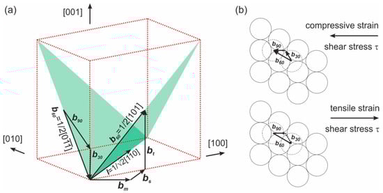
Figure 1.
(a) SiGe unit cell with two {111} glide planes containing two perfect 60° mixed dislocations with a line vector l and Burgers vectors b60. In (b) the two cases of a dislocation glide on a {111} plane of a (001) grown heterostructure with compressive and tensile strain are shown.
The nucleation of dislocations, in particular misfit dislocations for lattice mismatch epitaxy, strongly depends on the resolved shear stress in the primary glide system. Generally, dislocations are only generated if the resolved sheer stress in the glide plane is high enough to reach the critical value for the dislocation to glide. In the SiGe system, the glide of perfect 60° dislocations happen via the two partials shown in Figure 1b. What kind of partial dislocations is formed first depends strongly on the strain and its orientation with respect to the primary glide system that defines the sign and the magnitude of the resolved sheer stress [39,40,41,42]. The dislocation glide of a perfect dislocation with Burgers vector happens via the partial dislocation and by a one, sketched in Figure 1b. The crystal system of Ge on (001) Si is a compressive strained one. The force acting on the partial dislocations is proportional to τ·b. Thus, for the compressive strain case, first a higher strain has to build up for the 30° partial to glide, which is immediately followed by the 90° partial, on which the larger force acts. In the opposite case, in a tensile strained Si layer on (001) Ge, the 90° partial nucleates first at lower shear stress compared to the nucleation of the 30° one of the compressive strain case. That is why the 30° partial dislocation cannot follow immediately (indicated by the dashed vector in Figure 1b) for the tensile strain case, leading to a dissociation and the formation of an extended SF.
This is the reason why the presence of compressive or tensile strain strongly influences the type of generated dislocations and the main reason why the growth of tensile strained Si on (001) SiGe leads to defected structures with SFs [43,44]. Pachinger et al. [45,46] compared the SK dot formation of Si on Ge with the standard SK growth of Ge on Si, showing the importance of the sign of the built-in strain. Ge on Si is compressively strained; while Si on Ge is tensile strained. The systems should behave in comparable manner considering energy minimization, because the strain enters into the Gibbs free energy as a squared term, so that the sign plays no role. According to this argument, Si on Ge should form SK dots comparable to the Ge on Si system. However, this does not take into account the sign with respect to the glide plane. The comparison of Ge on Si and Si on Ge is shown in Figure 2, where small coherent Ge pyramids on Si are presented in (a). The coherence is visible by the symmetric strain contrast pattern at the position of the islands, while the WL is dislocation free, and no crosshatch is visible. In contrast, Si on Ge leads to a thick WL with a well-visible dislocation network and islands, visible by the Moiré pattern as displayed in (b). By employing far from equilibrium growth conditions and the addition of Sb as surfactant, it is possible to adjust the growth kinetics and to create Si dots on Ge with a reduced WL. This avoids the dislocation crosshatch in the WL and only the Si islands remain as displayed in (c). However, the general mechanism of the dislocation glide remains the same. For the Si islands Moiré patterns are visible, indicating that the islands are fully relaxed with dislocations at the Ge–Si interface. Due to the easy formation of 90° partials, by the above-described mechanism, an early relaxation by formation of SF takes place. This leads to fully relaxed, but defected, islands. An example of such an island in cross-sectional geometry is shown in Figure 3, where Fourier analysis (FFT) is applied to identify the different dislocation types. Figure 2 and Figure 3 are good examples of how imaging on plan-view specimens and cross-sectional HRTEM gives a good insight into the dislocation system of a SiGe nanostructure.
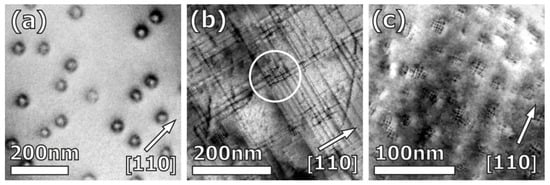
Figure 2.
Comparison of SK dots grown under different conditions: (a) typical, coherent Ge SK islands on Si, (b) Si islands on Ge, visible by the Moiré pattern (marked with a circle) and a crosshatched dislocation network in the WL, and (c) fully relaxed Si islands on a Ge substrate with Sb as surfactant. Adapted from [45].
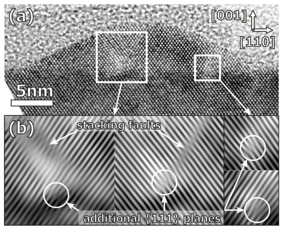
Figure 3.
(a) HRTEM image of a Si island with {113} facets and two defects marked by white squares. (b) FFT filtered images of the marked areas with the defects showing the two different sets of {111} planes. The defects are partial dislocations accompanied by stacking faults indicated by the two opposite additional {111} half-planes. Adapted from [45].
Because of the importance of the orientation of the built-in strain to the primary slip system, the compressive or tensile strained growth of SiGe on different substrate orientations like (001), (110) or (111), can lead to perfect dislocations or stacking faults [47,48]. This is especially true if SiGe is grown on complex substrates containing various facets. This occurs, for instance, during the overgrowth of large SK islands on pre-pattered substrates. Such concepts are used for example for site-controlled SK dot growth, exploiting the island strain fields as stressors, as investigated by Hrauda et al. [49,50]. Influencing the resolved shear stress by faceting substrates is also exploited to engineer dislocation nucleation centers in SiGe heterostructures. The goal of these works is to bring the misfit dislocations under control and to produce areas free of threading dislocations. This concept works quite well; for example, Gatti et al. [51] demonstrated this by employing {111} facets in the form of trenches along the [110] directions on (001) substrates as preferential nucleation centers for dislocation loops. Similar concepts are demonstrated by Grydlik et al. [52] or Bollani et al. [53], where {111} faceted pit structures are employed. Here, TEM investigations prove that the compressive strained SiGe layer on the {111} facets leads to stacking faults. These defects originate from perfect dislocations that are generated preferentially at the facets and dissociate into partials due to the above-explained mechanism. These SiGe layers on pre-structured substrates contain areas free of dislocation crosshatch and threading dislocations and are nearly coherent with the substrate. The investigation of these heterostructures with TEM was done in most cases combining conventional imaging in plan-view and HRTEM in cross-sectional geometry, giving the necessary insight to understand the occurring dislocation mechanisms.
A novel way of growing strain-free Ge on Si is the usage of deep-patterned Si-substrates, already reviewed by Montalenti et al. [54]. The basic idea is the use of internal surfaces, where misfit dislocations can end. In this way, threading dislocations at the top surface can be avoided and dislocation-free SiGe on Si can grow. This basic idea works quite well, even if due to the high dislocation density more complicated dislocation reactions can occur, leading to vertical dislocations (VDs). These VDs again end as threading dislocations at the sample surface preventing the wanted dislocation-free SiGe. A focused ion beam (FIB) cut through such a structure is displayed in Figure 4 together with a schematic model of the system indicating two VDs. The groups working on this concept were also able to develop methods of avoiding these VDs dislocations. These VDs are sessile growth dislocations; thus, they follow the growth front during epitaxy. By using growth parameters that avoid the formation of a flat topmost facet, the VDs are forced to go to the side facets of the Ge crystallites. However, to understand in the first place the dislocation reactions, dislocation characterization performed by intensive TEM investigations have been required. One complication of this geometry was that the commonly employed plan-view specimens were not applicable due to the pillar structure. Thus, next to HRTEM dislocation characterization [31,32] on cross-sectional specimens, the LACBED method became the method of choice for clarifying these types of VDs [55,56].
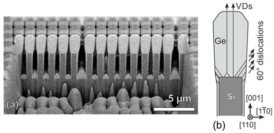
Figure 4.
(a) Focused ion beam (FIB) cut through Ge on a pillar structured substrate. (b) Schematic representation of the perfect dislocations ending on a side surface or forming vertical dislocations (VDs). Adapted from [55].
3. Large-Angle Convergent-Beam Electron Diffraction for Dislocation Analysis in SiGe
The above-mentioned examples of dislocations in SiGe heterostructures illustrate how important it is to study dislocation systems for understanding the final structures. Transmission electron microscopy has proven to be a suitable method for such investigations of dislocations in crystalline materials. Several textbooks describe in detail the concept of dislocation characterization with TEM [57]. Nevertheless, here briefly the main concepts are introduced to have the basis for the LACBED method. Even if for perfect dislocations the overall periodicity of the crystal is conserved, the crystal lattice planes are distorted around the dislocation core along the line vector, described by a displacement field R. Electrons diffracted at these lattice planes produce dislocation contrast in TEM micrographs.
The main advantage of TEM is the easy switching between imaging and diffraction mode, allowing setting certain diffraction conditions in diffraction mode at dislocation lines monitored directly in imaging mode. For a simplified interpretation of the dislocation contrast, usually the so-called two-beam condition (TBC) is applied, where only the direct beam and one diffracted beam is present in the diffraction pattern. In order to achieve this, the specimen is oriented such that only the diffraction reflection g of the desired lattice plane is excited. Either the direct or the diffracted beam is selected leading to bright- (BF) or dark-field (DF) imaging. The contrast of the dislocations in these images is governed by the exact diffraction condition, described by the excitation error sg, which is the deviation from the perfect excitation condition. For a perfect TBC, a strong dynamical contrast can be present in the images, leading to difficult interpretable contrast. Well interpretable contrast in DF images can be achieved at well-adjusted diffraction conditions with large excitation errors (sg > 0.2 nm−1), also called weak-beam dark-field (WBDF) images. In WBDF conditions, well-defined narrow dislocation lines are visible, allowing a thorough dislocation analysis [58,59]. The disadvantage of this method is that for thin TEM foils containing dislocations, strong specimen bending can be observed, which complicates the setting of an accurate value of sg. This leads to a dislocation contrast that varies strongly over larger specimen areas and makes dislocation analysis challenging.
A simpler interpretation is possible if the dislocation contrast disappears completely. This is achieved by fulfilling the invisibility criterion g·b = 0, which can be understood by a simple picture: The displacement field of an edge dislocation does not influence the lattice planes perpendicular to the line vector (g parallel to l). Therefore, a dark-field image formed with electrons diffracted from these planes (diffraction vector g) does not show any contrast of the dislocation (with a Burgers vector b), because g is perpendicular to b. The origin of the g·b term is the proportionality of the displacement field R to b. The calculation of the intensity of the diffracted electron beams, including R using the Howie–Whelan equations, lead to an additional term g·R in the phase shift of the electron waves, leading directly to the g·b = 0 condition. However, a term in the form of g·(bxl) also occurs for edge dislocations. If this term is nonzero, a dislocation contrast can be present even if g·b = 0 is satisfied. For screw dislocations, this cross-product term g·(bxl) is always zero, resulting in zero dislocation contrast for all g vectors perpendicular to l, which represent diffraction from crystal planes parallel to the line vector l. For mixed-type dislocations a combination of the above conditions applies. No contrast is visible if g·b = 0 is satisfied and additionally g·(bxl) < 0.64 is fulfilled [57]. In general, the imaging method using the invisibility criterion is best suited for dislocation analysis in SiGe alloys [60,61].
However, there are some difficulties for dislocation characterization with this imaging method. First, the diffraction condition in diffraction mode has to be adjusted, which means adjusting a proper two-beam condition for a diffraction vector g. This can be tricky, because usually a material containing dislocations is deformed, especially thin TEM foils. The deformation of the specimen can lead to the case that for each dislocation, which should be characterized, an adjustment has to be performed. This leads to frequent switching between imaging and diffraction mode and makes the measurements time consuming. Generally, three independent g·b conditions are needed to fully determine a Burgers vector in amplitude, orientation and sign. Due to geometrical reasons this is very often not possible applying different g·b = 0 conditions at one dislocation within one specimen. The combination of DF imaging exploiting g·b = 0 in plan-view geometry and HRTEM imaging with cross-sectional specimens can help to get a general three-dimensional picture of the dislocations in a sample. However, a direct method to get three independent conditions at exactly the same dislocation, without relying on difficult contrast interpretation, can be achieved with LACBED.
The LACBED method is a defocused variation of the CBED technique, which has a wide range of applications [34,62]. In classical CBED, the probe is a focused, convergent electron beam that illuminates the sample at one spot. Instead of the typical diffraction spots from parallel illumination, the diffraction reflections for Bragg diffraction vectors g = hkl are discs. A convergent probe containing different angles of incidence can be understood as the realization of different diffraction conditions in one experimental shot. The diameter of the discs is defined by the convergent angle of the probe. A perfect Bragg condition g with excitation error zero is visible in the diffraction disc g by a hkl Bragg diffraction line. A good example to visualize this is the well-known application of specimen thickness determination with CBED. In CBED patterns at a TBC, the Bragg condition is perfectly fulfilled and the hkl line is accompanied by dynamical fringes that can be analyzed for determining the specimen thickness. Thus, the intensity variation in a diffraction disk g contains the diffraction information for varying sg, which can be seen as a well-controlled diffraction map and can be used in more complex experiments for detailed symmetry, structure factor or electron density determinations for crystalline materials [63,64].
If large convergent angles are used, typically the different diffraction discs overlap and form a so-called Kossel pattern. The LACBED method now allows selecting only one diffraction disc avoiding this overlap and to take advantage of the large convergent angle. The method was first described by Tanaka et al. [65,66]. The starting point is a CBED illumination of the sample. Then the sample is displaced out of focus by the distance h above the object plane. In this way, instead of a spot, an area of the specimen is illuminated, which superimposes the diffraction information as the so-called shadow image. The beam remains focused in the object plane producing an under-focused CBED condition. In this defocused setting, all diffracted beams are focused on the object plane as shown in the sketch of the ray path in Figure 5. This allows selecting one beam with the selected area diffraction (SAD) aperture, which is placed as a virtual aperture in the image plane of the objective lens. Selecting one beam with the SAD aperture shades the others and avoids the overlap in the form of a Kossel pattern. If one selects the direct beam, a bright-field (BF)-LACBED pattern of the 000 disc is formed; if one chooses a diffracted beam, a dark-field (DF)-LACBED pattern of the respective g disc is generated. If nothing else is stated in the following text, a BF-LACBED pattern is meant.
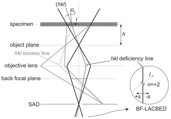
Figure 5.
Sketch of the ray diagram for a large-angle convergent-beam electron diffraction (LACBED) measurement. The specimen is displaced by the distance h out of the object plane, but the convergent beam (black) and diffracted beams (gray) remain focused in the objective plane. This allows selecting a single beam, as indicated here with the SAD aperture, avoiding the Kossel pattern and leading to a BF-LACBED pattern. The image is created in the back focal plane, represented by the circle with the hkl deficiency line and the overlaid shadow image of a dislocation, indicated by a line vector l. The splittings and the excitation error coordinate system for this hkl line are also schematically drawn.
In a BF-LACBED diffraction pattern hkl deficiency Bragg lines are visible, which are the missing intensities of electrons diffracted at the diffraction vectors g = hkl, indicated in the circle in Figure 5. The electrons diffracted by g are visible as hkl excess Bragg lines in the corresponding DF-LACBED. In a BF-LACBED pattern it is possible to monitor several different diffraction conditions at one tilt position, because several hkl deficiency Bragg diffraction lines can be present. The LACBED method is very sensitive to the smallest lattice changes [67]. This allows various applications, like determination of the elastic strain in SiGe structures [68,69,70] or, for instance, the measurement of lattice displacements in thin Ge layers or islands buried in silicon in plan-view geometry [71]. The high sensitivity to strain and lattice deformation can also be a drawback, especially if applied to complex materials like multiphase steel systems, even if it works quite well for austenitic steel grades [72]. However, exactly this high sensitivity makes this method ideally suited for dislocation characterization.
Because in the defocused LACBED setting an area is illuminated, the diffraction information is overlaid with the shadow image, the defocused image of the illuminated area. In case of a perfect crystalline Si, due to the crystal symmetries, the result is comparable to a standard CBED pattern. However, if a defect is present in the illuminated area it is visible in the shadow image. The diffraction information of the diffraction disc can be interpreted as a diffraction map of the structure in the shadow image, in which for each point of the shadow image a slightly different, but well-defined, diffraction condition is fulfilled. Moving the specimen under this illumination condition allows then to easily adjust a distinct diffraction condition for a structure in the specimen. Dislocation lines can therefore be placed in such a way that they cross several different hkl Bragg diffraction lines. This is exactly what is done for dislocation characterization if a dislocation line in the shadow image is moved to the position of a hkl line, as then the strain field of the dislocation results in n splittings of the hkl line, which is described by the g·b = n criterion. For a measurement of the Burgers vectors with LACBED, again g·b values are determined, whereas g·b = n gives easier access to the needed equations compared to the invisibility criterion, which only exploits g·b = 0. Due to the convergent angle, next to the zero order Laue zone (ZOLZ) additional hkl lines of higher order Laue zone (HOLZ) lines are accessible that contain the necessary three-dimensional information [73].
Cherns and Preston first described the contrast of dislocations in LACBED patterns in 1989 [74,75]. They found the simple criterion, called the Cherns–Preston rule, that |g·b| equals the number of splittings visible at the crossing point of a dislocation line with Burgers vector b and the Bragg line with diffraction vector g = hkl. In a simple picture, g·b < 1 means that the distortion of the lattice by the dislocation destroys the Bragg condition, thus the hkl line disappears. At g·b = 1 the distortion is exactly large enough for the Bragg condition to be again fulfilled, thus the hkl line appears again and the first splitting is built up. Therefore, for a condition g·b = n, exactly n splittings appear. A detailed discussion of the contrast in LACBED can be found in the article of Chou et al. [76], where the Cherns–Preston rules are discussed in detail. Further, a generalized many-beam dynamical computational method for the simulation of the dislocation contrast is described. It is shown that for most low atomic materials, systematic many-beam dynamical interaction does not influence the Cherns–Preston rules.
Usually specimens in the SiGe system are prepared for a line of sight along a zone axis parallel to , or , depending on the geometry of the sample. Ideal specimens’ thicknesses are in the region of 50–500nm. It is important that the specimen is not too thin, as this leads to a broadening of the hkl lines and poor quality of the splittings. A further condition for a good specimen is the flatness. Thickness changes should be negligible on a scale of the illumination area and no very strong deformations should be present. Potential preparation methods are conventional methods with dimple grinding or wedge polishing and a final thinning with Argon sputtering. In addition, FIB preparation is applicable.
Important for an efficient application of the LACBED method is the knowledge of suitable hkl lines that can be used for the analysis. As an example, a typical orientation for LACBED analyses in SiGe is shown in Figure 6, where patterns near the [110] zone axis are displayed. The simulations of the LACBED patterns in Figure 6a were performed with the JEMS software package using the Bloch wave approach. Such simulated patterns contain the dynamical and kinematical information of the hkl lines and can be used for a line selection. The main zone axis of the specimen should always be the reference point for a LACBED dislocation experiment, due to the fact that the dislocation lines are well visible near the zone axis in the direct and shadow images. It is advantageous to choose hkl lines near low-index hkl lines, which show a high dynamical contrast. Close to these lines, the dislocation lines in the shadow image will show high contrast and are best visible, simplifying to track the dislocation line positions during the adjustment of a certain diffraction condition. Nevertheless, the low-index hkl lines can show dynamical fringes, such as those visible for the 004 line in the simulated pattern of Figure 6a. Dynamical fringes lead to complex splitting patterns at intersections with dislocation lines, which are difficult to interpret. That is why low-index hkl lines are not very well suitable for the actual analysis. Instead, hkl lines with higher indices and larger extinction distances compared to the low-index ones should be used. These lines exhibit kinematical or at least quasi-kinematical behavior, such as the lines and in Figure 6a. These lines show no dynamical fringes, leading to clear splittings at dislocation line crossings and are best suited for the Burgers vector determination.
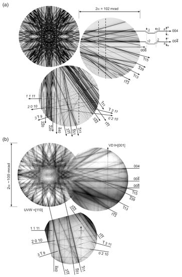
Figure 6.
(a) Simulated pattern, employed for the indexing of the experimental LACBED pattern. The sign rules are sketched at the band. (b) Experimental LACBED patterns of Ge on (001) Si recorded with a convergence angle of 50 mrad. The [110] zone axis can be seen in the top left pattern. The , and ZOLZ lines are located near the ±004 band and can be seen in the top right pattern. The dotted line with the arrow indicates where a dislocation line with line vector [001] can be present in the shadow image. The bottom pattern position can be reached by tilting along the band. Here one can find the , , and SOLZ lines suitable for an analysis of a dislocation with l = [001], again indicated with the dotted line. Adapted from [55].
The experimental patterns of Figure 6b were recorded from a thin foil prepared for [110] zone axis investigations of Ge grown on (001) Si. Such a specimen is best suited for a high-resolution investigation with the present {111} lattice fringes, used for instance for the analyses shown in Figure 3, and allowing dark-field imaging with g = , , and . Additionally, this orientation is best suited for LACBED dislocation investigations, especially if plan-view specimens are not accessible. For the g·b = n analysis with LACBED it is important that the dislocation line vectors cross the Bragg lines almost at 90°, leading to well visible splittings in the hkl lines. It is always possible to identify suitable ZOLZ hkl lines that cross any dislocation line vector close to 90°. The HOLZ lines needed for three-dimensional information are also available. HOLZ lines are ordered in a “circle” around the zona axis pole. Thus, suitable HOLZ lines, which are parallel to the selected ZOLZ lines, can be always found by a 90° turn around the zone axis. This can be accomplished experimentally by using a 90° rotated tilt axis of the specimen. Thus, for vertical dislocations with l = [001], the following lines are best suited: , , from the ZOLZ and , , , , from the second order Laue zone (SOLZ) system. The lines and the potential position of the dislocation lines in the shadow image are indicated in Figure 6b. The n values of the g·b = n condition of these lines and of perfect dislocations are displayed in Table 1. Additionally, misfit dislocations, which can originate from these perfect ones, are also included.

Table 1.
Values of g∙b for perfect 60° dislocations and their perfect products with the hkl lines presented in Figure 6. Adapted from [55]. The g vectors, used for DF imaging, can be found in the first three columns labeled as DP [110], followed by the g∙b products for the ZOLZ hkl-lines used in the LACBED analysis. The further columns are valid for the SOLZ hkl lines. The indices and distinguish between the mirror symmetrical lines on both sides of the band.
If it is previously known that only limited types of Burgers vectors are present in the material to be analyzed, very often less than three hkl line are sufficient to understand the system and the occurring dislocation reactions. Nevertheless, for a real independent three-dimensional characterization of the Burgers vectors, at least one of the hkl must be from a higher order Laue Zone containing the three-dimensional information. For an analysis, including the sign, an accurate definition of the splitting direction, sign of sg and orientation and indexing of the hkl Bragg diffraction lines is necessary. A good overview of the necessary conventions can be found in the articles of Cherns and Mornroli et al. [77,78]. It should be noted that slightly different definitions may be used by different authors, whereby a direct comparison of sign rules from different studies is often challenging. However, these rules are simplified by using fixed parameters during an experiment. This is especially true for silicon with its highly symmetric crystal system. For instance, for the analyses of the VDs from Reference [55] the displacement h of the specimen was always set positive and the right-hand rule was used to define the Burgers vectors with respect to the line vectors, which were always assumed to point into the [001] direction. To determine the sign of n first the coordinate system of sg at the hkl line has to be defined. For a pair of symmetric hkl lines, like the ±004 band in the simulation shown in Figure 6a, the following convention is used: sg is negative for a vector pointing in the direction of the symmetric line and positive for a sg vector pointing away of it. To determine now the sign of n, one follows the hkl line from the left to the right looking at the bending direction of the splittings. If the splittings bend into the direction of sg > 0, n is also positive. If the splittings bend in the other direction, n is negative. An example for a positive n splitting, following the line from the bottom to the top, is also sketched in the BF-LACBED diffraction disc of Figure 5. Various splittings at the ±004 band in Figure 6 are shown, indicating that it is also important to know the position of both symmetric lines. If one follows them from the zone axis to the right, the first splittings have different signs, even if they bend for the and line, both downwards. If in an experiment positive and negative displacements h and dislocation with various different line vectors are present, the article of Wang [79] gives general rules to determine the sign of n.
The values of the different g·b = n conditions in Table 1 were used for the analyses of the vertical dislocation (VDs) in the Ge on Si pillars [55]. Three dislocations, which are labeled 1–3, are shown in Figure 7a. The splittings for the three VDs for the ZOLZ hkl lines , and are presented in Figure 7b,c. Both images were recorded at slightly different positions. If the splittings are well visible, the actual quality depends in this case strongly on the exact position, because the strain fields of the dislocations are influenced by each other. The distance h of the specimen displacement was chosen such that the splittings of the different hkl lines are as large as possible but do not overlap.
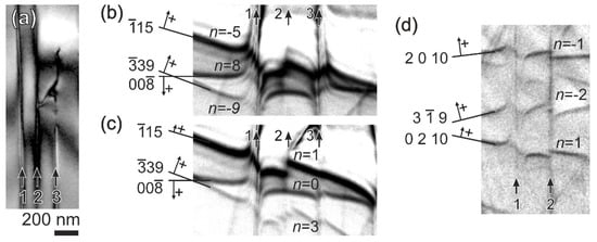
Figure 7.
(a) Three VDs with a line vector [001] and labeled 1–3. Panels (b) and (c) show the splittings of the three VDs at three different ZOLZ hkl lines. (d) Complementary measurement of dislocations #1 and #2 with SOLZ hkl lines. Adapted from [55].
It is also visible that for all hkl lines the start of the splitting is at the same position. This is the position where the strain field of the dislocation starts to influence the electron diffraction, leading to the different splitting spacing for different lines. For instance, n = −5 splittings in the line for dislocation #1 are shown in Figure 7b,c, while for the and the lines n = −9 and n = 8 splittings appear, respectively. For dislocation #3 the same behavior is observed, but with opposite signs. Dislocation #2 is different and produces n = 1, 0, and 3 splittings at the respective , and lines. Even if these are already three conditions, a full determination is not possible, because one of these indices is always a linear combination of the other two. For the full characterization, a HOLZ line index is missing, which is shown in Figure 7d. Here, for dislocation #2 n = −1, −2, and 1 splittings can be monitored. With this information, the Burgers vector of dislocation #2 can be determined as , indicating an edge dislocation. For the line defect #1 the splittings could be only read out via image processing and fits the values in Table 1 for a dislocation with the Burgers vector , which is a screw dislocation. This example shows that it is possible to determine the exact Burgers vectors of a dislocation in orientation, amplitude and sign. It can be achieved with a typical specimen for [110] zone axis investigations and LACBED, recording splittings at ZOLZ and HOLZ hkl lines. This is a large advantage compared to the method of combining plan-view specimens with cross-sectional HRTEM imaging.
Morniroli et al. [78,80] also discuss in detail how small dislocation loops can be investigated with LACBED. Analysis of dislocation loops in semiconductors larger than 100 nm can be done similar to straight dislocations [66,81], because one has the freedom to choose the size of the shadow image by the defocus parameter h. However, for small dislocation loops with less than 100 nm extension, optimized conditions are needed. Two challenges are usually present: First, the size of the shadow image of the dislocation loop is too small with respect to the diffraction pattern and the splittings are not well visible or separated. One can use a very small displacement parameter h, leading to a large magnification of the dislocation loops in the shadow image. However, a small displacement parameter leads to small distances between the direct and diffracted beams in the object plane. A separation of the direct beam from the diffracted beam to avoid the Kossel pattern is then only possible with a very small selected-area diffraction aperture. Morniroli et al. used a 2 µm diameter SAD instead of typical standard SAD with sizes of ~10 µm. The second challenge is generally strongly varying contrast of dislocation lines in the shadow image. Thus, for small loops it is difficult to keep the area of interest in the eye during tilting and adjusting to the correct diffraction condition. Morniroli solved this by marking the loop position on the specimen by small contamination spots induced by the electron beam. The work describes in detail the method to analyze small loops for an Al–Cu–Mg alloy, an austenitic steel and a boron implanted Si specimen. For the latter two materials, experimental data along with sketches of the splittings are shown in Figure 8. Different loops with and are shown, whereby for some g.b conditions n is not an integer, which lead to a more complex pattern. The shown patterns are in accordance with the LACBED splitting simulations for partial dislocations presented in the book of Tanaka et. al. [66].
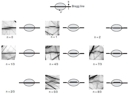
Figure 8.
Examples of experimental and schematized splittings obtained from an irradiated steel specimen and a boron-implanted Si specimen. They correspond to interstitial loops with the loop normally surrounded by a Frank partial dislocation with . Note the effect of the stacking fault with fault vector for the non-integral values of n. Reprinted with permission from Reference [78].
This also shows that LACBED can be employed to analyze the Burgers vectors of partial dislocations. Here it is important to use reflections, for which the associated stacking fault is out of contrast. Cherns and Morniroli [77] demonstrated that it is possible to analyze Shockley and Frank partial dislocations and stair-rod dislocations of type at SF intersections in Si, GaAs and CdTe. For these experiments, it is important to fulfil an additional condition: The scalar product of the R vector of the accompanying stacking fault and the chosen g should give zero or an integer, because then the SF is out of contrast and the analysis of the accompanying partial dislocations is possible. For the measurements in Si of reference [77] the used hkl lines to analyze partial and stair-rod dislocation of stacking fault on {111} planes originate from diffraction at {10 2 0}, {8 4 0}, {6 6 0}, {5 5 1}, {3 3 3}, {6 4 2} planes.
In addition, the potential of analyzing grain boundaries (GBs) and dissociated dislocations is discussed. Generally, LACBED is suited for GB analysis, which is shown by Morniroli and Cherns [82] on S3 and S9 grain boundaries in Si. In this work, a method to determine the displacement shift complete lattice vectors with LACBED is presented. Rousseau et al. [83] also employed LACBED for analyzing the structure of GBs in ultra-thin (001) Si films bonded to silicon that were analyzed by a combination of X-ray diffraction and TEM techniques. By combining the methods, it was possible to identify two kinds of dislocation networks. While a square one with screw dislocations was accommodated to the twin of the two crystals, the other linear network with dislocations of the mixed type was assigned to the tilt term of the bonding mismatch. The precision of mismatch determination of the three methods used, analysis of the periodicity of the dislocation network, LACBED measurements and X-ray diffraction, were compared. The LACBED method is generally applicable for all kinds of crystal structures. Especially for materials with similar crystal symmetries, the hkl line selection can be easily transferred from one material to another. So, a similar line selection can be used for LACBED measurements in the different semiconductor systems with a diamond or zinc blende structure. The LACBED method is also best suited for other Si-based materials with different crystal symmetries. For example, detailed LACBED investigations of dislocation structures and reactions in the more complex hexagonal crystal structure of 4H-SiC can be found in literature [84,85,86,87].
A similar principle to LACBED can be applied in direct imaging with bend contours as well. In the bend contour method, presented by Spiecker et al. [59,88,89], also direct space, and diffraction information is used. However, for this method, the images are formed in the imaging mode and overlaying bend contours, which are the representations of the hkl lines in the direct space, are used for the Burgers vector determination. Usually the LACBED method is preferred, because the TEM operator has more freedom over the experimental parameters like tilting, apertures, convergent angle and specimen defocus h. The needed variation of the diffraction condition (the excitation error) in LACBED is well determined by the convergence angle and the sample displacement h. For the bend contour method, sg is determined by the bending of the thin specimen, which cannot be influenced easily, if at all. However, Spiecker et al. showed that for plan-view samples very often a favorable bending of the specimen can be present, which leads to well defined bend contours. For the investigations large area thinned foils were used as specimens. To produce them, SiGe/Si heterostructures were polished from the backside to about ~8 µm, glued to a Cu ring and sputtered further mainly from the backside with Ar+ ions. This led to strongly bent thin foils, which can be used for the bend contour method. In this case the large advantage of the bend contour method is the very fast and reliable Burgers vector statistics, which is in most cases not possible with classical DF, WBDF, HRTEM or LACBED. The analysis with a bend contour, which is overlaid to the misfit dislocation network of a SiGe heterostructure, is depicted in Figure 9. Several dislocations are crossing the bend contour. The Cherns and Preston rule g·b = n is valid, leading to a similar analysis as in a LACBED pattern. The sign of n follows the same rules as for the LACBED method, as can be seen from the sketch in Figure 9. With the bend contour it is only possible to determine the screw component of 60° mixed type dislocations, which is done in Figure 9 for a high number of dislocations. The other components could be determined by bend contours from higher order Laue zones or effects like dislocation-induced foil buckling, described in Reference [88]. This directly shows the advantages and disadvantages of the bent contour method compared to the LACBED method. For statistics, in this example to determine the sign of the screw component for 60° dislocations, the bend contour method is more favorable. The disadvantage lies in the dependence on the sample bending and thus the lack of controllability of the excitation error. Moreover, a simple full three-dimensional characterization is only possible with the LACBED method.
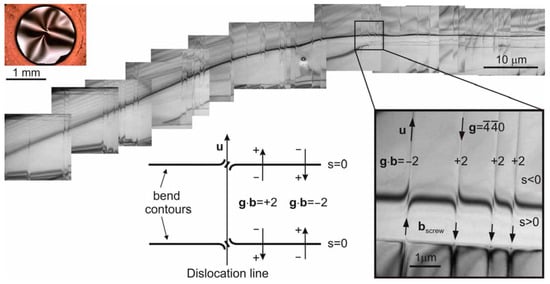
Figure 9.
Bend contour method for large-area Burgers vector analysis of misfit dislocations. Top left: Large-area plan-view thinned sample of a low-mismatched GeSi/Si (001) heterostructure. The sample shows strong bending due to coherent strain, which is only partly released by misfit dislocations. Centre: Example for the determination of the Burgers vector screw-components, bscrew, of more than 50 dislocations from the splitting of a bend contour at intersections with dislocations in a series of TEM BF images. Bottom right: Enlarged part showing the details of the splitting, the excitation error s and the deduced screw components for four dislocations. Bottom center: Diagram for evaluation of the g·b from the bend contour splitting. The same diagram is used for the evaluation of diffraction line splitting in LACBED patterns. Reprinted with permission from Reference [59].
4. Conclusions and Perspectives
TEM is a powerful method for investigating dislocations and dislocation reactions in SiGe heterostructures. The g·b = 0 criterion, applied in bright- or dark-field imaging at well-adjusted diffraction conditions, allows determining the Burgers vectors and dislocation reactions. Furthermore, HRTEM imaging allows a direct look at the atomic arrangement of the dislocation cores and interpretation with respect to strain and the dislocation displacement field. Combining these methods on plan-view and cross-sectional specimens leads to a three-dimensional picture of the dislocations and their reactions in heterostructures. On the other hand, not for all structures; for instance, for the presented SiGe on pre-patterned Si substrates, it is possible to adjust the suitable diffraction vectors g for a g·b analysis or to prepare a suitable crystallographic orientation for HRTEM imaging due to geometrical reasons.
In such cases, an alternative is the employment of the LACBED method, where the g·b = n criterion is exploited. LACBED allows the simple determination of the Burgers vectors by counting the amount of line splittings, even if together with simulations a more detailed characterization of displacement fields is possible. Due to the access to higher order Laue zone Bragg lines, fast three-dimensional characterization of Burgers vectors with amplitude and sign is possible. Important is a good choice of the used lines, of which several examples are given in this review. Alternatively, the same effect can also be used as the bending contour method, which allows achieving a better statistic.
HRTEM and LACBED are complementary techniques. HRTEM, in particular if recorded with modern aberration corrected instruments, allows direct imaging of the atomic arrangement and the dislocation displacement fields, leading to new insights in recent years. However, there are several disadvantages of HRTEM analysis. One is the difficult sample preparation, because the specimens have to be thinner compared to LACBED specimens and the general demands on specimen quality are higher. Thinner specimens are more sensitive to surface artefacts, like amorphization or implantation of atoms from the thinning process and they become more sensitive to beam damage. In the case of SiGe structures this happens above 200 keV acceleration voltage. Additionally, the specimens can deform due to built-in strain and dislocation dissociation into partials or the formation of threading dislocations to the nearby surface can occur, changing the original state drastically. For the LACBED method, thicker specimens can be employed, reducing some of the mentioned difficulties. Thus, high potential for the LACBED method is expected in the future due to the following reasons:
- (1)
- Method for non-expensive analytic standard TEMs.
- (2)
- Thicker specimens—advantages for specimen preparation.
- (3)
- Thicker specimens—less specimen artifacts.
- (4)
- Modern instruments can allow fast and automatic recording in scanning mode.
- (5)
- Software can allow automatic identification.
Especially the last two points will make LACBED more applicable. One disadvantage, which is often mentioned, is the complicated pattern with the hkl lines, which has to be indexed. However, the indexing is, with some experience, quite easy and straightforward. If one identifies the main zone axis, further indexing can be done with automatic or semiautomatic routines. Also possible is the operation of LACBED in scanning mode, a method that has been applied for CBED since the first scanning instruments were available. With modern software using machine learning, it should be possible to identify and interpret the splittings automatically.
Funding
The financial support by the Austrian Federal Ministry for Digital and Economic Affairs and the National Foundation for Research, Technology and Development in the frame of the CDL for Nanoscale Phase Transformations is gratefully acknowledged.
Acknowledgments
I would like to thank all my co-workers and colleagues who supported the TEM experiments presented here with their research. In particular, I would like to thank those responsible for providing the different material structures that I was able to investigate as well as for the sample preparation: M. Brehm, M. Glaser, M. Grydlik, G. Hesser, F. Isa, G. Isella, A. Marzegalli, L. Miglio, D. Pachinger, and F. Schäffler as well as all other involved contributors.
Conflicts of Interest
The author declares no conflict of interest.
References
- Maszara, W.P.; Goetz, G.; Caviglia, A.; McKitterick, J.B. Bonding of silicon wafers for silicon-on-insulator. J. Appl. Phys. 1988, 64, 4943–4950. [Google Scholar] [CrossRef]
- Zhou, Y.C.; Zhu, Z.H.; Crouse, D.; Lo, Y.H. Electrical properties of wafer-bonded GaAs/Si heterojunctions. Appl. Phys. Lett. 1998, 73, 2337–2339. [Google Scholar] [CrossRef]
- Liang, J.; Nishida, S.; Arai, M.; Shigekawa, N. Effects of thermal annealing process on the electrical properties of p+-Si/n-SiC heterojunctions. Appl. Phys. Lett. 2014, 104, 161604. [Google Scholar] [CrossRef]
- Rosenblad, C.; Deller, H.R.; Dommann, A.; Meyer, T.; Schroeter, P.; von Känel, H. Silicon epitaxy by low-energy plasma enhanced chemical vapor deposition. J. Vac. Sci. Technol. A Vac. Surf. Film 1998, 16, 2785–2790. [Google Scholar] [CrossRef]
- Kazior, T.E. Beyond Cmos: Heterogeneous integration of III-V devices, RF MEMS and other dissimilar materials/devices with Si CMOS to create intelligent microsystems. Philos. Trans. R. Soc. A 2014, 372, 20130105. [Google Scholar] [CrossRef]
- Kimoto, T.; Nishino, H.; Yoo, W.S.; Matsunami, H. Growth mechanism of 6H-SiC in step-controlled epitaxy. J. Appl. Phys. 1993, 73, 726–732. [Google Scholar] [CrossRef]
- Ieong, M.; Doris, B.; Kedzierski, J.; Rim, K.; Yang, M. Silicon device scaling to the sub-10-nm regime. Science 2004, 306, 2057–2060. [Google Scholar] [CrossRef]
- Wang, G.L.; Moeen, M.; Abedin, A.; Kolahdouz, M.; Luo, J.; Qin, C.L.; Zhu, H.L.; Yan, J.; Yin, H.Z.; Li, J.F.; et al. Optimization of SiGe selective epitaxy for source/drain engineering in 22 nm node complementary metal-oxide semiconductor (CMOS). J. Appl. Phys. 2013, 114, 123511. [Google Scholar] [CrossRef]
- Wirths, S.; Geiger, R.; von den Driesch, N.; Mussler, G.; Stoica, T.; Mantl, S.; Ikonic, Z.; Luysberg, M.; Chiussi, S.; Hartmann, J.M.; et al. Lasing in direct-bandgap GeSn alloy grown on Si. Nat. Photonics 2015, 9, 88–92. [Google Scholar] [CrossRef]
- Groiss, H.; Glaser, M.; Schatzl, M.; Brehm, M.; Gerthsen, D.; Roth, D.; Bauer, P.; Schäffler, F. Free-running Sn precipitates: An efficient phase separation mechanism for metastable Ge1−xSnx epilayers. Sci. Rep. 2017, 7, 16144. [Google Scholar] [CrossRef]
- Michel, J.; Liu, J.; Kimerling, L.C. High-performance Ge-on-Si photodetectors. Nat. Photonics 2010, 4, 527–534. [Google Scholar] [CrossRef]
- Camacho-Aguilera, R.E.; Cai, Y.; Patel, N.; Bessette, J.T.; Romagnoli, M.; Kimerling, L.C.; Michel, J. An electrically pumped germanium laser. Opt. Express 2012, 20, 11316. [Google Scholar] [CrossRef] [PubMed]
- Schatzl, M.; Hackl, F.; Glaser, M.; Rauter, P.; Brehm, M.; Spindlberger, L.; Simbula, A.; Galli, M.; Fromherz, T.; Schäffler, F. Enhanced Telecom Emission from Single Group-IV Quantum Dots by Precise CMOS-Compatible Positioning in Photonic Crystal Cavities. ACS Photonics 2017, 4, 665–673. [Google Scholar] [CrossRef] [PubMed]
- Grydlik, M.; Brehm, M.; Hackl, F.; Groiss, H.; Fromherz, T.; Schäffler, F.; Bauer, G. Inverted Ge islands in {111} faceted Si pits—A novel approach towards SiGe islands with higher aspect ratio. New J. Phys. 2010, 12, 063002. [Google Scholar] [CrossRef]
- Zhang, J.J.; Montalenti, F.; Rastelli, A.; Hrauda, N.; Scopece, D.; Groiss, H.; Stangl, J.; Pezzoli, F.; Schäffler, F.; Schmidt, O.G.; et al. Collective shape oscillations of sige islands on pit-patterned Si(001) substrates: A coherent-growth strategy enabled by self-regulated intermixing. Phys. Rev. Lett. 2010, 105, 166102. [Google Scholar] [CrossRef]
- Thewalt, M.L.W.; Harrison, D.A.; Reinhart, C.F.; Wolk, J.A.; Lafontaine, H. Type II band alignment in Si1−xGex/Si(001) quantum wells: The ubiquitous type I luminescence results from band bending. Phys. Rev. Lett. 1997, 79, 269–272. [Google Scholar] [CrossRef]
- Grydlik, M.; Hackl, F.; Groiss, H.; Glaser, M.; Halilovic, A.; Fromherz, T.; Jantsch, W.; Schäffler, F.; Brehm, M. Lasing from glassy Ge quantum dots in crystalline Si. ACS Photonics 2016, 3, 298–303. [Google Scholar] [CrossRef]
- Groiss, H.; Spindlberger, L.; Oberhumer, P.; Schäffler, F.; Fromherz, T.; Grydlik, M.; Brehm, M. Photoluminescence enhancement through vertical stacking of defect-engineered Ge on Si quantum dots. Semicond. Sci. Technol. 2017, 32, 02LT01. [Google Scholar] [CrossRef]
- Schmidt, O.G.; Eberl, K. Self-assembled Ge/Si dots for faster field-effect transistors. IEEE Trans. Electron Devices 2001, 48, 1175–1179. [Google Scholar] [CrossRef]
- Thompson, S.E.; Armstrong, M.; Auth, C.; Cea, S.; Chau, R.; Glass, G.; Hoffman, T.; Klaus, J.; Ma, Z.; Mcintyre, B.; et al. A logic nanotechnology featuring strained-silicon. IEEE Electron Device Lett. 2004, 25, 191–193. [Google Scholar] [CrossRef]
- Jovanovic, V.; Biasotto, C.; Nanver, L.K.; Moers, J.; Grutzmacher, D.; Gerharz, J.; Mussler, G.; Van Der Cingel, J.; Zhang, J.J.; Bauer, G.; et al. N-channel MOSFETs fabricated on SiGe dots for strain-enhanced mobility. IEEE Electron Device Lett. 2010, 31, 1083–1085. [Google Scholar] [CrossRef]
- Pernot, G.; Stoffel, M.; Savic, I.; Pezzoli, F.; Chen, P.; Savelli, G.; Jacquot, A.; Schumann, J.; Denker, U.; Mönch, I.; et al. Precise control of thermal conductivity at the nanoscale through individual phonon-scattering barriers. Nat. Mater. 2010, 9, 491–495. [Google Scholar] [CrossRef] [PubMed]
- Chang, H.T.; Wang, S.Y.; Lee, S.W. Designer Ge/Si composite quantum dots with enhanced thermoelectric properties. Nanoscale 2014, 6, 3593–3598. [Google Scholar] [CrossRef] [PubMed]
- Thumfart, L.; Carrete, J.; Vermeersch, B.; Ye, N.; Truglas, T.; Feser, J.; Groiss, H.; Mingo, N.; Rastelli, A. Thermal transport through Ge-rich Ge/Si superlattices grown on Ge(0 0 1). J. Phys. D Appl. Phys. 2018, 51, 014001. [Google Scholar] [CrossRef]
- Hӱtch, M.J.; Putaux, J.L.; Thibault, J. Stress and strain around grain-boundary dislocations measured by high-resolution electron microscopy. Philos. Mag. 2006, 86, 4641–4656. [Google Scholar] [CrossRef]
- Bolkhovityanov, Y.B.; Deryabin, A.S.; Gutakovskii, A.K.; Sokolov, L.V. Mechanism of induced nucleation of misfit dislocations in the Ge-on-Si(001) system and its role in the formation of the core structure of edge misfit dislocations. Acta Mater. 2013, 61, 617–621. [Google Scholar] [CrossRef]
- Bolkhovityanov, Y.B.; Gutakovskii, A.K.; Deryabin, A.S.; Sokolov, L.V. Specific features of plastic relaxation of a metastable GexSi1−x layer buried between a silicon substrate and a relaxed germanium layer. Phys. Solid State 2014, 56, 247–253. [Google Scholar] [CrossRef]
- Bolkhovityanov, Y.B.; Gutakovskii, A.K.; Deryabin, A.S.; Sokolov, L.V. Experimental observation of motion of edge dislocations in Ge/GexSi1−x/Si(001) (x = 0.2–0.6) heterostructures. J. Exp. Theor. Phys. 2016, 123, 832–837. [Google Scholar] [CrossRef]
- Bolkhovityanov, Y.B.; Deryabin, A.S.; Gutakovskii, A.K.; Sokolov, L.V. Unzipping and movement of Lomer-type edge dislocations in Ge/GeSi/Si(001) heterostructures. J. Cryst. Growth 2018, 483, 265–268. [Google Scholar] [CrossRef]
- Dou, W.; Benamara, M.; Mosleh, A.; Margetis, J.; Grant, P.; Zhou, Y.; Al-Kabi, S.; Du, W.; Tolle, J.; Li, B.; et al. Investigation of GeSn Strain Relaxation and Spontaneous Composition Gradient for Low-Defect and High-Sn Alloy Growth. Sci. Rep. 2018, 8, 5640. [Google Scholar] [CrossRef]
- Arroyo Rojas Dasilva, Y.; Rossell, M.D.; Keller, D.; Gröning, P.; Isa, F.; Kreiliger, T.; Von Känel, H.; Isella, G.; Erni, R. Analysis of edge threading dislocations b = 1/2 <110> in three dimensional Ge crystals grown on (001)-Si substrates. Appl. Phys. Lett. 2015, 107, 093501. [Google Scholar] [CrossRef]
- Arroyo Rojas Dasilva, Y.; Rossell, M.D.; Isa, F.; Erni, R.; Isella, G.; von Känel, H.; Gröning, P. Strain relaxation in epitaxial Ge crystals grown on patterned Si(001) substrates. Scr. Mater. 2017, 127, 169–172. [Google Scholar] [CrossRef]
- Arroyo Rojas Dasilva, Y.; Isa, F.; Isella, G.; Erni, R.; von Känel, H.; Gröning, P.; Rossell, M.D. Effect of thermal annealing on the interface quality of Ge/Si heterostructures. Scr. Mater. 2019, 170, 52–56. [Google Scholar] [CrossRef]
- Tanaka, M.; Tsuda, K. Convergent-beam electron diffraction. Microscopy 2011, 60, 245–267. [Google Scholar] [CrossRef]
- Stranski, I.N.; Krastanow, L. Berichtigung zur Arbeit—“Zur Theorie der orientierten Ausscheidung von Ionenkristallen aufeinander”. Mon. Chem. 1939, 72, 76. [Google Scholar] [CrossRef]
- Brehm, M.; Groiss, H.; Bauer, G.; Gerthsen, D.; Clarke, R.; Paltiel, Y.; Yacoby, Y. Atomic structure and composition distribution in wetting layers and islands of germanium grown on silicon (001) substrates. Nanotechnology 2015, 26, 485702. [Google Scholar] [CrossRef][Green Version]
- Rosenauer, A.; Remmele, T.; Gerthsen, D.; Tillmann, K.; Förster, A. Atomic scale strain measurements by the digital analysis of transmission electron microscopic lattice images. Optik 1997, 105, 99–107. [Google Scholar]
- Hӱtch, M.J.; Snoeck, E.; Kilaas, R. Quantitative measurement of displacement and strain fields from HREM micrographs. Ultramicroscopy 1998, 74, 131–146. [Google Scholar] [CrossRef]
- Marée, P.M.J.; Barbour, J.C.; Van Der Veen, J.F.; Kavanagh, K.L.; Bulle-Lieuwma, C.W.T.; Viegers, M.P.A. Generation of misfit dislocations in semiconductors. J. Appl. Phys. 1987, 62, 4413–4420. [Google Scholar] [CrossRef]
- Wegscheider, W.; Eberl, K.; Abstreiter, G.; Cerva, H.; Oppolzer, H. Novel relaxation process in strained Si/Ge superlattices grown on Ge (001). Appl. Phys. Lett. 1990, 57, 1496–1498. [Google Scholar] [CrossRef]
- Kvam, E.P.; Hull, R. Surface orientation and stacking fault generation in strained epitaxial growth. J. Appl. Phys. 1993, 73, 7407–7411. [Google Scholar] [CrossRef]
- Liu, P.; Zhang, Y.W.; Fox, B.; Lu, C. Molecular dynamics study of dislocation formation in a [001] face-centered-cubic epitaxial island under tensile stress. Appl. Phys. Lett. 2004, 84, 714–716. [Google Scholar] [CrossRef]
- Bedell, S.W.; Reznicek, A.; Yang, B.; Hovel, H.J.; Ott, J.A.; Fogel, K.; Domenicucci, A.G.; Sadana, D.K. Development of stacking faults in strained silicon layers. In Proceedings of the IEEE International SOI Conference, Honolulu, HI, USA, 3–6 October 2005; pp. 144–145. [Google Scholar]
- Hartmann, J.M.; Abbadie, A.; Rouchon, D.; Barnes, J.P.; Mermoux, M.; Billon, T. Structural properties of tensile-strained Si layers grown on Si1−xGex virtual substrates (x = 0.2, 0.3, 0.4 and 0.5). Thin Solid Films 2008, 516, 4238–4246. [Google Scholar] [CrossRef]
- Pachinger, D.; Groiss, H.; Teuchtmann, M.; Hesser, G.; Schäffler, F. Surfactant-mediated Si quantum dot formation on Ge(001). Appl. Phys. Lett. 2011, 98, 223104. [Google Scholar] [CrossRef]
- Pachinger, D.; Groiss, H.; Lichtenberger, H.; Stangl, J.; Hesser, G.; Schäffler, F. Stranski-Krastanow growth of tensile strained Si islands on Ge (001). Appl. Phys. Lett. 2007, 91, 233106. [Google Scholar] [CrossRef]
- Lee, M.L.; Antoniadis, D.A.; Fitzgerald, E.A. Challenges in epitaxial growth of SiGe buffers on Si (111), (110), and (112). Thin Solid Films 2006, 508, 136–139. [Google Scholar] [CrossRef]
- Norris, D.J.; Myronov, M.; Leadley, D.R.; Walther, T. Comparison of cross-sectional transmission electron microscope studies of thin germanium epilayers grown on differently oriented silicon wafers. J. Microsc. 2017, 268, 288–297. [Google Scholar] [CrossRef]
- Hrauda, N.; Zhang, J.J.; Groiss, H.; Gerharz, J.C.; Etzelstorfer, T.; Stangl, J.; Holý, V.; Deiter, C.; Seeck, O.H.; Bauer, G. Closely spaced SiGe barns as stressor structures for strain-enhancement in silicon. Appl. Phys. Lett. 2013, 102, 032109. [Google Scholar] [CrossRef]
- Hrauda, N.; Zhang, J.J.; Groiss, H.; Etzelstorfer, T.; Holý, V.; Bauer, G.; Deiter, C.; Seeck, O.H.; Stangl, J. Strain relief and shape oscillations in site-controlled coherent SiGe islands. Nanotechnology 2013, 24, 335707. [Google Scholar] [CrossRef]
- Gatti, R.; Boioli, F.; Grydlik, M.; Brehm, M.; Groiss, H.; Glaser, M.; Montalenti, F.; Fromherz, T.; Schäffler, F.; Miglio, L. Dislocation engineering in SiGe heteroepitaxial films on patterned Si (001) substrates. Appl. Phys. Lett. 2011, 98, 121908. [Google Scholar] [CrossRef]
- Grydlik, M.; Boioli, F.; Groiss, H.; Gatti, R.; Brehm, M.; Montalenti, F.; Devincre, B.; Schäffler, F.; Miglio, L. Misfit dislocation gettering by substrate pit-patterning in SiGe films on Si(001). Appl. Phys. Lett. 2012, 101, 013119. [Google Scholar] [CrossRef]
- Bollani, M.; Chrastina, D.; Ruggeri, R.; Nicotra, G.; Gagliano, L.; Bonera, E.; Mondiali, V.; Marzegalli, A.; Montalenti, F.; Spinella, C.; et al. Anisotropic extended misfit dislocations in overcritical SiGe films by local substrate patterning. Nanotechnology 2016, 27, 425301. [Google Scholar] [CrossRef] [PubMed]
- Montalenti, F.; Rovaris, F.; Bergamaschini, R.; Miglio, L.; Salvalaglio, M.; Isella, G.; Isa, F.; von Känel, H. Dislocation-free SiGe/Si heterostructures. Crystals 2018, 8, 257. [Google Scholar] [CrossRef]
- Groiss, H.; Glaser, M.; Marzegalli, A.; Isa, F.; Isella, G.; Miglio, L.; Schäffler, F. Burgers Vector Analysis of Vertical Dislocations in Ge Crystals by Large-Angle Convergent Beam Electron Diffraction. Microsc. Microanal. 2015, 21, 637–645. [Google Scholar] [CrossRef] [PubMed]
- Marzegalli, A.; Isa, F.; Groiss, H.; Müller, E.; Falub, C.V.; Taboada, A.G.; Niedermann, P.; Isella, G.; Schäffler, F.; Montalenti, F.; et al. Unexpected dominance of vertical dislocations in high-misfit Ge/Si(001) films and their elimination by deep substrate patterning. Adv. Mater. 2013, 25, 4408–4412. [Google Scholar] [CrossRef]
- Williams, D.W.; Carter, C.B. Transmission Electron Microscopy, 2nd ed.; Springer Science+Business Media: New York, NY, USA, 2009; pp. 441–461. [Google Scholar]
- Ishida, Y.; Ishida, H.; Kohra, K.; Ichinose, H.; Ichinose, H. Determination of the Burgers vector of a dislocation by weak-beam imaging in a HVEM. Philos. Mag. A 1980, 42, 453–462. [Google Scholar] [CrossRef]
- Spiecker, E. Novel TEM methods for large-area analysis of misfit dislocation networks in semiconductor heterostructures. Philos. Mag. 2006, 86, 4941–4963. [Google Scholar] [CrossRef]
- Stenkamp, D.; Jäger, W. Dislocations and their dissociation in SixGe1−x alloys. Philos. Mag. A 1992, 65, 1369–1382. [Google Scholar] [CrossRef]
- Bonnet, R.; Loubradou, M.; Youssef, S.; Rouvière, J.L.; Fournel, F. Alternate dissociation of the screw dislocations in a (001) buried small-angle twist boundary in silicon. Philos. Mag. 2009, 89, 413–434. [Google Scholar] [CrossRef]
- Vijayalakshmi, M.; Saroja, S.; Mythili, R. Convergent beam electron diffraction—A novel technique for materials characterisation at sub-microscopic levels. Sadhana 2003, 28, 763–782. [Google Scholar] [CrossRef]
- Tsuda, K.; Tanaka, M. Refinement of crystal structural parameters using two-dimensional energy-filtered CBED patterns. Acta Cryst. 1999, 55, 939–954. [Google Scholar] [CrossRef] [PubMed]
- Ogata, Y.; Tsuda, K.; Tanaka, M. Determination of the electrostatic potential and electron density of silicon using convergent-beam electron diffraction. Acta Crystallogr. Sect. A Found. Crystallogr. 2008, 64, 587–597. [Google Scholar] [CrossRef] [PubMed]
- Tanaka, M.; Saito, R.; Ueno, K.; Harada, Y. Large-Angle Convergent-Beam Electron Diffraction. J. Electron Microsc. 1980, 29, 408–412. [Google Scholar]
- Tanaka, M.; Terauchi, M.; Kaneyama, T. Convergent-Beam Electron Diffraction II; JEOL Ltd.: Akishima, Tokyo, Japan, 1988. [Google Scholar]
- Morniroli, J.P. CBED and LACBED characterization of crystal defects. J. Microsc. 2006, 223, 240–245. [Google Scholar] [CrossRef] [PubMed]
- Duan, X.F.; Cherns, D.; Steeds, J.W. Effects of elastic relaxation on large-angle convergent-beam electron diffraction from cross-sectional specimens of GexSi1−x/Si strained-layer superlattices. Philos. Mag. A 1994, 70, 1091–1105. [Google Scholar] [CrossRef]
- Cherns, D.; Touaitia, R.; Preston, A.R.; Rossouw, C.J.; Houghton, D.C. Convergent beam electron diffraction studies of strain in Si/SiGe superlattices. Philos. Mag. A 1991, 64, 597–612. [Google Scholar] [CrossRef]
- Rossouw, C.J.; Spellward, P.; Perovic, D.D.; Cherns, D. Dynamical zone-axis electron diffraction contrast of boron-doped Si multilayers. Philos. Mag. A 1994, 69, 255–265. [Google Scholar] [CrossRef]
- Cherns, D.; Hovsepian, A.; Jäger, W. Profiling Ge islands in Si by large angle convergent beam electron diffraction. J. Electron Microsc. 1998, 47, 211–215. [Google Scholar] [CrossRef]
- Kürnsteiner, P.; Commenda, C.; Arenholz, E.; Samek, L.; Stifter, D.; Groiss, H. Investigation of nanoscale twinning in an advanced high manganese twinning-induced plasticity steel. Materialia 2018, 1, 70–77. [Google Scholar] [CrossRef]
- Carpenter, R.W.; Spence, J.C.H. Three-dimensional strain-field information in convergent-beam electron diffraction patterns. Acta Crystallogr. A 1982, 38, 55–61. [Google Scholar] [CrossRef]
- Cherns, D.; Preston, A.R. Convergent beam diffraction studies of crystal effects. In Proceedings of the 11th International Congress on Electron Microscopy, Kyoto, Japan, 31 August–7 September 1986; Imura, T., Marusa, S., Suzuki, T., Eds.; The Japanese Society of Electron Microscopy: Tokyo, Japan, 1986; Volume 1, p. 721. [Google Scholar]
- Cherns, D.; Preston, A.R. Convergent beam diffraction studies of interfaces, defects, and multilayers. J. Electron Microsc. Tech. 1989, 13, 111–122. [Google Scholar] [CrossRef] [PubMed]
- Chou, C.T.; Preston, A.R.; Steeds, J.W. Dislocation contrast in large angle convergent-beam electron diffraction patterns. Philos. Mag. A 1992, 65, 863–888. [Google Scholar] [CrossRef]
- Cherns, D.; Morniroli, J.P. Analysis of partial and stair-rod dislocations by large angle convergent beam electron diffraction. Ultramicroscopy 1994, 53, 167–180. [Google Scholar] [CrossRef]
- Morniroli, J.P.; Marceau, R.K.W.; Ringer, S.P.; Boulanger, L. LACBED characterization of dislocation loops. Philos. Mag. 2006, 86, 4883–4900. [Google Scholar] [CrossRef]
- Wang, R. Defocus convergent beam electron diffraction determination of Burgers vectors of dislocations in quasicrystals. Micron 2000, 31, 475–486. [Google Scholar] [CrossRef]
- Morniroli, J.P.; Marceau, R.K.W.; Ringer, S.P. New developments in the characterization of dislocation loops from LACBED patterns. J. Microsc. 2006, 223, 246–248. [Google Scholar] [CrossRef]
- Jäger, C.; Spiecker, E.; Morniroli, J.P.; Jäger, W. Analysis of dislocation loops by means of large-angle convergent beam electron diffraction. J. Phys. Condens. Matter 2002, 14, 12777–12782. [Google Scholar] [CrossRef]
- Morniroli, J.P.; Cherns, D. Analysis of grain boundary dislocations by large angle convergent beam electron diffraction. Ultramicroscopy 1996, 62, 53–63. [Google Scholar] [CrossRef]
- Rousseau, K.; Eymery, J.; Fournel, F.; Morniroli, J.P.; Rouviere, J.L. (001) Silicon surfacial grain boundaries obtained by direct wafer bonding process: Accurate control of the structure before bonding. Philos. Mag. 2005, 85, 2415–2448. [Google Scholar] [CrossRef]
- Texier, M.; Regula, G.; Lancin, M.; Pichaud, B. LACBED study of extended defects in 4H-SiC. Philos. Mag. Lett. 2006, 86, 529–537. [Google Scholar] [CrossRef]
- Onda, S.; Watanabe, H.; Kito, Y.; Kondo, H.; Uehigashi, H.; Hosokawa, N.; Hisada, Y.; Shiraishi, K.; Saka, H. Transmission electron microscope study of a threading dislocation with and its effect on leakage in a 4H-SiC MOSFET. Philos. Mag. Lett. 2013, 93, 439–447. [Google Scholar] [CrossRef]
- Onda, S.; Watanabe, H.; Okamoto, T.I.; Kondo, H.; Uehigashi, H.; Saka, H. Threading dislocation with b=c+2a in 4H-SiC as determined by LACBED. Philos. Mag. Lett. 2015, 95, 489–495. [Google Scholar] [CrossRef]
- Hadorn, J.P.; Tanuma, R.; Kamata, I.; Tsuchida, H. Direct evaluation of threading dislocations in 4H-SiC through large-angle convergent beam electron diffraction. Philos. Mag. 2019. [Google Scholar] [CrossRef]
- Spiecker, E.; Jäger, W. Burgers vector analysis of large area misfit dislocation arrays from bend contour contrast in transmission electron microscope images. J. Phys. Condens. Matter 2002, 14, 12767–12776. [Google Scholar] [CrossRef]
- Spiecker, E.; Schöne, J.; Rajagopalan, S.; Jäger, W. Novel TEM method for large-area analysis of misfit dislocation networks in semiconductor heterostructures. In Microscopy of Semiconducting Materials; Springer: Berlin/Heidelberg, Germany, 2006; Volume 86, pp. 117–130. [Google Scholar]


© 2019 by the author. Licensee MDPI, Basel, Switzerland. This article is an open access article distributed under the terms and conditions of the Creative Commons Attribution (CC BY) license (http://creativecommons.org/licenses/by/4.0/).