Article

On the Study of Dislocation Density in MBE GaSb-Based Structures

1
Sieć Badawcza Łukasiewicz-Instytut Mikroelektroniki i Fotoniki, al. Lotników 32/46, 02-668 Warsaw, Poland
2
Institute of Physics Polish Academy of Science, al. Lotników 32/46, 02-668 Warsaw, Poland
*
Author to whom correspondence should be addressed.
Crystals 2020, 10(12), 1074; https://doi.org/10.3390/cryst10121074
Submission received: 3 November 2020 / Revised: 20 November 2020 / Accepted: 23 November 2020 / Published: 25 November 2020

Abstract

:
The results of the study on threading dislocation density (TDD) in homo- and heteroepitaxial GaSb-based structures (metamorphic layers, material grown by applying interfacial misfit array (IMF) and complex structures) deposited using molecular beam epitaxy are presented. Three measurement techniques were considered: high-resolution x-ray diffraction (HRXRD), etch pit density (EPD), and counting tapers on images obtained using atomic force microscopy (AFM). Additionally, high-resolution transmission electron microscopy (HRTEM) was used for selected samples. The density of dislocations determined using these methods varied, e.g., for IMF-GaSb/GaAs sample, were 6.5 × 108 cm−2, 2.2 × 106 cm−2, and 4.1 × 107 cm−2 obtained using the HRXRD, EPD, and AFM techniques, respectively. Thus, the value of TDD should be provided together with information about the measurement method. Nevertheless, the absolute value of TDD is not as essential as the credibility of the technique used for optimizing material growth. By testing material groups with known parameters, we established which techniques can be used for examining the dislocation density in GaSb-based structures.

1. Introduction

The performance of optoelectronic devices is, among other things, affected by the presence of defects in semiconductor structures, e.g., point (antisites and interstitials) and extended (dislocations) ones. The latter are formed mainly in the lattice-mismatched heterostructures. They can shunt p-n junctions [1] as well as reduce overall efficiency due to carrier scattering on the distortions around the dislocation cores [2,3]. The carrier scattering occurs in photodetectors fabricated using heterostructures grown on GaSb-buffered GaAs substrates. The large lattice mismatch of about 7.8% between GaSb epilayer and GaAs substrate leads to relaxation of the lattice strain by the generation of 60° misfit dislocations. These can propagate through the entire material structure, reaching a density in the order of 109 cm−2 [4]. Interfacial misfit (IMF) array is most frequently used for reducing the dislocation density in epitaxially grown materials [5,6]. This technique allows for relieving the strain energy by generation of 90° periodic misfit dislocations at the GaSb/GaAs interface, thus decreasing the threading dislocation density (TDD) [7]. According to Huang et al., the dislocation density (DD) can be reduced by up to four orders of magnitude to about 7 × 105 cm−2 using IMF [5,8]. Optimization of the growth of complex lattice-mismatched heterostructures requires a fast, simple, and reliable technique for estimation of dislocation density. The absolute value of TDD is not as essential as the credibility of the method used for its determination. There are three commonly used approaches, namely counting the dislocation lines on the plan-view and/or cross-sectional images obtained by the transmission electron microscopy (TEM) [9,10], calculation of the dislocation density based on the rocking curves measured at the appropriate reflections using the high-resolution x-ray diffraction method (HRXRD) [11], and counting of the etched pits on the material surface observed using scanning electron microscopy (SEM) [12]. The approaches based on TEM observations and HRXRD measurements have some limitations. TEM analysis requires time-consuming sample preparation. Furthermore, the scanned area is usually limited to a few square micrometres, which becomes problematic when the dislocation density is smaller than 106 cm−2 [12]. There is a risk of dislocations being omitted and/or not detected during the measurement. The HRXRD-based approach allows one to determine dislocation density distributed throughout the entire sample, but it is only useful when DD is within 105 ÷ 109 cm−2 [13]. In comparison with the aforementioned methods, the chemical etching of pits on the semiconductor surface has no limitations related to the sample size. Its main disadvantage is that it only accounts for dislocations which reach the sample surface and produce etch pits. There is also a risk of pits merging if a layer with a high dislocation density is etched for too long. However, this problem can be solved by adjusting the etching rate. Many solutions are used for revealing dislocation pits in bulk materials. Some of them can be applied to more than one crystallographic plane. The covalent bonds in III–V compounds impose a requirement for combination of the oxidizing agent (H2O2, HNO3, and Fe3+) and the complexing agent (HCl, H2SO4, and HF) to form stable ions in the etchant [14,15,16,17,18]. Solutions used for revealing dislocation pits on the surface of (100) GaSb bulk are based on H2O2 as an oxidizing agent [15,16]. The most commonly used complexing agent is HCl [15,16,17], while another report suggests H2SO4 [18]. However, these are intended for bulk crystals. The etch pits on the surface of the epitaxial layers are smaller in comparison with the ones revealed on the bulk material; thus, they need to be observed under a scanning electron microscope rather than an optical one. Different values of DD are expected to be obtained using the aforementioned methods due to different underlying physical phenomena. Simultaneously, the choice of the most appropriate approach for a specific material is not obvious.
The main aim of our work is to choose the most suitable method for studying threading dislocation density in GaSb-based epitaxial materials. For this purpose, we carried out a comparative study of DD for three groups of materials: homoepitaxial GaSb, heteroepitaxial metamorphic, and IMF-GaSb structures deposited on GaAs substrates, as well as complex GaSb-based heterostructures. Samples in each group were selected so that the relations between them were known with respect to the dislocation density. We applied different approaches based on HRXRD measurements, pit etching, and atomic force microscopy (AFM). The last one may be used for determining DD in a GaSb/GaAs system grown in the spiral mode. This approach assumes that each spiral refers on average to two dislocations with a screw component of the Burgers vector [19]. A summary of TDD results obtained using these three methods is given. To the best of our knowledge, such an analysis has not been presented to date. This data allowed us to conclude the appropriateness of using one or more of the considered methods for determining the dislocation density in GaSb-based materials. It follows that the information on TDD should be provided together with the information about the measurement method.

2. Experiments

The structures deposited on GaSb and GaAs substrates using molecular beam epitaxy (MBE) were the object of the experiment. The summary of the three groups of material systems that were investigated is given in Table 1. The parameters used during the growth of homoepitaxial, metamorphic, and IMF GaSb materials as well as superlattices (SL) were described in Reference [7]. The growth conditions for AlSb and Al0.5Ga0.5As0.05Sb0.95 materials are given in Reference [20]. Briefly, the growth rates were approximately 0.5 ML/s and 1.0 ML/s; growth temperature was approximately 520 °C; and beam equivalent pressure for group V and III elements (V/III) were 2.3, 2.0, and 2.9 for GaSb, AlSb, and Al0.5Ga0.5As0.05Sb0.95, respectively. V/III for thin IMF-GaSb layers (#013, #014, and #015) varied and are listed in Table 1. The low-temperature (LT) AlSb interlayers were grown at about 480 °C. The Al-containing layers were capped by a 20-nm GaSb layer for protection against oxidation.
Three main approaches based on HRXRD measurements, etch pit density (EPD), and AFM observations were used for evaluating TDD in the aforementioned structures. The samples were prepared adequately to the requirements of each technique. The HRXRD measurements were carried out on samples the size of the quarter of the two-inch substrate using a high-resolution PANalytical X’Pert PRO MRD diffractometer before cutting; 5 × 5 mm samples of GaSb material were used for etching and AFM observations. Furthermore, in the case of the EPD approach, each sample was first degreased in hot acetone followed by 2-propanol and rinsed in deionized water (DI H2O). Subsequently, samples were chemically etched, rinsed with DI water, and dried under a gaseous N2 stream.
The HRXRD approach is based on broadening of the rocking curve (RC) observed in the epitaxial structures with high dislocation density. In Reference [13], a linear dependence between β2 and tan2θ was shown:
β 2 = K α + K ε tan 2 θ ,
where β is the full width at half maximum of rocking curves measured for different reflections, θ is the Bragg angle, and Kα and Kɛ are the intercept and the slope, respectively. Kα and Kɛ coefficients are then used for calculating the dislocation density from two independent equations:
D A = K α 4.36   b 2     angular   broadening ,
D S = K ε 0.09   b 2 | ln ( 2 × 10 7 cm D S ) |     strain   broadening ,
where b is the Burgers vector. The angular broadening is related to the rotation of the crystal lattice by the dislocations, while the strain broadening is caused by lattice strain close to dislocations. Based on these two equations, the same values of dislocation density were obtained.
The main issue in revealing dislocation etch pits was proper adjustment of the etching rate to obtain the highest possible selectivity between the etching of pits and the thin epitaxial film. In Table 2, the etchants chosen for detailed examination are listed.
The 20% KOH solution (I) is a well-known etchant for revealing dislocation pits in (100) GaAs bulk crystal [21]. It was also used for estimating the dislocation density of GaSb/GaAs heteroepitaxial films with IMF similar to ours [5]. The investigated IMF-GaSb samples were etched in this solution at both room temperature (RT) and 80 °C for 30 min. Etchants II and IV were developed for etching pits in bulk GaSb crystal. For solution II, the highest etching rate (150–180 nm/s) of all considered solutions was observed. Etchant III is a modification of the second one. It is composed of H2O2–HCl–H2O and was used for estimating the EPD of the (100) GaSb buffer layer on a GaAs substrate [22]. The etching rate for this solution was reduced by diluting it with DI water. Samples were etched at room temperature and 70 °C as proposed in Reference [17] for a bulk crystal. The etching rate at 70 °C decreased slightly to about 135 nm/s in comparison to the etchant II. Decreasing temperature to RT resulted in prolongation of the etching time to 20 min and reduction of the etching rate to about 2.0 nm/s.
The last solution (V) was adapted from investigations of the {111} surfaces of the III-V compounds [23]. It was shown that this solution is also very effective in revealing dislocation etch pits on (100) plane in GaSb bulk crystal [24]. It was prepared by dissolving 21.6 g of FeCl3 in 20 mL DI H2O and supplemented to a volume of 1000 mL with concentrated HCl (35–37%). It was observed that this solution acted effectively at an elevated temperature of 40 °C, at which the etching rate was about 15 nm/s. The samples were etched for 1 min without stirring. Adjustment of the etching time to the layer thickness was crucial for revealing etch pits using this solution. It was easy to over-etch the pits, making them difficult to identify or not revealed at all. The etching time was chosen experimentally, and it varied for samples with different thicknesses. After the etching, sample surfaces were observed using an optical microscope and the etch pit density was evaluated using SEM images (tilted by 57°).
Topography images were obtained by the means of atomic force microscopy. The measurements were carried out in ambient conditions using Digital Instrument (Santa Barbara, CA, USA) Nanoscope IIIa (currently Bruker), controlled by Nanoscope 4.42 software. The microscope with mounted Olympus microcantilever (OMCL-AC160TS), fabricated in Taiwan, operated in the tapping mode (TM). The mean spring constant of used cantilevers was equal to 26 N/m and resonance frequency from the range around 300 kHz. Typically, the amplitude setpoint was set to 2.4 V and drive amplitude below 100 mV, which guaranteed images of very good quality. A scan rate equal to 1 Hz was applied as a standard. Image processing and analysis were performed using original microscope software.
The HRTEM analysis was done for sample #012 to compare with the results obtained using other techniques. Due to time-consuming preparation, only one sample was analysed using transmission electron microscopy.

3. Results and Discussion

The results of TDD characterization using the HRXRD, EPD, and AFM techniques are collected in Table 3.
In the column containing AFM data, “t/c” and “c” refer to the densities of the tapers on surfaces of homoepitaxial layers (#005 sample) and columns on IMF-GaSb layer (#016 sample), respectively. These mounds are not related to threading dislocations. Annotations 2D (#001 and #002 samples) and 2D-T (#003, #004, and #008 samples) mean a planar (two-dimensional, 2D) surface without and with 1 ML terraces, respectively; 3D means a rough surface with irregular mounds. All types of surfaces are presented in the subsection devoted to AFM results.
The results of TDD analysis were divided depending on the method used for determining dislocation density and are described in detail in the following subsections.

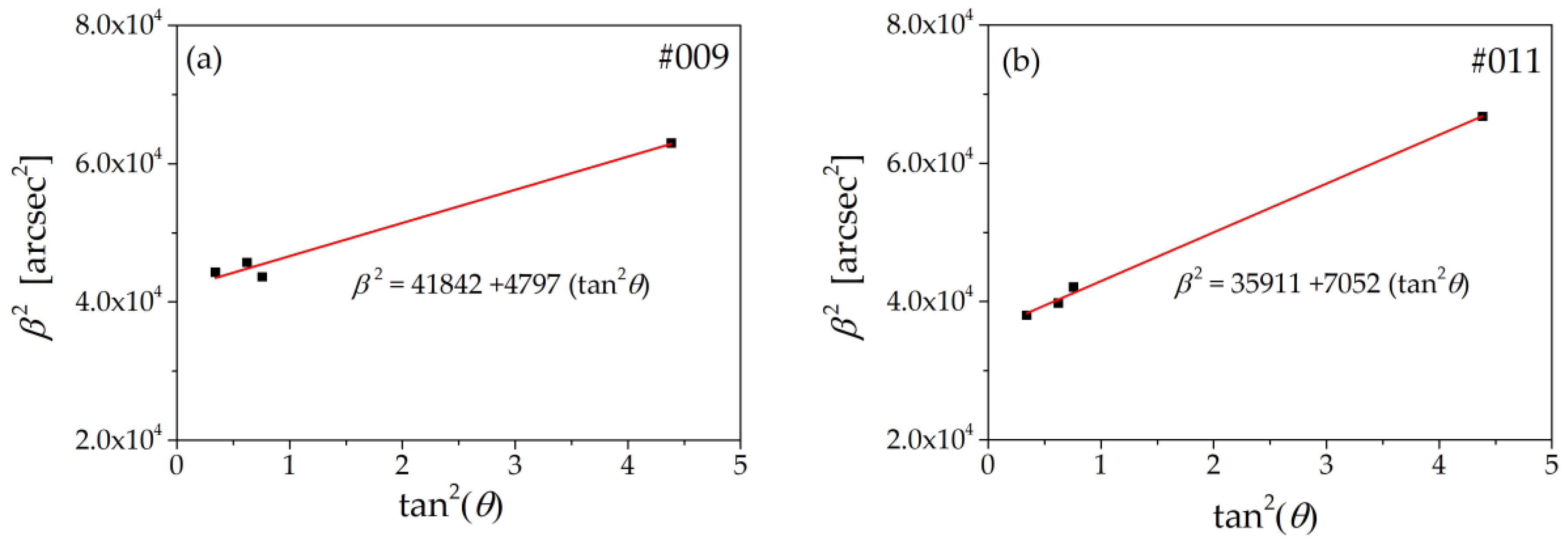
3.1. The Approach Based on HRXRD Measurements

In this approach, the dislocation densities were obtained by choosing (004), (-2-24), (115), and (117) reflections for calculations. The rocking curves and 2θ/ω scans were measured to determine the values of β and θ for each reflection. Due to the presence of 60° dislocations in the characterized structures, a factor of 0.160 instead of 0.090 was used in Equation (3), which is proper for this type of defect [12]. In our case, the Burgers vector is b = a L 2 2 . In Figure 1, a linear dependence of β2 on tan2θ for the metamorphic (#009) and IMF (#011) GaSb materials is shown.
As can be seen, the experimental data obtained for both samples fall on a straight line with the coefficients Kα = 41,842 arcsec2 = 9.825 × 10⁻⁷ rad2 and Kɛ = 4797 arcsec2 = 1.126 × 10⁻⁷ rad2 for #009 metamorphic GaSb layer and Kα = 35,911 arcsec2 = 8.432 × 10⁻⁷ rad2 and Kɛ = 7052 arcsec2 = 1.656 × 10⁻⁷ rad2 for #011 IMF-GaSb. Based on these coefficients, the dislocation densities for sample #009 is 4.85 × 108 cm−2 and 2.65 × 108 cm−2 as determined from angular and strain broadening, respectively. These values differ almost by a factor of 1.83. However, according to Ayers [13], such a difference can still be considered a very good agreement between the two independent calculations of the dislocation density. For other structures, the differences between the results of these two calculations were smaller, e.g., for sample #011, values of 4.16 × 108 cm−2 and 4.04 × 108 cm−2 were obtained. The same procedure was applied for all discussed structures, and the results are listed in Table 3.

3.2. The Approach Based on the Revealing of Etch Pits

The results obtained using etchant I were inconclusive. A nonuniform surface with uncharacterized morphology was observed. No shapes which could be identified as pits originating from dislocations appeared on the etched surface.
Etchant II caused the epilayer to be completely removed at the edges of the sample after 5 s. Additionally, there was a strong reaction on the surface during etching and constant stirring was necessary to remove gaseous products. This solution produced an over-etched surface with difficult to distinguish forms.
Etchant III also induced strong gaseous reactions on the surface of samples. Rectangular and triangular (marked using ellipses) pits were visible on SEM images (Figure 2a) after etching at 70 °C. Rectangular shapes with a density of about 5.3 × 107 cm−2 are similar to the stacking faults presented in Reference [25], while the triangular ones with a density of 2.4 × 106 cm−2 may be identified as dislocations. Decreasing the temperature to RT provided a surface image similar to the one obtained at 70 °C. Solution (III) gave reproducible etching behaviour, but it was better for evaluation of stacking-fault density rather than dislocation density.
The fourth solution (etchant IV) based on H2O2–H2SO4 did not reveal any dislocation pits and produced difficult to discern features. After one minute of etching, the solution caused formation of a bronze-coloured film on the GaSb surface, and after three minutes, total degradation of the layer occurred. It should be noted that none of the considered H2O2-based etchants proved to be satisfactory in revealing dislocation pits. For two solutions, the etching rate was too high, and the processes were either difficult to control or had to be stopped after several seconds. The etchants were also too aggressive for thin layers, and even if they revealed some pits, they did not originate from dislocations.
The last etchant (V) was optimized for a pure GaSb material only. It was useless for complex alloys (e.g., AlGaAsSb) or other binaries (AlSb, GaAs, and InAs). It allowed for revealing large etch pits associated with dislocations and visible under an optical microscope. These were also examined using SEM. As can be seen in Figure 2b, there are two types of pits originating from 60° misfit dislocations of alternating orientations. The estimated dislocation density was about 2.1 × 107 cm−2. It is noteworthy that etchant V, even though more difficult to prepare, after adjusting the etching time and temperature, gave an excellent reproducibility with well-defined triangular pits. In this case, only the trial for sample #007 failed.

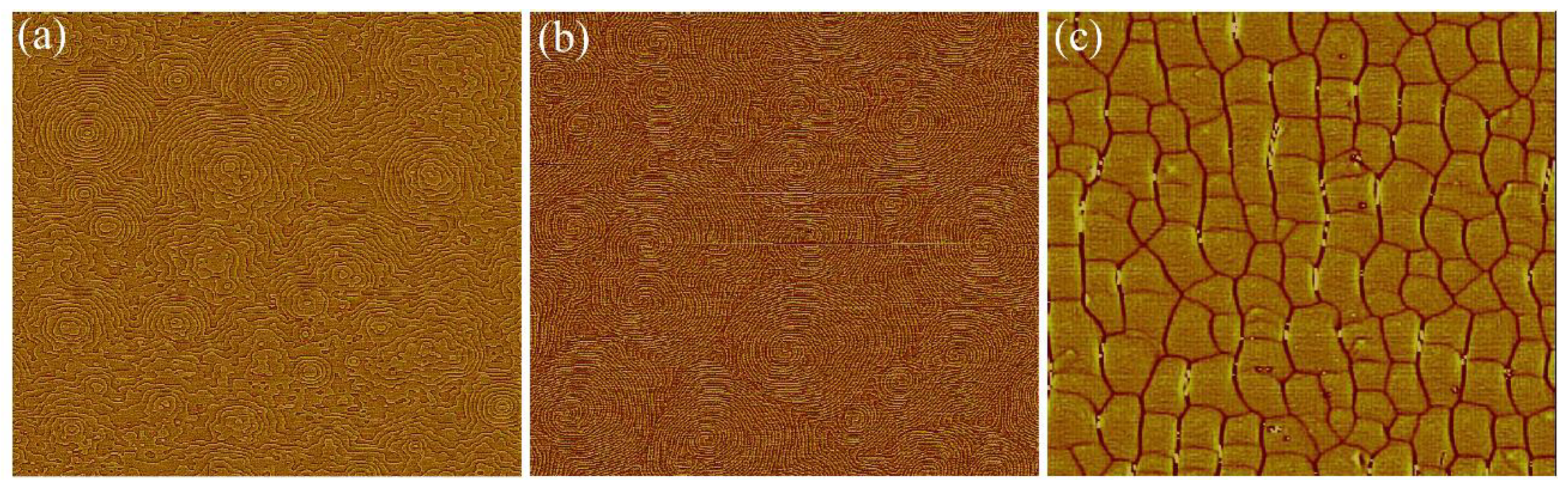
3.3. The Approach Based on Atomic Force Microscope (AFM) Observations

The AFM images are useful for determination of the growth mode. In Figure 3 (top view) and 4 (differential one), the differences between modes listed in Table 3 are visualized. In the case of spiral growth mode, there are characteristic tapers on the sample surfaces (Figure 4a,b). The image of the homoepitaxial surface revealed tapers with various base diameters and the terrace structure on the walls (Figure 4a). The taper density is 6.5 × 106 cm−2. The terrace structure forms concentric circles. Based on this, the dislocations with a screw component of the Burgers vector (screw or 60° dislocations) are not responsible for the occurrence of the tapers [19]. Thus, the dislocation density of the homoepitaxial material cannot be evaluated based on the AFM images. In the case of IMF-GaSb/GaAs, the tapers visible in Figure 4b consist of the 1 ML high terraces centred on top of the mounds and spreading outwards in a spiral manner. They intersect with similar terraces from the neighbouring mounds. It can be seen that, on average, two spirals originate from the centre of the tapers. Spiral growth occurs in the presence of mixed type threading dislocations with the screw component of the Burgers vector [4]. Assuming that, on average, one mound corresponds to two dislocations, the threading dislocation density can be easily estimated as 1.6 × 107 cm−2 for the analysed sample.
The differential scans presented in Figure 4 were used for showing more clearly the disparities between circle-shaped terraces forming cone-like tapers and cone-like tapers consisting of spiralling terraces.

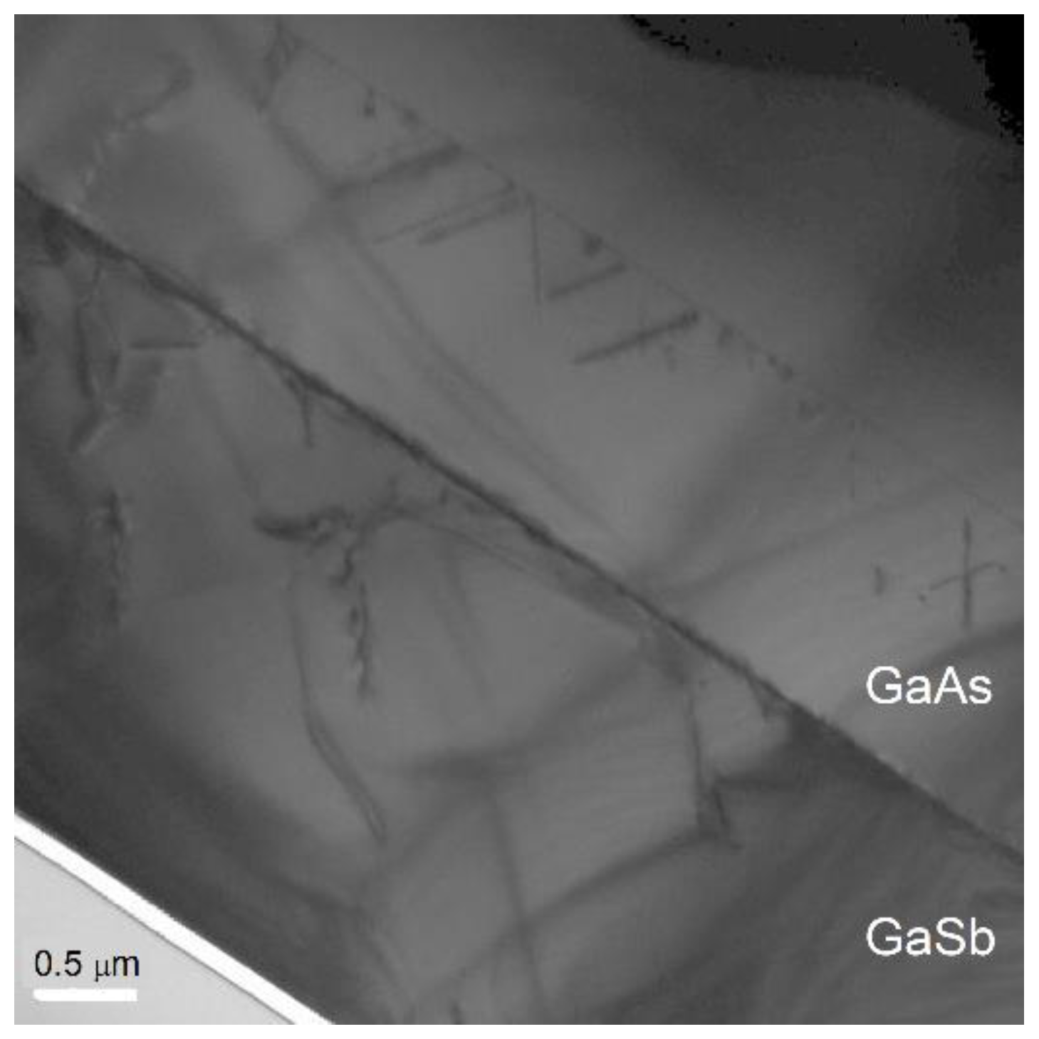
3.4. The Approach Based on High Resolution Transmission Electron Microscope (HRTEM) Observations

In general, threading dislocation density should be estimated based on planar images of a large area. Nevertheless, under the assumption that threading dislocations are uniformly distributed over the entire volume of GaSb material, the density can be also determined based on the TEM cross-sectional images. In Figure 5, the length of the GaSb/GaAs interface is about 4.0 μm. The number of dislocations in the field of view is about 30, which results in a TDD of 5.6 × 109 cm−2. It is an order of magnitude higher than the value determined using HRXRD (on average, 3.0 × 108 cm−2) and two orders of magnitude higher than the one obtained from counting etch pits or counting tapers on AFM images (about 4.0 × 107 cm−2). It is noteworthy that the regions of the material without any dislocations or with reduced dislocation density (by one order of magnitude) were also revealed by TEM analysis for sample #012. This indicates that the determination of TDD using HRTEM images may lead to either significant underestimation or overestimation of the results.

3.5. Discussion of Experimental Results

Some general conclusions can be drawn from the experimental data listed in Table 3. TDD calculations based on both angular and strain broadening of the rocking curve and using Kα and Kɛ coefficients determined from the experiment yielded similar results for all analysed structures with the dislocation density above 108 cm−2 (high dislocation density). In most cases (for 11 of 14 analysed samples), a bit higher DD was obtained using angular broadening of RC compared to the strain broadening approach. For samples with low DD (the substrates and the homoepitaxial structures), the differences between results obtained using these two approaches are one order of magnitude larger. It proves that the method based on HRXRD measurements is only valid for structures with high TDD. The compliance threshold is 108 cm−2. When the density of dislocations decreases below this value, the results obtained from HRXRD are no more valid for this system.
The highest obtained values of threading dislocation densities (mostly n × 108 cm−2) were determined using HRXRD measurements. It can be explained due to broadening of the rocking curve being influenced by all types of dislocations in a material volume including those at the interface region, whereas both the EPD and AFM techniques consider only the dislocations reaching the sample surface. The angular broadening approach in HRXRD measurements allowed for obtaining the results which were more consistent with data obtained using the other two techniques. Based on the comparison between AFM and EPD techniques (only for samples with the spiral growth mode: #011 ÷ #015 and #017 ÷ #020), the former gives higher values of DD (mostly n × 107 cm−2). Again, the AFM technique allows one to observe all dislocations with the screw component of Burgers vectors (screw and 60° dislocations); however, the etch pits originating only from 60° dislocations were taken into account (mostly n × 106 cm−2). The method based on counting of etch pits is a useful and practical tool due to its simplicity, reliability, and repeatability of the results.
More detailed remarks related to quantitative comparison inside this material system are listed below. It is noteworthy that EPD obtained for the GaSb substrate is about twice higher than the value given in the product specification (≤2 × 103 cm−2) provided by the supplier. Homoepitaxial structures differed in TDD (EPD results) and surface morphology (AFM results). Furthermore, thin sample #003 grown in 2D-T mode (1.0 μm-thick, 1 ML terraces on the surface) has four times lower DD, approximately 8 × 103 cm−2, than sample #005 grown in 3D mode (the tapers on the surface) and only twice higher than #001 GaSb substrate. Dislocation density for thick sample #004 (8.0 μm) was two orders of magnitude higher, approximately 2 × 106 cm−2, than for thin sample #005 with the tapers on the surface (DD approximately 3 × 104 cm−2) due to gradual degradation of the material quality after exceeding the thickness of 4.0 μm. Therefore, the EPD at first decreases with increasing layer thickness and then increases, which is in line with expectations. This dependence is not observed in the results obtained by HRXRD (DA, DS) so this method is not suitable for homoepitaxial material optimization. Investigation of the metamorphic structures M-GaSb/GaAs resulted in similar values of DD in thin (1.5 μm) and thick (8.0 μm) M-GaSb layers, assuming that dislocation densities determined using the EPD and AFM techniques for thin #015 M-GaSb were comparable. The lowest DD was obtained for the 4.0-μm M-GaSb layer (DA approximately 4 × 108 cm−2 and DEP approximately 4 × 105 cm−2). Both results point to degradation of crystal quality in GaSb layers thicker than 4.0 μm. For analysed samples, HRXRD results were similar regardless of their thickness due to the comparable DD near the GaSb/GaAs interfaces. As one can see, the results obtained by HRXRD (DA) and EPD (DEP) are consistent with each other and comply with assumptions. It indicates that both methods are useful for metamorphic material optimization.
Analysis of the crystal quality of IMF-GaSb/GaAs structures led to the following remarks. The thickest samples have the lowest DD regardless of the method of their evaluation. The medium thickness ones got intermediate values of DD, which was confirmed using all described techniques except for EPD. DA, DEP, and DAFM showed consistently the inverse relationship between DD and V/III for samples with 1.0 μm thickness, which is consistent with expectations. The results obtained for GaSb/IMF-LT-AlSb/GaAs structures showed a rise of DD with increasing LT-AlSb thickness using all three methods. It indicates that all methods are suitable for IMF-based material optimization.
The results obtained for AlSb and quaternary alloy deposited on a GaSb substrate were contradictory. Dislocation density determined from HRXRD measurements was higher for AlSb, while AFM observation revealed a higher number of tapers on the Al0.5GaAs0.05Sb surface. Meanwhile, very close values of DA and DAFM were obtained for the superlattice. The EPD is not suitable for determination of DD of complex heterostructures.
It is difficult to compare the obtained results with the findings of other researchers. The comparison must be taken between similar samples grown with the same method and investigated using the same technique. In addition, the layer thickness significantly influences DD. As such, despite the wealth of literature, it was only possible to make a comparison for HRXRD data. Similar HRXRD measurements were carried out and reported in Reference [11]. The dislocation density of about 108 cm−2 determined for a 2-μm-thick IMF-GaSb layer is close to the result obtained for our sample #011.

4. Conclusions

In this work, the threading dislocation density was studied in three groups of materials: the lattice-matched GaSb/GaSb, the lattice-mismatched GaSb/GaAs, and the complex GaSb-based heterostructures. Three approaches based on HRXRD measurements, the counting of etch pits, and tapers on SEM and AFM images were used. HRTEM was used only for selected samples due to the area limitations and time-consuming sample preparation and measurement.
The HRXRD approach utilizing the angular broadening of rocking curves gave dependencies of DD closer to the data obtained using the other two techniques than the one using the strain broadening of RC. The broadening of the rocking curve is influenced by all types of dislocations, which results in the highest values of DD among considered approaches. The AFM technique gave (only for samples with the spiral growth mode) higher values of DD in comparison with EPD. The AFM allows one for observation of the tapers originating from all dislocations with the screw component of Burgers vector (screw and 60° dislocations), while the etch pits originate only from the 60° dislocations. For example, the values of DD of 6.5 × 108 cm−2, 2.2 × 106 cm−2, and 4.1 × 107 cm−2 were obtained for sample #017 using the HRXRD (DA), EPD (DEP), and AFM (DAFM) techniques, respectively. Thus, the information on TDD should be provided together with information about the measurement method. Nevertheless, the absolute value of TDD is not as essential as the credibility of the method used for optimizing material growth. The general conclusions referring to appropriateness of using the considered method for determining the dislocation density in GaSb-based materials are as follows: HRXRD and AFM approaches are not suitable for homoepitaxial material optimization. In the first case, the main reason is that the dislocation density at the level below the resolution of the HRXRD method does not affect RC lineshape broadening. On the other hand, the lack of spiral growth in homoepitaxial materials prevents the use of AFM observations. Correct results were obtained using the EPD technique. In the case of heteroepitaxial layers, two methods, i.e., HRXRD based on the rocking curve broadening and EPD, are useful for metamorphic material optimization, and all tested techniques are suitable for IMF-based material optimization. From the last investigated group of complex heterostructures, unambiguous results were only obtained for the superlattice. The latter may be examined using the HRXRD (DA) and AFM methods. The EPD is not suitable for this purpose as no etch pits were revealed on their surface.

Author Contributions

Conceptualization, A.J.; methodology, A.J.; validation, A.J., K.C. and I.S.; formal analysis, A.J.; investigation, A.J., D.S., I.S., J.R., A.W. and P.K.; resources, A.J.; data curation, K.C.; writing—original draft preparation, A.J., D.S. and I.S.; writing—review and editing, A.J., K.C. and I.S.; visualization, A.J., K.C. and I.S.; supervision, A.J.; project administration, A.J.; funding acquisition, A.J. All authors have read and agreed to the published version of the manuscript.

Funding

This research was partially funded by the National Science Centre (NCN), project No. 2013/11/B/ST7/04341, and by the National Centre for Research and Development (NCBR), project No. TECHMATSTRATEG1/347751/5/NCBR/2017 and project No. POIR.04.01.04-00-0123/17-00.

Acknowledgments

The authors would like to thank K. Regiński for his support and assistance with these projects.

Conflicts of Interest

The authors declare no conflict of interest.

References

  1. Johnson, S.M. Effect of dislocations on the electrical and optical properties of long-wavelength infrared HgCdTe photovoltaic detectors. J. Vac. Sci. Technol. B Microelectron. Nanometer Struct. 1992, 10, 1499. [Google Scholar] [CrossRef]
  2. Dang, S.; Li, C.; Lu, M.; Guo, H.; He, Z. Threading dislocation density effect on the electrical and optical properties of InGaN light-emitting diodes. Optik 2018, 155, 26–30. [Google Scholar] [CrossRef]
  3. Dai, Q.; Schubert, E.F.; Kim, M.H.; Kim, J.K.; Koleske, D.D.; Crawford, M.H.; Lee, S.R.; Fischer, A.J.; Thaler, G.T.; Banas, M.A. Internal quantum efficiency and nonradiative recombination coefficient of GaInN/GaN multiple quantum wells with different dislocation densities. Appl. Phys. Lett. 2009, 94, 111109. [Google Scholar] [CrossRef] [Green Version]
  4. Wang, Y.-L.; Ruterana, P.; Kret, S.; El Kazzi, S.; Desplanque, L.; Wallart, X. The source of the threading dislocation in GaSb/GaAs hetero-structures and their propagation mechanism. Appl. Phys. Lett. 2013, 102, 052102. [Google Scholar] [CrossRef]
  5. Huang, S.; Khoshakhlagh, A.; Jallipalli, A.; Dawson, L.; Balakrishnan, G.; Huffaker, D. Strain relief by periodic misfit arrays for low defect density GaSb on GaAs. Appl. Phys. Lett. 2006, 88, 131911. [Google Scholar] [CrossRef] [Green Version]
  6. Jasik, A.; Sankowska, I.; Wawro, A.; Ratajczak, J.; Jakiela, R.; Pierścińska, D.; Smoczyński, D.; Czuba, K.; Regiński, K. Comprehensive investigation of the interfacial misfit array formation in GaSb/GaAs material system. Appl. Phys. A 2018, 124, 512. [Google Scholar] [CrossRef] [Green Version]
  7. Jasik, A.; Sankowska, I.; Ratajczak, J.; Wawro, A.; Smoczyński, D.; Czuba, K.; Wzorek, M. Atomically smooth interfaces of type-II InAs/GaSb superlattice on metamorphic GaSb buffer grown in 2D mode on GaAs substrate using MBE. Curr. Appl. Phys. 2019, 19, 120–127. [Google Scholar] [CrossRef]
  8. Huang, S.; Balakrishnan, G.; Huffaker, D.L. Interfacial misfit array formation for GaSb growth on GaAs. J. Appl. Phys. 2009, 105, 103104. [Google Scholar] [CrossRef]
  9. Jallipalli, A.; Balakrishnan, G.; Huang, S.H.; Rotter, T.J.; Nunna, K.; Liang, B.L.; Dawson, L.R.; Huffaker, D.L. Structural Analysis of Highly Relaxed GaSb Grown on GaAs Substrates with Periodic Interfacial Array of 90° Misfit Dislocations. Nanoscale Res. Lett. 2009, 4, 1458–1462. [Google Scholar] [CrossRef] [Green Version]
  10. Tan, K.; Jia, B.W.; Loke, W.; Wicaksono, S.; Yoon, S. Formation of interfacial misfit dislocation in GaSb/GaAs heteroepitaxy via anion exchange process. J. Cryst. Growth 2015, 427, 80–86. [Google Scholar] [CrossRef]
  11. Benyahia, D.; Kubiszyn, Ł.; Michalczewski, K.; Kębłowski, A.; Martyniuk, P.; Piotrowski, J.; Rogalski, A. Interfacial Misfit Array Technique for GaSb Growth on GaAs (001) Substrate by Molecular Beam Epitaxy. J. Electron. Mater. 2017, 47, 299–304. [Google Scholar] [CrossRef] [Green Version]
  12. Stirland, D.J. Quantitative defect etching of GaAs on Si: Is it possible? Appl. Phys. Lett. 1988, 53, 2432–2434. [Google Scholar] [CrossRef]
  13. Ayers, J. The measurement of threading dislocation densities in semiconductor crystals by X-ray diffraction. J. Cryst. Growth 1994, 135, 71–77. [Google Scholar] [CrossRef]
  14. Papis-Polakowska, E. Surface treatments of GaSb and related materials for the processing of mid-infrared semiconductor devices. Electron Technol. 2005, 37, 1–34. [Google Scholar]
  15. Brown, G.T.; Cockayne, B.; MacEwan, W.R.; Steward, V.W. A defect etchant for single crystal GaSb. J. Mater. Sci. Lett. 1982, 1, 253–256. [Google Scholar] [CrossRef]
  16. Cockayne, B.; Steward, V.; Brown, G.; MacEwan, W.; Young, M.; Courtney, S. The Czochralski growth of gallium antimonide single crystals under reducing conditions. J. Cryst. Growth 1982, 58, 267–272. [Google Scholar] [CrossRef]
  17. Reijnen, L.; Brunton, R.; Grant, I. GaSb single-crystal growth by vertical gradient freeze. J. Cryst. Growth 2005, 275, e595–e600. [Google Scholar] [CrossRef]
  18. Costa, E.; DeDavid, B.; Müller, A. Investigations of structural defects by etching of GaSb grown by the liquid-encapsulated Czochralski technique. Mater. Sci. Eng. B 1997, 44, 208–212. [Google Scholar] [CrossRef]
  19. Brar, B.; Leonard, D. Spiral growth of GaSb on (001) GaAs using molecular beam epitaxy. Appl. Phys. Lett. 1995, 66, 463–465. [Google Scholar] [CrossRef]
  20. Jasik, A.; Kubacka-Traczyk, J.; RegińskiK; Sankowska, I.; Jakieła, R.; Wawro, A.; Kaniewski, J. Method of determination of AlGaAsSb layer composition in molecular beam epitaxy processes with regard to unintentional As incorporation. J. Appl. Phys. 2011, 110, 073509. [Google Scholar] [CrossRef]
  21. Grabmaier, J.G.; Watson, C.B. Dislocation Etch Pits in Single Crystal GaAs. Phys. Status Solidi (b) 1969, 32, K13–K15. [Google Scholar] [CrossRef]
  22. Weiss, E.; Klin, O.; Grossmann, S.; Snapi, N.; Lukomsky, I.; Aronov, D.; Yassen, M.; Berkowicz, E.; Glozman, A.; Klipstein, P.C.; et al. InAsSb-based XBnn bariodes grown by molecular beam epitaxy on GaAs. J. Cryst. Growth 2012, 339, 31–35. [Google Scholar] [CrossRef]
  23. Gatos, H.C.; LaVine, M.C. Characteristics of the {111} Surfaces of the III–V Intermetallic Compounds. J. Electrochem. Soc. 1960, 107, 427. [Google Scholar] [CrossRef]
  24. Mirowska, A.; Orłowski, W.; Bańkowska, A.; Hruban, A. Growth of gallium antimonide single crystals in and directions by Czochralski method. Mater. Elektron. 2009, 37, 3. [Google Scholar]
  25. Kodama, M. Defect evaluation and electrical characteristics of GaSb and In0.17Ga0.83Sb films grown by molecular beam epitaxy. Phys. Status Solidi (a) 1994, 141, 145–154. [Google Scholar] [CrossRef]
Figure 1. Linear dependence of β2 vs tan2(θ) for metamorphic #009 (a) and interfacial misfit array (IMF) #011 (b) GaSb materials.
Crystals 10 01074 g001
Figure 2. SEM images of #009 sample: the rectangular and triangular (marked) etch pits originating from the stacking faults and the dislocations, respectively (a), and two types of triangular etch pits originating from 60° misfit dislocations of alternating orientations (b).
Crystals 10 01074 g002
Figure 3. AFM top view (10 μm × 10 μm) of a 2D surface for #001 GaSb substrate (a), 2D-T mode for #003 homoepitaxial (b), and 3D mode for #009 metamorphic (c) GaSb samples.
Crystals 10 01074 g003
Figure 4. AFM differential images (20 μm × 20 μm) of GaSb surfaces grown in 3D spiral mode for #005 homoepitaxial GaSb (a), #011 IMF-GaSb (b), and #016 IMF-GaSb (c) samples.
Crystals 10 01074 g004
Figure 5. TEM cross section of #012 GaSb/GaAs heterostructure: the thicker region (lower part of the image) corresponds to the GaSb material. TDD is 5.6 × 109 cm−2.
Crystals 10 01074 g005
Table 1. Structures used for evaluating the threading dislocation density.
No.Thickness
(μm)
Material System
Substrates
#001450p-type GaSb (100) ± 0.1°, undoped, one side polished,
EPD ≤ 2 × 103 cm−2
#002450n-type GaAs (100) ± 0.5°, one side polished, EPD ≤ 5 × 102 cm−2
Group 1: homoepitaxial layers (GaSb/GaSb)
#0031.0thin and thick layers grown under optimized conditions
#0048.0
#0051.0thin layers grown under non-optimized conditions
#0061.0
Group 2: heteroepitaxial structures
heteroepitaxial metamorphic systems (M-GaSb/GaAs)
#0071.5layers with different thicknesses
#0084.0
#0098.0
heteroepitaxial structures deposited on GaAs substrates using interfacial misfit array (IMF-GaSb/GaAs) with different GaSb layer thickness
#0104.0thick
#0112.0medium
#0122.5medium
#0131.0thin (V/III = 2.3)
#0141.0thin (V/III = 2.9)
#0151.0thin (V/III = 3.2)
#0165.0thick
heteroepitaxial structures deposited on GaAs substrates using IMF and low-temperature (LT) AlSb interlayer with different thicknesses (GaSb/LT-AlSb/GaAs)
#0171.01.0 nm
#0181.02.0 nm
#0191.030.0 nm
Group 3: complex heterostructures
#0200.5IMF-AlSb/GaAs heterostructure
#0211.0Al0.5Ga0.5As0.05Sb0.95 layer deposited on GaSb substrate
#02230 × (57.9 × 10-4)InAs/GaSb superlattice deposited on GaSb substrate (thicknesses of InAs and GaSb layers in SL were 8 and 9 monolayers (ML), respectively)
Table 2. Etchants used for revealing etch pits in (100) GaSb epilayer. RT (room temperature).
NoEtchantsReferencesEtching Conditions
RatioTemperatureTime (s)Rate (nm/s)
I20% KOH[5]25 g diluted in 100 mL of H2ORT and 80 °C1800-
IIH2O2-HCl[15]2:1RT15180–150
IIIH2O2-HCl-H2O[17,22]2:4:1RT and 70 °C1200/152/135
IVH2O2-H2SO4[18]1:510 °C18015
VFeCl3 (0.13 M)-HCl (13 M)[24]-RT and 40 °C6015
Table 3. The threading dislocation density for different structures using three methods: high-resolution x-ray diffraction (HRXRD) (DA and DS), etch pit density (EPD) (DEP), and atomic force microscopy (AFM) (DAFM).
NoThreading Dislocation Density (cm−2)
DADSDEPDAFM
Substrates
#0012.5 × 1068.1 × 1073.7 × 1032D
#0021.8 × 1071.5 × 108-2D
Group 1: homoepitaxial layers (GaSb/GaSb)
#0038.1 × 1061.1 × 1087.6 × 1032D-T
#0048.5 × 1061.0 × 1082.4 × 1063D
#0059.3 × 1068.9 × 1072.2 × 1046.5 × 106 (t/c)
#0069.5 × 1069.3 × 1073.6 × 1041.2 × 108 (t/c)
Group 2: heteroepitaxial structures
heteroepitaxial metamorphic systems (M-GaSb/GaAs)
#0074.9 × 1083.4 × 108failed3.6 × 107
#0084.1 × 1083.3 × 1084.0 × 1052D-T
#0094.8 × 1082.6 × 1082.1 × 1073D
heteroepitaxial structures deposited on GaAs substrates using interfacial misfit array (IMF-GaSb/GaAs) with different GaSb layer thicknesses
#0101.9 × 1082.0 × 1089.3 × 1062D-T
#0114.2 × 1084.0 × 1081.4 × 1071.6 × 107
#0122.6 × 1083.4 × 1084.3 × 1074.6 × 107
#0137.3 × 1085.9 × 1088.5 × 1067.8 × 106
#0141.0 × 1095.6 × 1084.5 × 1077.4 × 107
#0151.1 × 1094.8 × 1087.0 × 1071.2 × 108
#0161.5 × 1083.4 × 1089.7 × 1061.6 × 108 (c)
heteroepitaxial structures deposited on GaAs substrates using IMF and low-temperature (LT) AlSb interlayer with different thicknesses (GaSb/LT-AlSb/GaAs)
#0176.5 × 1085.6 × 1082.2 × 1064.1 × 107
#0187.2 × 1085.7 × 1082.4 × 1065.1 × 107
#0199.2 × 1084.7 × 1083.0 × 1067.1 × 107
Group 3: complex heterostructures
#0202.8 × 1092.7 × 109-4.0 × 10⁷
#0215.6 × 1088.0 × 108-7.6 × 10⁷
#0223.2 × 1086.8 × 108-1.0 × 10⁸
Publisher’s Note: MDPI stays neutral with regard to jurisdictional claims in published maps and institutional affiliations.

