Article

The Influence of Deposition Time on the Structural, Morphological, Optical and Electrical Properties of ZnO-rGO Nanocomposite Thin Films Grown in a Single Step by USP

by
R. Ramírez-Amador
1,7,*,
J. Alvarado
1,*,
G. Flores-Carrasco
2,
L. Morales-de la Garza
3,
S. Alcántara-Iniesta
1,
A. Luna-Flores
4,
Y. P. Bernal
1,
Miguel Ángel Méndez Rojas
5,
J. J. Gervacio-Arciniega
6,
H. P. Martínez Hernández
1,
J. F. Curioca-Vega
7 and
J. Balcón-Camacho
7
1
Center for Research in Semiconductor Devices (CIDS-ICUAP), Benemérita Universidad Autónoma de Puebla (BUAP), Av. San Claudio y 14 sur, Edif. 103C C.U., Col. San Manuel, 72570 Puebla, Mexico
2
Higher Technological Institute of Tepeaca, National Technological of Mexico, 75219 Tepeaca, Mexico
3
Center of Nanosciences and Nanotechnology (CNyN), National Autonomous University of Mexico (UNAM), Tijuana-Ensenada Highway km107, Playitas, 22860 Ensenada, Mexico
4
Faculty of Chemical Engineering, Benemérita Universidad Autónoma de Puebla (BUAP), Av. San Claudio y 14 sur, Col. San Manuel, 72570 Puebla, Mexico
5
Department of Chemical-Biological Sciences, University of the Americas Puebla, ExHda. Sta. Catarina Martir s/n, San Andrés Cholula, 72810 Puebla, Mexico
6
Conacyt-Faculty of Mathematical Physics Sciences (FCFM), Benemérita Autonomous University of Puebla (BUAP), Av San Claudio, Edif. FM6, C. U., Jardines de San Manuel, 72572 Puebla, Mexico
7
Mechatronics Career, Technological University of Huejotzingo (UTH), Real San Mateo 36B, Second Secc, Santa Ana Xalmimilulco, 74169 Puebla, Mexico
*
Authors to whom correspondence should be addressed.
Crystals 2020, 10(2), 73; https://doi.org/10.3390/cryst10020073
Submission received: 26 November 2019 / Revised: 20 January 2020 / Accepted: 20 January 2020 / Published: 29 January 2020

Abstract

:
Thin films of nanocomposite of zinc oxide–reduced graphene oxide (ZnO-rGO) deposited on soda-lime glass substrates were prepared using ultrasonic spray pyrolysis (USP) at 460 °C. The preparation process does not use harsh acids and is environmentally friendly. The deposition period of 2, 3.5 and 5 min resulted in compact, uniform samples with thicknesses of 148, 250 and 365 nm, respectively. After performing structural, morphological, optical and electrical characterization of the prepared nanocomposite, an influence of the deposition time on the physical properties of the obtained films was determined. TEM analyses indicate that the ZnO-rGO nanocomposite presents ZnO nanoparticles anchored on graphene sheets, while XRD, X-ray Photoelectron Spectroscopy (XPS) and Raman results show the presence of a ZnO phase in the ZnO-rGO films. HR-SEM studies showed changes of the ZnO-rGO thin films morphology due to the incorporation of graphene into the ZnO films. Here, the particles of ZnO are similar to small grains of rice and graphene films have the appearance of a little “rose”. As the thickness of the film increases with deposition time, it reduces the structure of resistance of the nanocomposite thin films to 135 Ω. In addition, the optical transmission of the thin films in the visible region resulted affected. Here, we report a simple methodology for the preparation of ZnO-rGO nanocomposite thin films.

1. Introduction

Graphene (G), a material with a unique structure formed by a single layer of carbon atoms arranged in a hexagonal honeycomb lattice, is fascinating due to its unique mechanical, thermal, optical and electrical properties [1,2]. In recent years, hybrid nanocomposites based on graphene presenting enhanced physical properties, have been developed and explored for applications as component in optoelectronic devices, energy storage, renewable energy and sensors [3]. One of the most studied functional hybrid nanocomposites is that formed by zinc oxide (ZnO) and graphene, due to its technologically potential applications [2]. ZnO has a wide bandgap energy (3.37 eV), large exciton binding energy (60 meV), and it can be synthesized in various morphologies, among others interesting physical and chemical characteristics [4,5].
This type of hybrid nanocomposite has attracted much interest mainly due to its highly active surfaces, excellent carrier mobilities and its effective charge-transfer process [6]. Due to these properties, it can be used as a component in ultraviolet photodetectors, transparent electrodes, biomedical sensors, white light-emitting diodes (LEDs), photovoltaic devices, photoluminescent material, gas sensors, photocatalysis, supercapacitors and optical switches [3,6,7,8,9,10,11,12,13,14].
Several methods are available for the preparation of graphene and its derivatives, being epitaxial growth and exfoliation two of the most commonly used [15]. The chemical reduction of exfoliated graphene oxide has been shown to be an effective and reliable, low cost and easily scalable method to produce graphene sheets. The use of this process for the preparation of hybrid nanocomposites, through the incorporation of various types of functional materials has been reported [16,17].
There are several methods that have been explored for binding reduced graphene oxide (rGO) flakes and ZnO nanoparticles. This is crucial for attaining an electronic interaction and inter-electron transfer at the interface of both materials [18]. For this purpose, hydrothermal [19], aerosol spraying [10], in situ preparation during refluxing [11], microwave irradiation assisted [18] and solvothermal [20] methods have been explored. Although, several routes have been used to prepare ZnO–G, ZnO-GO or ZnO-rGO nanocomposites. However, there are still some disadvantages when using graphene synthesized via the Hummers method. This method involves harsh acid treatments, followed by chemical reduction producing the rGO. As a result, it allows the formation of oxygen-containing functional groups on the graphene surface. The presence of these oxygenated groups results in significant compositional and structural defects that reduce its electrical properties [16,17] and also, it is harmful to humans, as well as, to the environment.
Although the ultrasonic spray pyrolysis (USP) allows the simultaneous oxidation and reduction of graphene in a single method, it has been scarcely reported. Furthermore, the use of inert atmospheres or other sophisticated techniques is not required for it [21,22]. In addition, USP competes with other commonly used techniques due its low cost and the good physical properties of the obtained product [23], aside that is a process well suited for large-scale production, which is desirable for industrial applications [24].
In this work, we present a simple method for the preparation of thin films of zinc oxide-reduced graphene oxide nanocomposite by USP, with no requirement of chemically oxidize graphene or the use of sodium hydroxide to attach the ZnO nanoparticles to the sheets of graphene. Only a solvent was used for the material exfoliation at room temperature (RT), whereas to obtain thin films, a low-temperature deposition by USP was used. As a result, this work demonstrates that when the thickness of the ZnO-rGO thin films increases, a modification in their structural, morphological, optical and electrical properties occurs, offering a potential use for different practical applications.

2. Experimental

2.1. Materials

Graphite flakes (GF, 99% carbon purity, Sigma-Aldrich) and zinc acetate dihydrate (Zn(CH3COO)2·2H2O, purity >98%, Sigma-Aldrich) were used as graphene and zinc oxide precursors, respectively. High-purity methanol (CH3OH, Merck) and deionized water (18.2 MΩ-cm) were used for the preparation of solutions. All chemicals were used as received without further purification.
Soda-lime glass (Corning, each of 1 × 1 cm2 area) was used to deposit the thin films. Cleaning of the substrates was carried out with a solution of hydrogen peroxide and sulfuric acid (1:3), then with hydrofluoric acid at 10%. Followed, by a cleaning process with deionized water in an ultrasonic cleaning bath and, finally, dried with a flow of dry air.

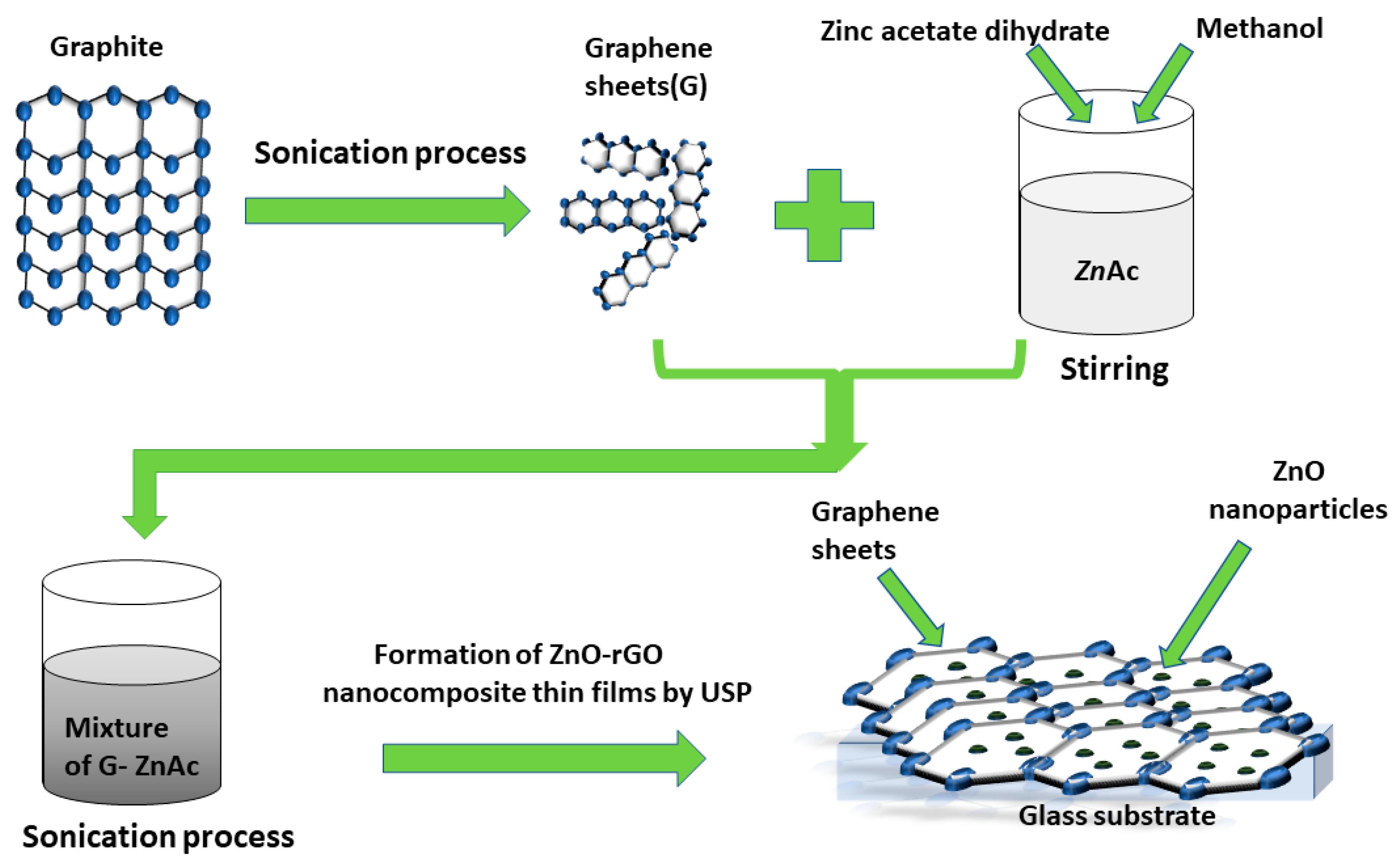
2.2. Synthesis of Graphene

Graphene was synthesized via the liquid phase exfoliation method. In a typical preparation, 50 mg graphite was dispersed in 100 mL of methanol and deionized water (2:3) solution. Then, it was sonicated at RT for 4 h to form a darkish black suspension. An ultrasonic probe working at 20 KHz with 50% amplitude (Q500 Sonicator 500 W, QSonica, Newtown, CT, USA) was used for the exfoliation of graphene in the aqueous solution. Next, the dispersions were centrifuged at 1000 rpm for 30 min to remove unexfoliated graphite flakes; the procedure was repeated several times. After that, the aqueous suspension was heated at 80 °C for 10 h, to evaporate the solvent.

2.3. Deposition Process of ZnO-rGO Nanocomposite Thin Films by USP

For the preparation of ZnO-rGO nanocomposite thin films, first, a precursor solution of Zn(CH3COO)2·2H2O (0.2 M) was prepared by dissolving the required amount of the zinc(II) precursor in methanol at room temperature. Then, the solution was vigorously stirred for 30 min at room temperature to yield a transparent solution. Second, the obtained solution was mixed with graphene, with a molar relation of graphene/Zn of 0.5 M. Then, the mixture was sonicated for the other 60 min to get a homogeneous solution. After that, it was possible to get GO with zinc oxide. The complete process is summarized in Scheme 1.
Furthermore, the mixture of zinc acetate (ZnAc) and GO was vaporized with an ultrasonic nebulizer (ultrasonic power of 100-watt, which had a resonance frequency of 1.2 MHz). Then, the generated mist was transported by the carrier gas (air), with a flow rate of 0.275 LPM (Omega Flow Controller Model FL1804, Daphne, AL, USA), through a nozzle to the preheated substrate at 460 °C. The nozzle consists of borosilicate glass, with 1.27 cm in diameter and 20 cm in length. The distance between the nozzle to the substrate was 2 cm, whereas the flow rate of the solution remained constant. Scheme 2 shows a schematic diagram of the USP system.
The spraying process involves various short cycles to avoid a decrease in the substrate temperature. When the mist (small droplets of the ZnAc and GO mixture) approach to the preheated substrate, the solvent rapidly evaporates, and a mixture decomposition occurs. The droplets were pyrolyzed, which allows the activation of chemical compounds producing solid thin films of ZnO-rGO under different experimental conditions. Table 1 shows a summary of these conditions. It is worth to note that, according to [25], it is possible to get rGO thin films when the GO thin films are heated in a reducing environment at 460 °C for 5 min.
The reaction for the formation of the material is described in Equation (1) [26,27]:
Zn ( CH 3 COO ) 2 Δ ZnO + C 3 H 6 O + C O 2 .

2.4. Characterization

The X-ray diffraction analysis was performed in a Bruker model D8 ADVANCE diffractometer with Cu Kα radiation (λ = 1.5418 Å), 40 kV-40 mA. Data was taken for the 2θ range of 10–80 degrees with a step of 0.01 degrees. The XRD data was analyzed with the JADE software (Materials Data, Inc., 1998, Livermore, CA, USA). The morphology and microstructure were characterized with a high-resolution scanning electron microscope (HRSEM) MAIA 3 (TESCAN, Czech Republic), which is equipped with a Bruker Quantax 200 energy dispersive spectroscopy (EDS) detector (Bruker, Berlin, Germany). Then, thin films were mounted on top of an aluminum base with a double conductive graphite tape and analyzed using a 15 keV electron beam. Transmission electron microscope (TEM) images were obtained on a JEOL J-2100F electron microscope JEOL, Japan) at an acceleration voltage of 200 kV. JEOL; the samples were prepared by depositing one drop of the nanocomposite in methanol on a carbon-coated copper grid and allowing the solvent to evaporate at room temperature. The surface topography of the thin films was obtained by a XE7 Park Systems Atomic Force Microscopy (AFM) (Park Systems Corp., Suwon, Korea) using a contact force of 1 nN. The study of chemical states of the samples was obtained using a Specs spectrometer (Germany). This has a hemispherical Phoibos-150-mcd-9 analyzer. As a Focus-500 (AlKα radiation, hλ = 1486.74 eV, 200 W radiation power) monochromator, with pressure is 1 × 10⁻⁹ Torr, with step energy of 0.1 eV. Raman scattering characterizations were obtained by a Horiba Scientific, Xplora Raman spectrometer (Horiba Scientific, Shanghai, China) with a 532 nm Nd-Yang excitation source. The transmittance of thin films was measured with a UV-visible spectrometer (Agilent, Model: Cary 5000, Santa Clara, CA, USA). The photoluminescence (PL) measurements were performed at room temperature using a solid-state violet laser (405 nm, 3.06 eV) with 60 mW. For the electrical characterization with UV response, a Keithley 4200 electric measurement system (Keithley, CA, USA) was used with a lamp (l = 325 nm) and a power consumption of 45 W at 8 cm from the sample. The thickness of thin films was measured using an "Alpha-step" surface profilometer (Alpha Step 200, Bufallo, NY, USA).

3. Results and Discussion
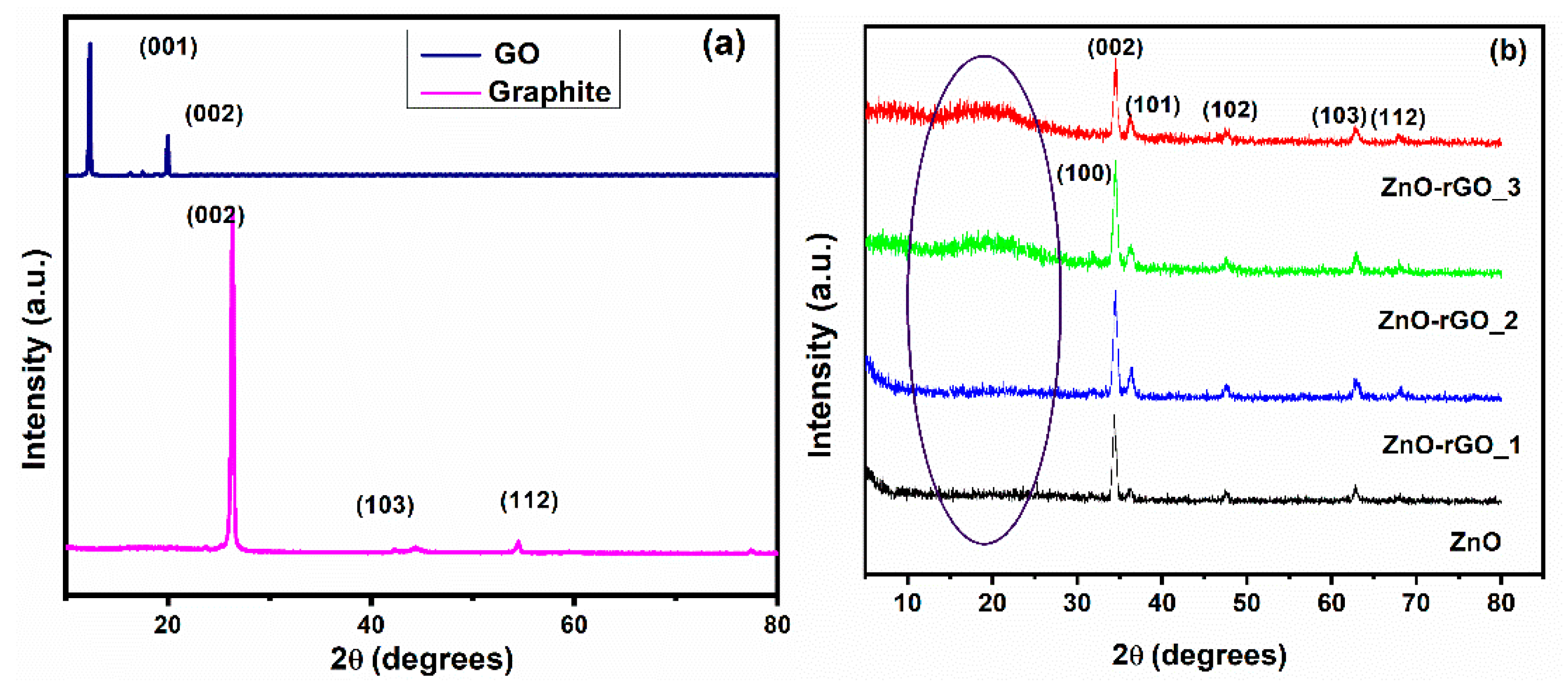
3.1. XRD Analysis

Figure 1a shows the XRD patterns of pure graphite and GO obtained in this work by ultra-sonication. XRD pattern of pure graphite shows a sharp peak at 2θ value of 26.50° and two other weak peaks at 2θ values of 44.38° and 54.46° (JCPDS 01-075-1621) [28]. GO presents two peaks at 2θ value of 12.2° and 20.10°. The first peak suggests the presence of corrugated locally parallel layers with lower crystallinity than that observed in graphite [29]. It has been reported that a sharp peak around 12.2° corresponds to an interlayer spacing of 0.78 nm, an indication that the graphite has been totally transformed into GO, with most oxygen atoms bound to the surface of GO [30]. The second peak at 20.10° may indicate that the GO sheets are not fully interconnected with oxygen atoms [31], which is in agreement with not using chemical agents for oxidizing graphene.
Figure 1b, presents the XRD patterns of ZnO and ZnO-rGO nanocomposite thin films. These diffractograms consists of six diffraction peaks at 32.6°, 34.3°, 36.8°, 47.5°, 62.8° and 67.9°, which belong to the (100), (002), (101), (102), (103) and (112) planes of the hexagonal wurtzite zinc oxide phase (JCPDS 36-1451), respectively [32]. The XRD pattern of thin films shows a preferential growth orientation along the (002) plane, indicating that the growth of the films is perpendicular to the substrate [33], with a 55.01%, 54.8%, 55.9% and 53.9% of preference for ZnO, ZnO-rGO_1, ZnO-rGO_2 and ZnO-rGO_3, respectively.
From the XRD pattern of the ZnO-rGO nanocomposite thin films (Figure 1b), it was expected to observe the peak corresponding to the typical GO (001) plane around 2θ = 12.2°. However, this peak was not detected, maybe due to the reduction of GO during the ultrasonic process or as a consequence of the interruption of the regular stack of GO sheets due to the intercalation of Zn2+ [34]. The disappearance of the diffraction peak at 12.2° implies that functional groups have been removed from the GO surface during the deposition of the film by UPS. However, this peak was not observed also for ZnO-rGO films with a thickness of 150 nm, and only a small, wide peak appeared around 2θ = 20° when the thickness of the films increased to 250 nm (Figure 1b). These changes in the diffraction patterns indicate the successful transformation from GO to rGO during the UPS deposition process. The disappearance of the peaks at 12.2° may be an indication of the reduction of GO to rGO when it is deposited as thin films, as a consequence of the deposition temperature and time. The operating conditions of the USP technique guarantee the presence of oxygen (from air) and a high temperature (460 °C) [25], to form GO in solution from the oxidation of the dispersed graphene and, then, reduce it to rGO when it is deposited on the film.
Table 1, compares some of the structural parameters for the ZnO and ZnO-rGO thin films according to their determined thicknesses and deposition time. The calculated average crystallite sizes (D) of ZnO-rGO nanocomposite thin films and residual error fit (R), along the preferentially oriented crystal plane were calculated to be around 17 nm. Both the ZnO and ZnO-rGO_1 samples showed smaller crystallites than the ZnO-rGO_2 and ZnO-rGO_3 samples. This may be due to the smaller thickness of ZnO, and ZnO-rGO_1 samples compared with the ZnO-rGO-2 and ZnO-rGO_3 films. As a result, the crystallite size in the films increases with the increment of the film’s thickness, which is in accordance with Flores-Carrasco et al. [35].

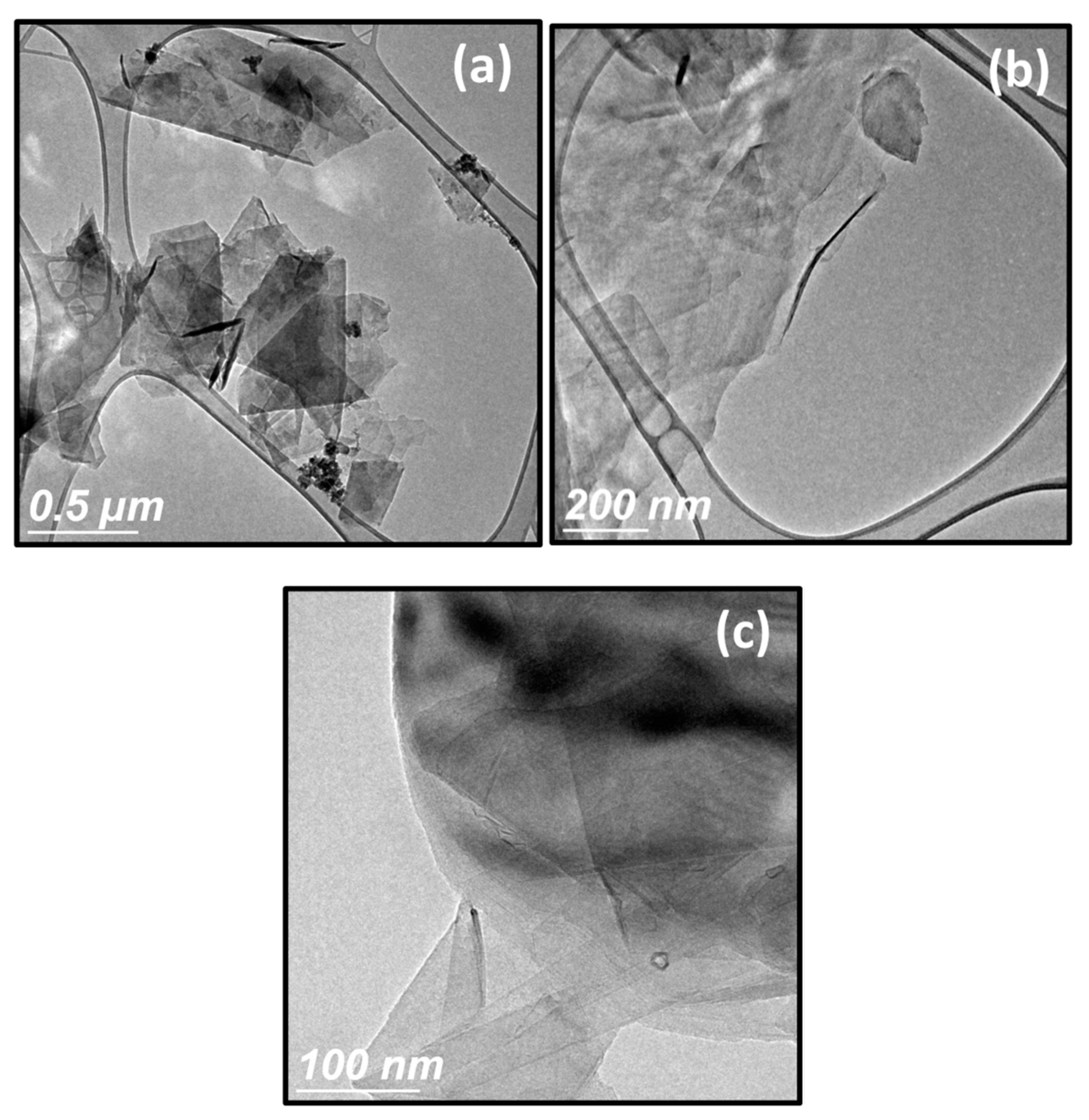
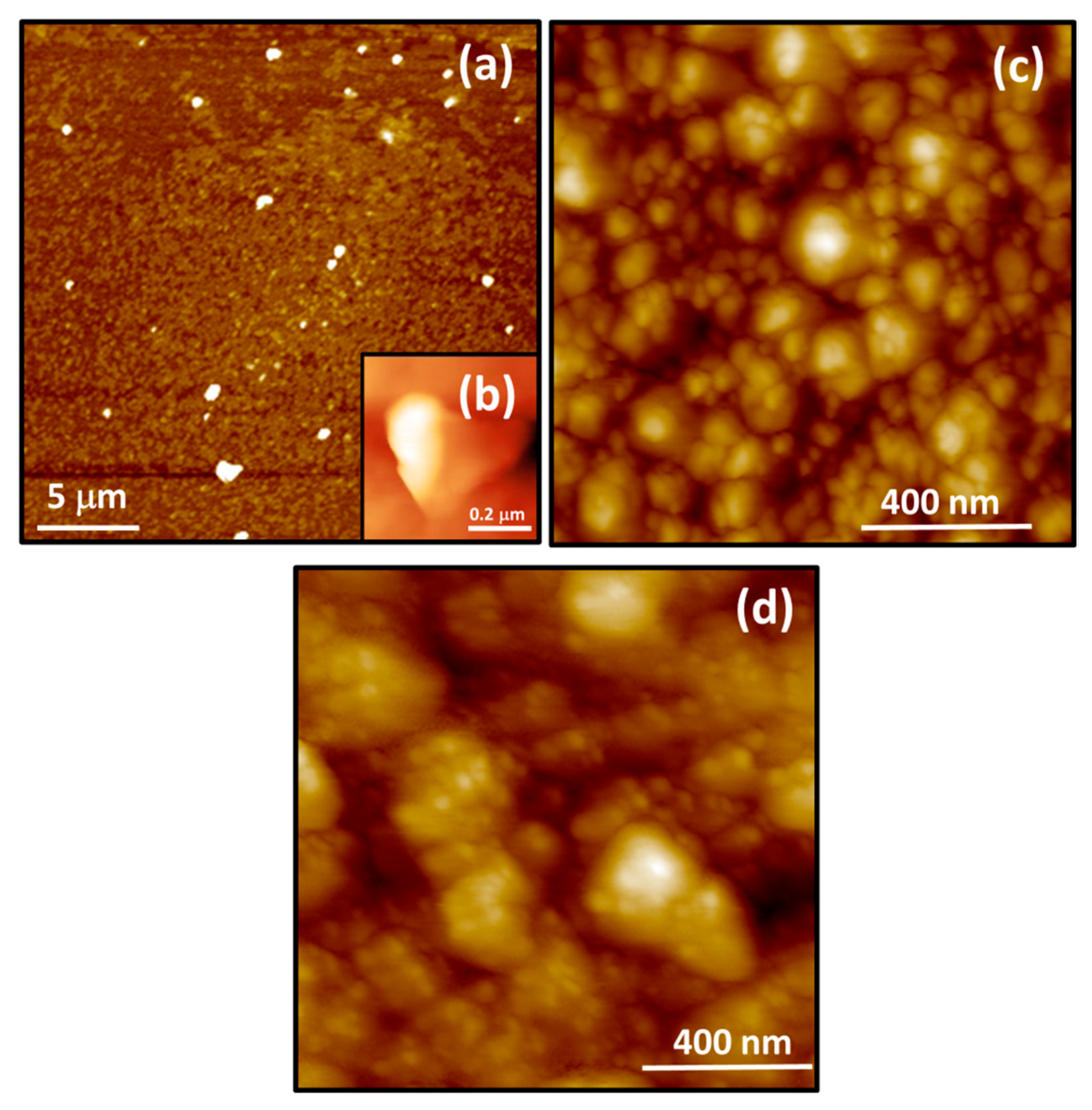
3.2. HR-TEM, SEM and AMF Analyses

Figure 2 shows TEM images of graphene sheets. Multilayer graphene sheets, of several micrometers wide, can be appreciated in Figure 2a, while Figure 2b shows a typical graphene sheet, freely suspended on the copper grid. Figure 2c shows graphene sheets in more detail. It is worth to point out that the obtained graphene shows less structural defects or damages compared with other ones reported in the literature, where chemical treatment with sodium hydroxide, hydrazine or acids mixtures was used [11,12,34]. Figure 3a–c corresponds to TEM images of the ZnO-rGO nanocomposite. These micrographs show several graphene flakes coated homogeneously with ZnO nanoparticles and uniformly anchored on the graphene sheet. Another important characteristic of these images is that there are not nanoparticle aggregations. These results are in agreement with other reports where the nanoparticles were anchored and well dispersed on the surface of graphene sheets [7,20]. The ZnO nanoparticle size was in the range of 5–20 nm (Figure 3b–c). This result may suggest the possibility of obtaining nanocomposites of graphene with other metals, metal oxide nanoparticles or semiconductors. As reported, the uniform distribution of ZnO nanoparticles in graphene sheets can improve the electrical conductivity of the nanocomposite [13].
Figure 4, shows the SEM images the ZnO and ZnO-rGO_3 nanocomposite thin films of samples deposited on soda-lime glass substrates. The micrographs of samples ZnO-rGO_1 and ZnO-rGO_2 are omitted, as their morphology is similar to that of the sample ZnO-rGO_3. It is possible to appreciate that the ZnO thin film (Figure 4a–c) present a grainy texture, with uniform and compact distribution of the grains, which are smaller than those for ZnO-rGO_3. Besides, the ZnO thin film has a relatively smooth morphology, having strong effects on the optical properties, i.e., low transmittance and high absorbance [23]. Conversely, regarding the thin films of ZnO-rGO_3 (Figure 4d–f), the morphology of these films presents significative changes in the size and morphology of the grains. The grains had a “rose-like” structure, with agglomerates nearly 50 nm in size. Size particle in the ZnO-rGO_3 thin-film seems to increase in comparison with ZnO one. Furthermore, the surface grain mean sizes for the obtained films were approximately 20, 50, 70 and 90 nm for ZnO, ZnO-rGO_1, ZnO-rGO_2 and ZnO-rGO_3, respectively.
AFM imaging was used to obtain more information about the surface morphology of ZnO-rGO nanocomposite thin films; Figure 5a,b presents a typical AFM image of graphene flakes; in Figure 5c, the ZnO thin film deposited on soda-lime glass by USP shows a uniform and dense surface; in the same way, in Figure 5d, ZnO-rGO_3 thin film presents a similar morphology, where ZnO nanoparticles have been incorporated graphene flakes and these results are similar getting in TEM micrographs.

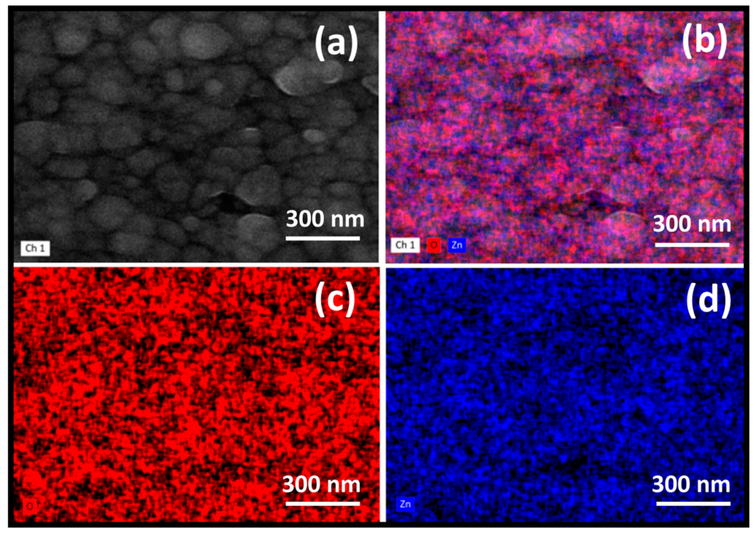
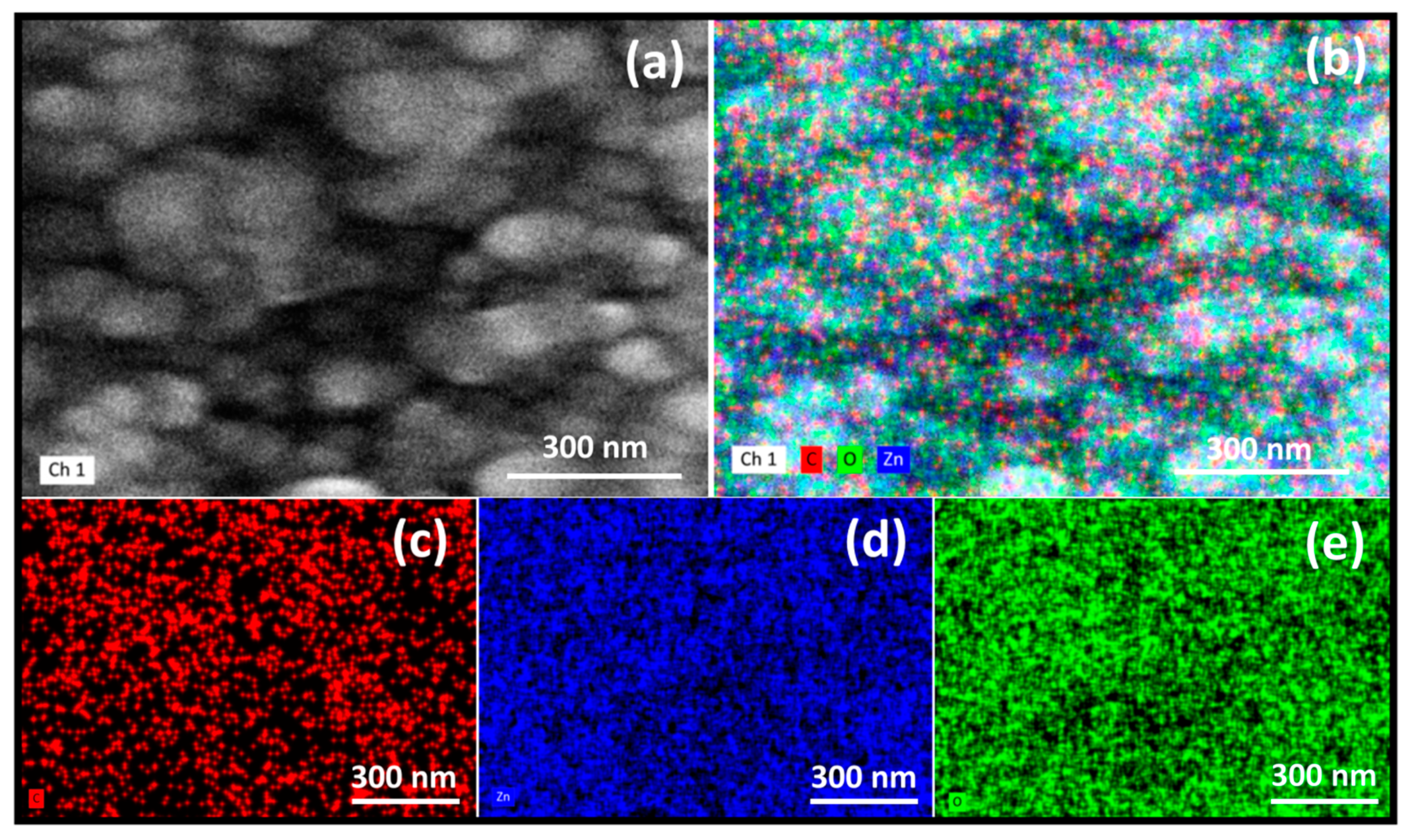
3.3. Elemental Mapping Composition (EDS)

EDS elemental mapping composition of the ZnO and ZnO-rGO_3 nanocomposite thin film is shown in Figure 6 and Figure 7, respectively. The ZnO thin film presented a uniform distribution of Zn and O on the surface of the film (Figure 6a–d), while for the ZnO-rGO_3 thin films a homogeneous distribution of Zn, O and C was determined on the surface of the film (Figure 7a–e), which confirms the expected composition of the nanocomposite. This analysis indicates that the ZnO-rGO nanocomposite thin film can be deposited uniformly by a simple, one-step method.
The atomic percentage of C, Si, O and Zn, as determined by the EDS analyses for the ZnO, ZnO-rGO_1, ZnO-rGO_2 and ZnO-rGO_3 thin films are presented in Table 2. The detection of Si at the ZnO sample is explained by the soda-lime glass substrate. For the ZnO-rGO_1, ZnO-rGO_2 and ZnO-rGO_3 nanocomposite thin films, more Zn than C (graphene) was determined on the surface of the samples. That may be explained by the easier transport of Zn respect to graphene by the USP system when the mixture is deposited on the substrates. For all three samples it was observed that when the thickness of the film increased, the amount of carbon is increased too.

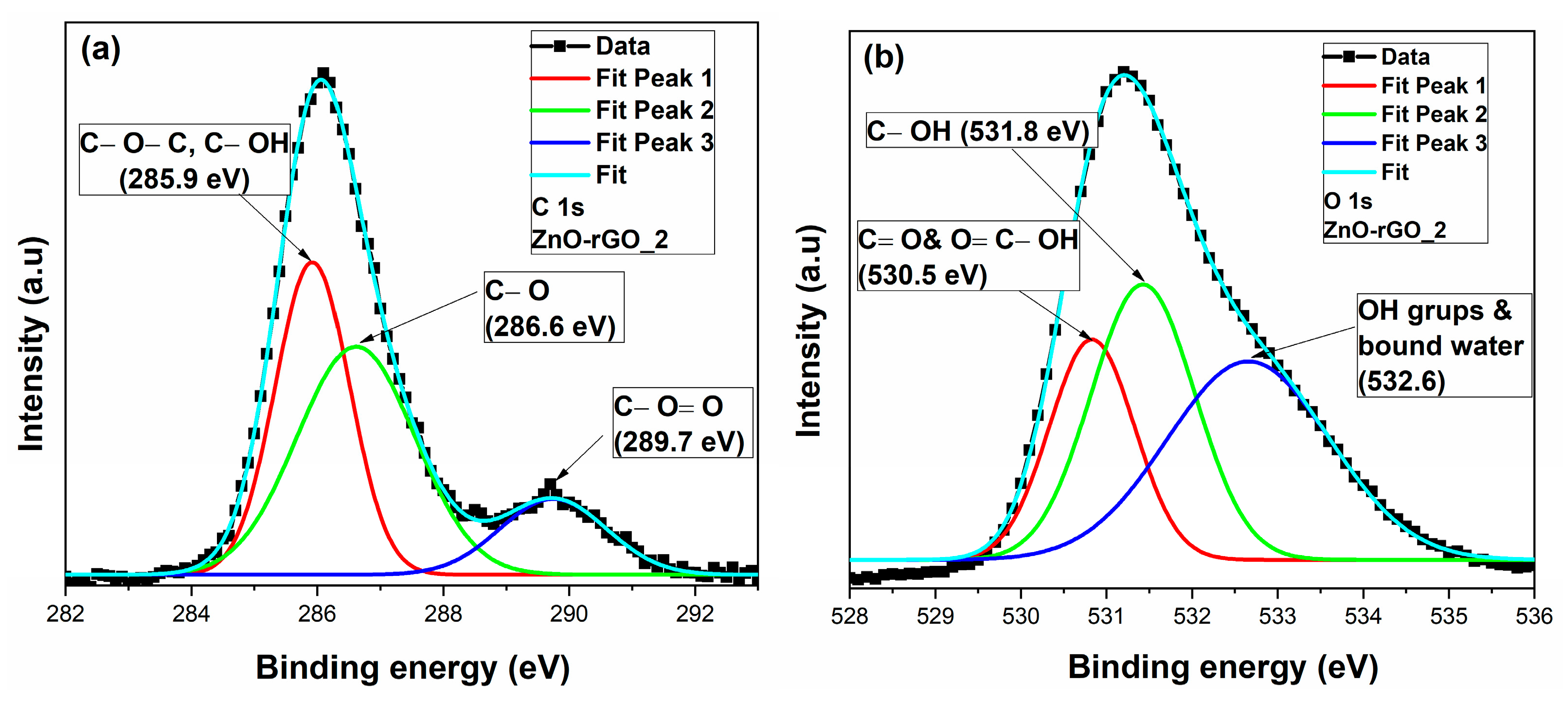
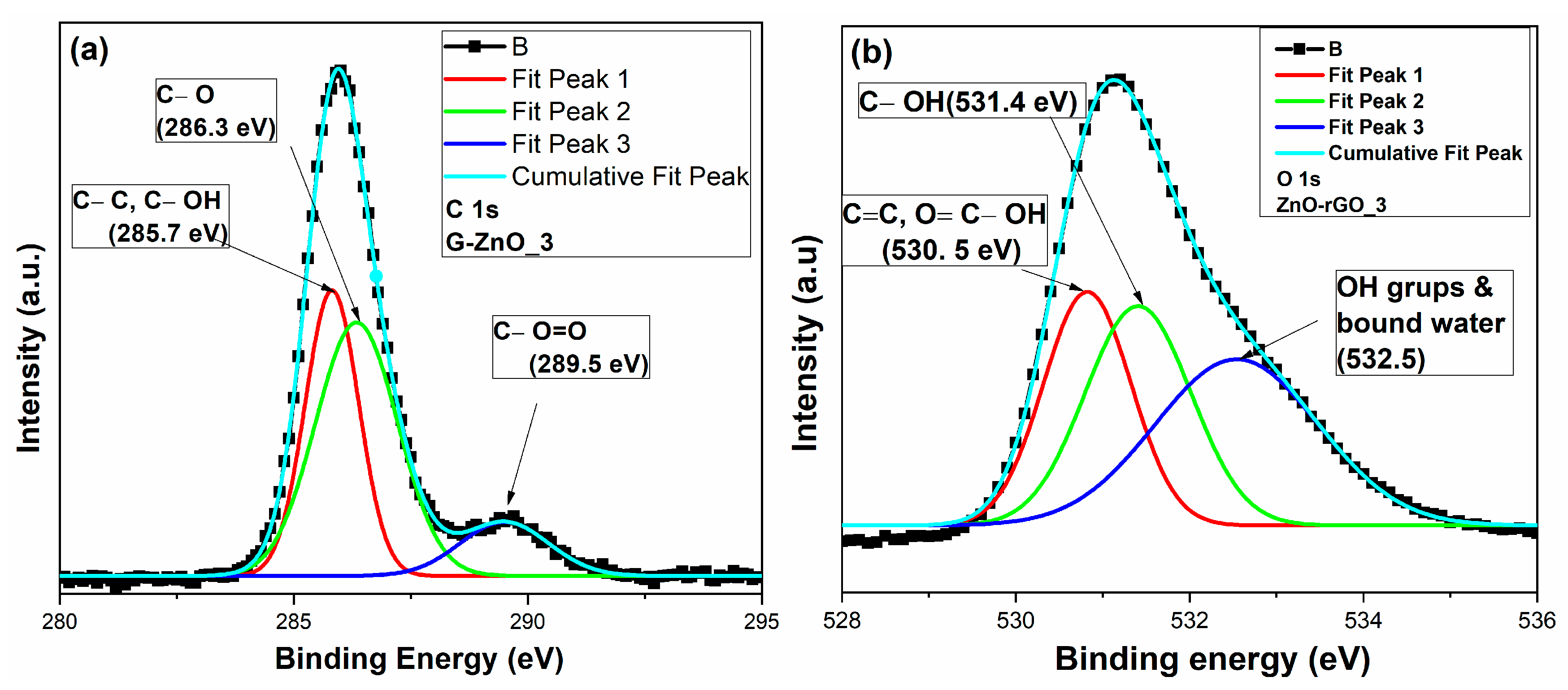
3.4. X-ray Photoelectron Spectroscopy (XPS) Analysis

The XPS spectra of the ZnO and ZnO-rGO_3 thin films (Figure 8a) gives the characteristic peaks of Zn 2p1/2, Zn 2p3/2, O 1s, C 1s, Zn-3s, Zn 3p and Zn 3d with the corresponding binding energies of 1045.2, 1022.9, 532.1, 285.5, 141, 89.7 and 11.9 eV respectively [36]. The high-resolution Zn 2p spectrum for ZnO, ZnO-rGO_2 and ZnO-rGO_3 (Figure 8b) exhibited two significant peaks with binding energies of 1022.1 and 1045.22 eV, corresponding to Zn 2p3/2 and Zn 2p1/2 respectively. The separation of peak energy is 23.2 eV, which confirms the +2 oxidation state of Zn, which is characteristic for the ZnO phase and is in agreement with the literature [36,37]. The intensity of the ZnO spectrum in the ZnO-rGO thin films showed decay in comparison to a pure ZnO thin film. This may be related to the formation of carbon functional groups on the film.
Figure 9 and Figure 10 show the XPS spectrum of the C 1 s and O 1 s bands of ZnO-rGO_2 and ZnO-rGO_3 thin films, in which are presented the O and C, functional groups. On the one hand, analysis of the high-resolution C 1 s spectra using a peak of deconvolution (Figure 9a and Figure 10a), revealed three functional groups around 285.8 eV (C–O–C, C–OH), 286.3 eV (C–O) and 289.1 eV (C–O=O) [38]. On the other hand, the O 1 s spectrum initially appeared at a binding energy of 531.3 eV (Figure 9b and Figure 10b). After its deconvolution, it contained three contributions around 530.8 eV (C=O, O=C–OH), 531.42 eV (C–OH) and 532.66 eV (OH, H2O). The 530.8 eV peak is attributed to the lattice O while the other two components are related to C=O and C–O (sp3) [39]. The assignments of the mentioned functional groups are in agreement with the literature [38,39].
The XPS results, shown in Figure 9 and Figure 10, clearly indicate variations in the oxygen and carbon content for the ZnO_rGO_2 and ZnO_rGO_3 samples. The ZnO_rGO_2 nanocomposite has more oxygen and zinc content than the ZnO_rGO_3 sample, whereas the ZnO_rGO_3 sample has a larger fraction of carbon (graphene). The shifts in the XPS peaks are caused by the charge transfer effect and can be related to changes in the oxidation state of the components in the sample; in this case, the ZnO-rGO_3 thin film presents a lower shift in the binding energy with respect to the ZnO-rGO_2 sample, which suggest it presents a lower oxidation state. Then, there is a reduction of oxygen functional groups in the ZnO-rGO_3 thin film in comparison with ZnO-rGO_2 thin film. This behavior correlates with the deposition temperature. Furthermore, no C–O–Zn peak was found in the nanocomposite thin films indicating that no C–O–Zn bond was formed between the ZnO nanoparticles and the rGO sheets [36].
It is evident from the XPS results, that the ZnO-rGO nanocomposite thin films contain rGO, although no acid was used to obtain GO, as the ZnO-rGO thin films were deposited by the USP method. During the formation of the films, the solution that contains the precursors (Zn and graphene) is a mixture that reacts on a hot substrate (460 °C) to form an oxide film, producing both the rGO and the ZnO that are incorporated into the thin films. The time used to increase the thin film thicknesses is enough for reducing the graphene oxide under the conditions of deposition, forming rGO. It has been reported that the temperature used to deposit the films is low and this is consistent with the electronic device fabrication process [25,40]. This, once again, confirms the presence of rGO in the films, which is similar to the XRD.

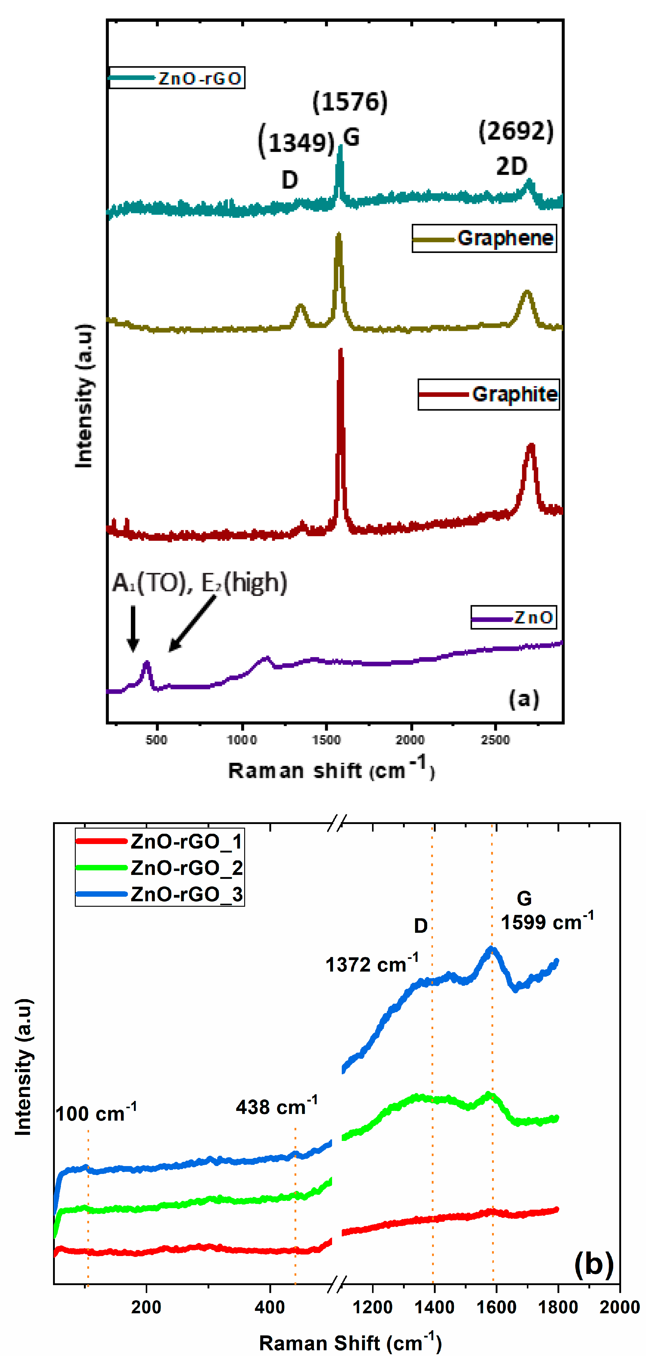
3.5. Raman Spectroscopy

Figure 11a presents the Raman spectra of ZnO, graphite, graphene and ZnO-rGO nanocomposite as ground powders. ZnO exhibits some peaks at 100 cm−1, 438 cm−1 and 379 cm−1, which are attributed to the E2 low, E2 high and A1 (TO) symmetry mode of ZnO [33,39]. E2 (high) was caused by the tensile strain in the films and the vibrations of the oxygen atoms in ZnO lattice [33]. These basic phonon modes are characteristic of the hexagonal wurtzite phase. Moreover, in the same figure, graphite and graphene present three peaks at 1349 cm−1, 1576 cm−1 and 2692 cm−1, which correspond to D, G and 2D bands. It is well-known that the G band is produced by an E2g vibration mode, common to sp2 carbon materials. In contrast, the D band is associated with structural defects related to the disorder-induced vibration of the C–C bond. Finally, the 2D band has been related to the number of layers, which gives a measure of the quality of the produced graphene [36,39].
The Raman spectra for the ZnO-rGO_1, ZnO-rGO_2 and ZnO-rGO_3 thin films are shown in Figure 11b. It is possible to observe that the peaks intensity corresponding to graphene and ZnO decreases. This may be a consequence of the decline of the concentration of G and ZnO into the ZnO-rGO thin films. On the other hand, the intensity of theses peaks is reduced in the nanocomposite due to the interaction of the ZnO and rGO [39]. Therefore, the E2 low and E2 high modes are observed in the Raman spectra, which confirms the formation of hexagonal wurtzite ZnO [41].
Moreover, Figure 11b demonstrates the effect that layer thickness has on the position of the G-band. As the layer thickness increases, the band position shifts to higher energy [42] and the intensity of the G peak increases with the increment of the thickness of the thin films. The G-band observed in the Raman spectrum for graphene powder shows a peak located at 1599 cm−1. These results, confirm the reduction of GO to rGO during the deposition of the films by the USP method due to the substrate temperature [40,43]. This result is in agreement with those obtained from the XRD, SEM, AFM and XPS analyses.
Generally, the intensity ratio of D band and G band (ID/IG) is used to evaluate disorder/defect in G [38,43]. Here, the ID/IG ratio for ZnO-rGO_3 thin films was 0.4. In this case, the G peak of ZnO-rGO_3 thin film was smaller than that for ZnO-rGO powder. That may indicate than the combination of ZnO and GO effectively prevents the restacking of the G layer during the reduction process [38]. The same behavior was observed with pure ZnO, where its characteristic bands in the nanocomposite of the ZnO-rGO_3 films were weaker than in ZnO powder (Figure 11b).

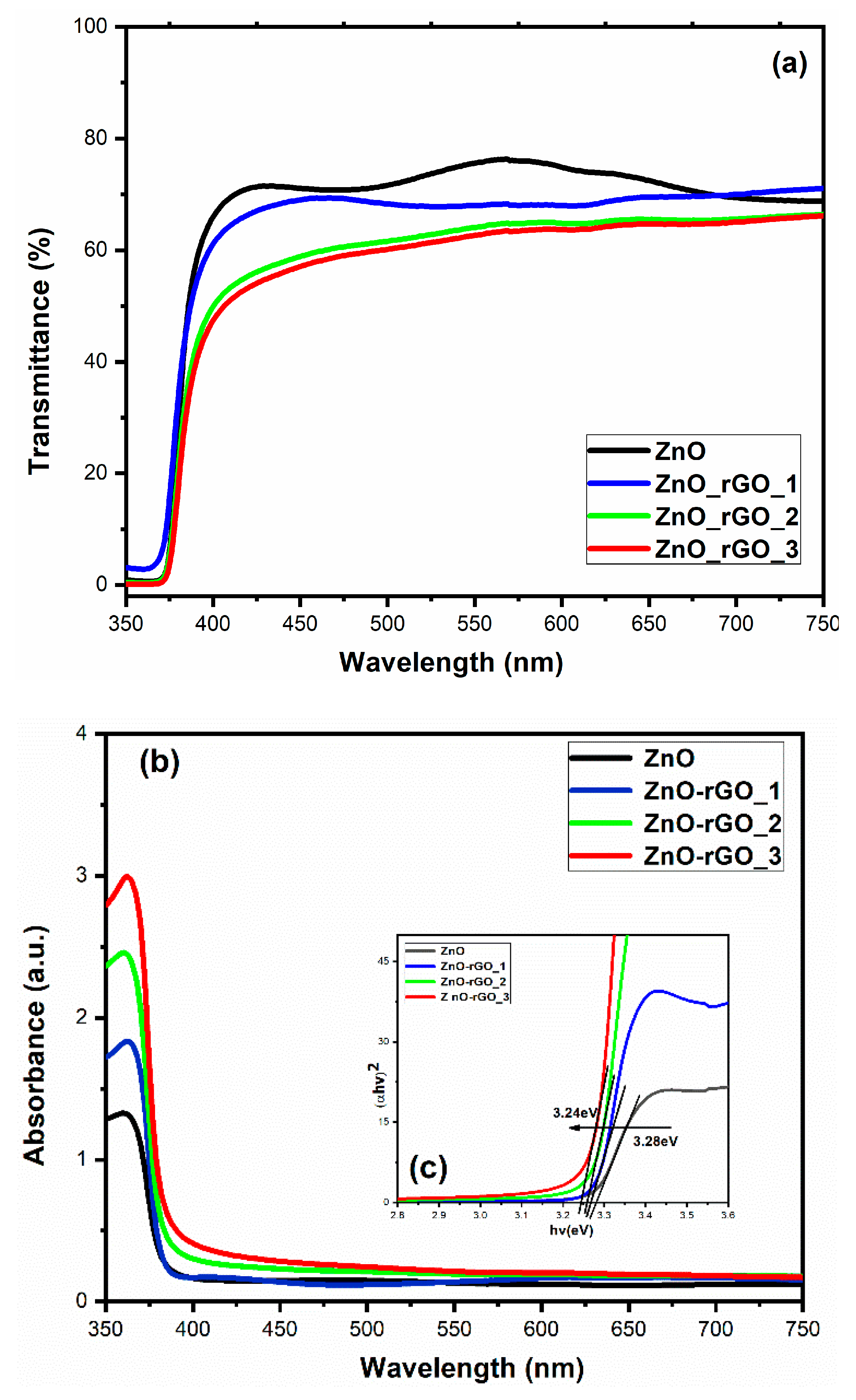
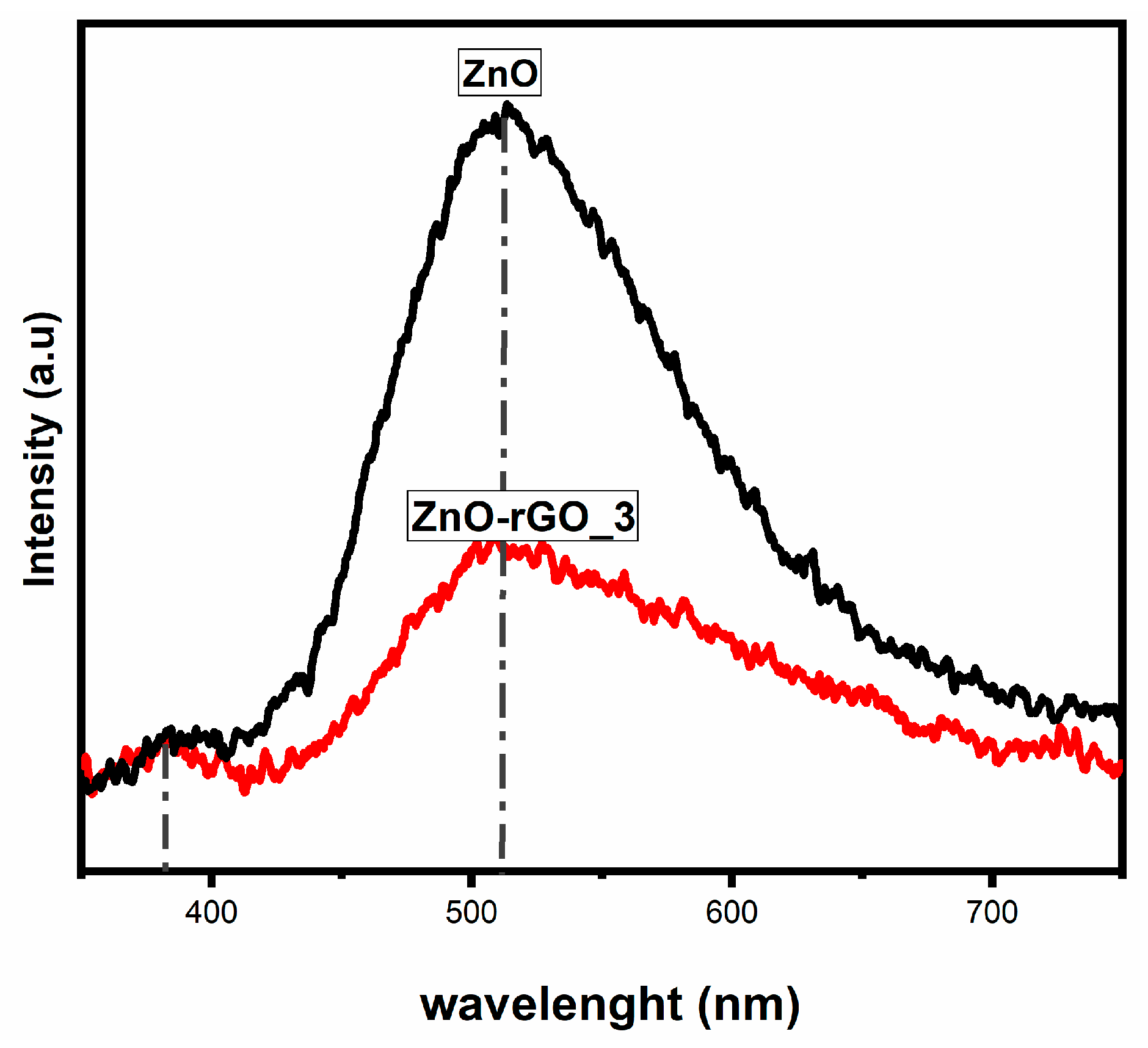
3.6. Optical Measurements

Figure 12 presents the transmittance and absorbance spectra, respectively, for the thin films of ZnO, ZnO-rGO_1, ZnO-rGO_2 and ZnO-rGO_3. Different thickness was analyzed with a UV-visible spectrometer in a wavelength range of 350–750 nm. The transmittance of all thin films was higher than 50% in the visible light region (400–800 nm). These values are in agreement with the values found in the literature [32,37,44]. The transmittance in the ZnO-rGO_2 and ZnO-rGO_3 thin films had values lower than ZnO and ZnO-rGO_1. It is clear that these ZnO-rGO thin films present an increase of the absorbance compared with the ZnO thin film (Figure 12b). This increment of the absorbance in the thin films is related to the increase of surface electric charge of the oxides, which produces an alteration of the electron-hole pair formation during of UV light illumination [44]. Additionally, as the thickness in the films increases with the deposition time, it can produce a greater sensitive area, which generates more electron-hole pairs. These results showed that the formation of the ZnO nanocomposite with GO improves the absorption in the visible-light region [44].
The bandgap energy of ZnO and ZnO-rGO nanocomposite thin films was calculated from the Tauc plot ((α hν)2 versus hν for direct bandgap materials) of its UV-vis absorption spectrum [20]. The bandgap of ZnO, ZnO-rGO_1, ZnO-rGO_2 and ZnO-rGO_3 thin films was estimated from the absorption edge of their respective absorption spectra (Figure 12b). The bandgap values of ZnO, ZnO-rGO_1, ZnO-rGO_2 and ZnO-rGO_3 were estimated at 3.28, 3.26, 3.25 and 3.24 eV, respectively. It indicates that the synthesized thin films could absorb more photons (visible light) than ZnO thin films [34,44]. This behavior is because of the absorbance increases as the film thickness increase due to the deposition time.
Figure 13 compares the relative intensities of the photoluminescence (PL) spectra for the ZnO and the ZnO-rGO_3 nanocomposite thin films. The PL measurements of samples ZnO-rGO_1 and ZnO-rGO_2 were omitted, as their behavior was similar to that of the sample ZnO-rGO_3. It is possible to see a luminescence quenching effect of the ZnO-rGO_3 by about 70% as compared to the ZnO thin film. Degradation of the emission intensity of the ZnO thin film was observed as graphene was incorporated into the nanocomposite. This behavior may be due to interfacial charge transfer from ZnO to graphene, which generates an effective electron transfer, reducing the recombination of photogenerated electron-hole pairs [44,45], and can be more noticeable in ZnO-rGO_3 thin film due to increases in the thickness of the film.
The spectra of ZnO and ZnO-rGO_3 thin films are composed of two main peaks. One peak corresponds to the blue emission at 375 nm and the second peak corresponding to the broad yellow-green band at 436–576 nm [45]. The emission band at 375 nm is due to the electron transition from shallow donor level formed by interstitial Zn atoms to the top of the valence band. The emission band at 511 nm originates from the electron transition from shallow donor level formed by interstitial Zn to shallow acceptor level formed by Zn vacancies [44].

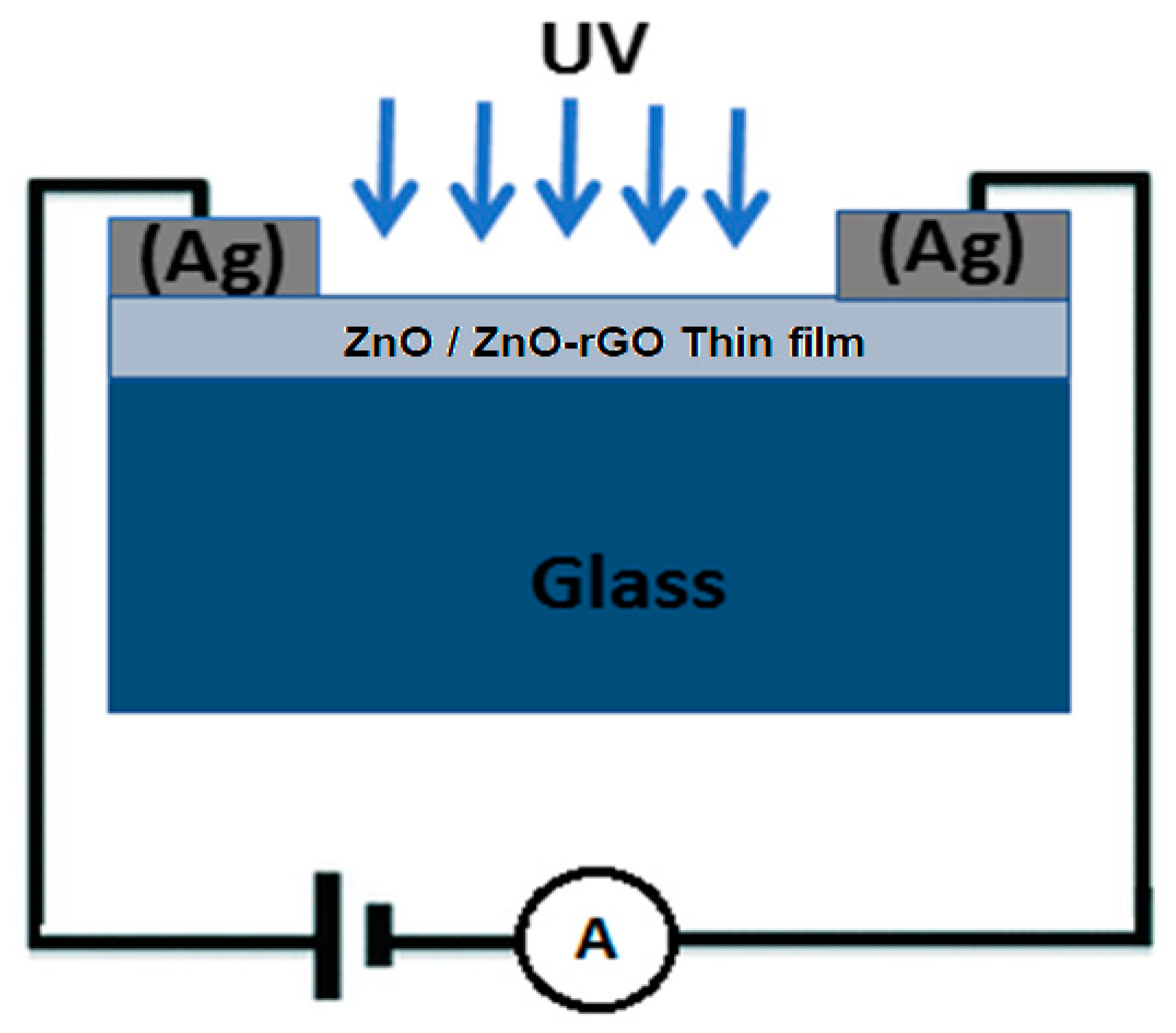
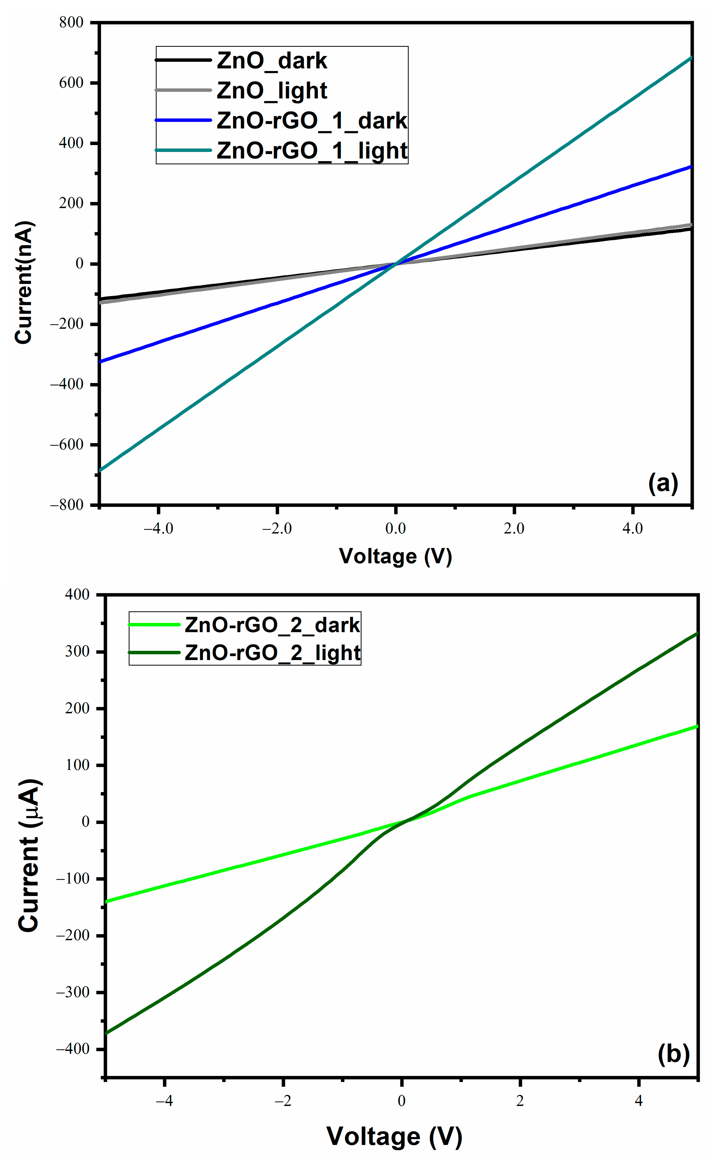
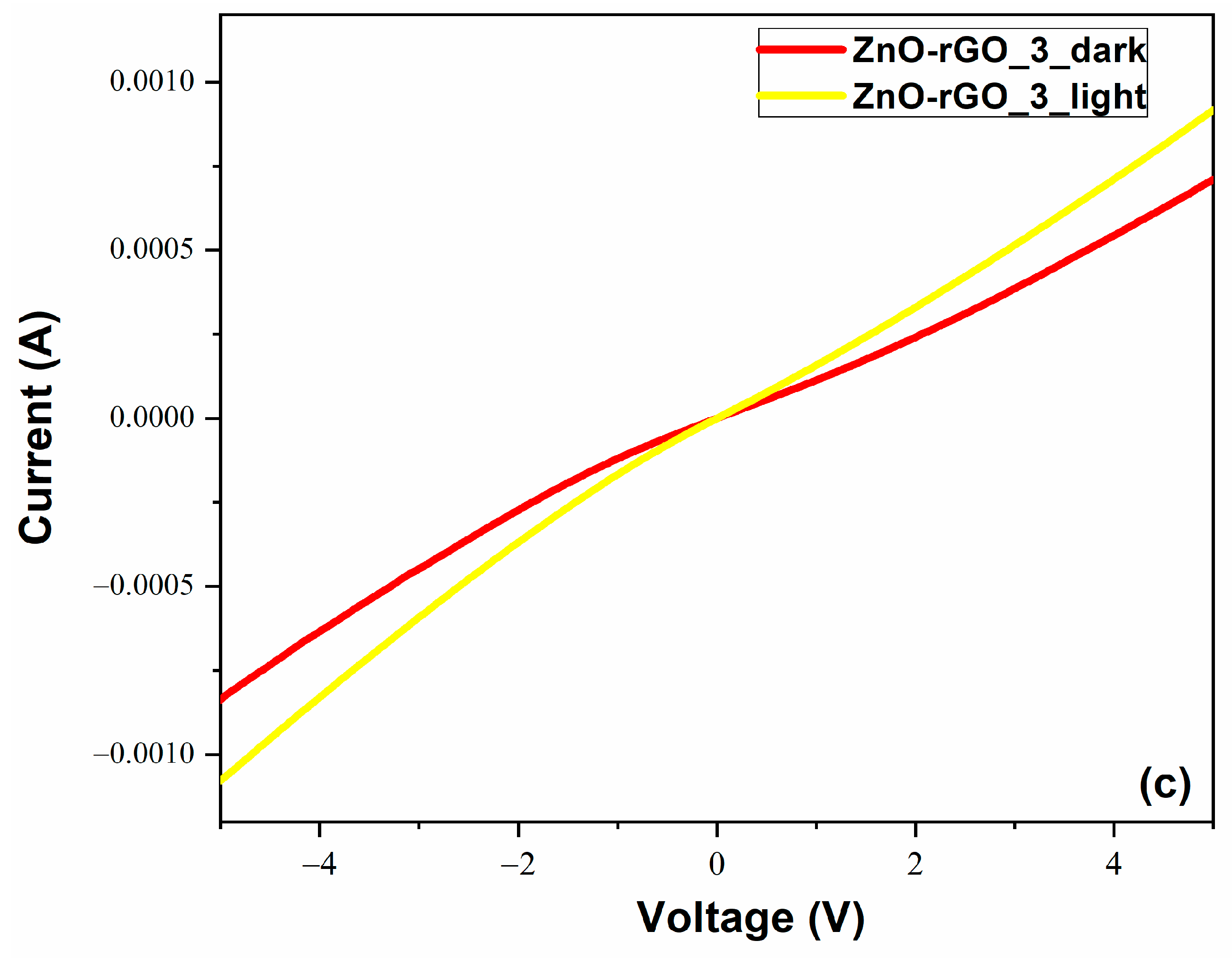
3.7. Electrical Measurements

Figure 14 shows the cross-section of structure used to measure the I–V (current–voltage) curves in the dark and UV light conditions. Figure 15 presents the electrical performance of the ZnO, ZnO-rGO_1, ZnO-rGO_2 and ZnO-rGO_3 nanocomposite thin films. The I–V curves of ZnO-rGO thin films showed an increase in the photocurrent when exposed to the UV illumination compared with the dark condition. Moreover, the photocurrent was higher than pure ZnO thin films. This performance is similar to results previously reported in the literature [4,7,38], and is in agreement with the previously discussed analyses obtained by transmittance, absorbance and PL spectroscopy. As a consequence, it can be suggested that the conductivity of the ZnO thin film improved by the presence of the rGO into the films structure. A reason for this phenomenon is that graphene shows bipolar nature, so it can transfer electrons and holes almost immediately, which can increase the carrier concentration [46].
The I–V curves with UV light of the ZnO and ZnO-rGO_1 structures exhibited a linear I–V characteristic (Figure 15a), indicating the ohmic contact between Ag electrode and films. In contrast, the thicker (ZnO-rGO_2 and ZnO-rGO_3) structures exhibited a non-linear I–V characteristic (Figure 15b,c), suggesting Schottky contact could have formed between the electrode and the thicker films. The resistance of the structure was of 42 MΩ, 15 MΩ, 29 KΩ and 135 Ω in the films of ZnO, ZnO-rGO_1, ZnO-rGO_2 and ZnO-rGO_3, respectively. These results indicate that there is a relation between the resistance of the structure and the thickness of the ZnO-rGO films. When the thickness of the films increased, the resistance of the film decreased and the conductivity increased. This performance could be related mainly to the electronic interaction between carbon atoms and ZnO nanoparticles.
The increased conductivity of ZnO-rGO_1, ZnO-rGO_2 and ZnO_rGO_3 thin films may be attributed to the role of intrinsic defects (i.e., native defects), which are a result of the growth conditions and impurity atoms of the ZnO particles under study. Furthermore, ZnO-rGO is an insulator–semiconductor nanocomposite, where nanoparticles of ZnO are anchored on the surface of insulating rGO sheets. The above means that the mechanism of charge transport in ZnO-rGO nanocomposite is dominated by the fluctuation-induced tunneling (FIT) conduction mechanism [47]. Where ZnO acts like a narrow barrier in an insulating rGO matrix, when the concentration of ZnO is high (there is no rGO), the charge transport is dominated by a hopping conduction mechanism. On the contrary, if the concentration of ZnO decreases, an insulating gap (a small potential barrier) appears between semiconducting ZnO nanoparticles on the rGO surface and the conduction mechanism is now governed by the electrons tunneling across these little barriers separating large conducting regions of ZnO [47,48]. As a consequence, the conductivity of the ZnO-rGO thin films increases when compared to pure ZnO thin films.
In addition, the primary function of the graphene with the ZnO nanoparticles is to increase photodetection. However, there are several intrinsic defects that cause it to reduce this effect. In the dark condition, the oxygen molecules adsorbed on the surface of the thin films capture free electrons; reducing the conductivity of the films. In illumination, photons that have energy higher than the bandgap of ZnO generate electron-hole pairs in the film. Therefore, the holes go to the surface of nanoparticles to be recombined with trapped electrons in O2, thus releasing oxygen from the surface. Therefore, the adsorbed oxygen and the photogenerated holes release the photogenerated electrons, which causes an increase in conductivity of the thin films [49,50].

4. Conclusions

In this study, we successfully grew thin films of the ZnO-rGO nanocomposite. Furthermore, a study of the effect of the thin films thickness on their structural, morphological, optical and electrical properties was performed. XRD, TEM, HRSEM, AFM, XPS and elemental composition analyses, suggest that the USP method produces nanocomposite thin films with a homogeneous coating of ZnO nanoparticles on the graphene surface.
The XRD and Raman results indicate that the nanocomposite thin films incorporate the ZnO nanoparticles into the rGO matrix with a hexagonal wurtzite-type structure, which exhibited its spectroscopic vibrational modes. It was observed that, when the thickness of the thin-film or the graphene amount increased, the PL spectra of the ZnO-rGO nanocomposite thin films decreased. On the other hand, the PL spectra of the nanocomposite thin films increased when the thin film thickness decreased, maybe due to effective inhibition by electron-hole recombination, which enhances its UV detection capability. Variations of the optical absorption of ZnO-rGO thin films decreases with the structure resistance value, as confirmed by I–V measurements of the thin films. These films can transfer electrons and holes almost immediately, which can increase the carrier concentration and therefore the photocurrent.
In addition, graphene flakes were obtained by ultrasonic exfoliation, an alternative, more eco-friendly route instead of the widely used Hummer’s method, which uses toxic and corrosive chemicals. This methodology is cheap and feasible to adopt at any research laboratory.
The physical properties of the prepared ZnO-rGO nanocomposite thin films make them promising for its use as transparent conducting oxides for optoelectronic or photovoltaic applications. The described methodology could be useful for the synthesis of nanocomposites of several metal oxide and different types of G/GO/rGO-based nanomaterials, using a simple one-step process.

Author Contributions

R.R.-A. and S.A.-I. wrote, conceived and designed the experiments; J.A. and A.L.-F., G.F.-C. and Y.P.B. validation, conceptualization, and formal analysis; J.F.C.-V. and J.B.-C. provide resources and systems to work; L.M.-d.l.G. and H.P.M.H. supervision; L.M.-d.l.G., M.Á.M.R., and J.J.G.-A. provide support in review and editing this work. All authors have read and agreed to the published version of the manuscript.

Funding

Raquel Ramírez-Amador acknowledges the financial support CONACYT by a doctoral scholarship support (support: 411956) in the Institute of semiconductor devices program from CIDS-BUAP, as well as VIEP-BUAP financial for support in publication fee.

Acknowledgments

Authors gratefully acknowledge Gabriel Alonso Núñez and Dra. Yasmín Esqueda Barrón (Measurements Raman); Mario H. Farias Sánchez and MC. David Domínguez (XPS measurements); Francisco Ruíz Medina (TEM measurements), José Juan Gervacio Arciniega (AFM measurements); Miguel Ángel Méndez Rojas (Elemental mapping composition-SEM measurement), Mario Moreno Moreno and Netzahualcoyotl Carlos Ramírez (SEM measurements), Javier Martínez Juárez and Dra. Primavera López Salazar (XRD measurements), Ulises Salazar Kuri (Data calculated from DRX), and M.C. Denisse Cortés Salinas (Electrical measurements). Also, the authors would like to thank the facilities given by laboratory equipment of the department of Nanocharacterization of CNyN-UNAM, laboratory equipment of department of electronic of INAOE, Laboratory equipment of CEMMATL of CIDS-ICUAP and the semiconductor laboratory of Ecocampus Valsequillo-CIDS-BUAP.

Conflicts of Interest

The authors declare no conflict of interest with respect to the research.

References

  1. Huang, X.; Qi, X.; Boey, F.; Zhang, H. Graphene-based composites. Chem. Soc. Rev. 2015, 41, 666–686. [Google Scholar] [CrossRef]
  2. Neto, A.C.; Guinea, F.; Peres, N.M.; Novoselov, K.S.; Geim, A.K. The electronic properties of graphene. Rev. Mod. Phys. 2009, 81, 109–162. [Google Scholar] [CrossRef] [Green Version]
  3. Son, D.I.; Kwon, B.W.; Park, D.H.; Seo, W.S.; Yi, Y.; Angadi, B.; Choi, W.K. Emissive ZnO–graphene quantum dots for white-light-emitting diodes. Nat. Nanotechnol. 2012, 7, 465–471. [Google Scholar] [CrossRef] [PubMed]
  4. Manikandan, E.; Kavitha, G.; Kennedy, J. Epitaxial zinc oxide, graphene oxide composite thin-films by laser technique for micro-Raman and enhanced field emission study. Ceram. Int. 2014, 40, 16065–16070. [Google Scholar] [CrossRef]
  5. Zhong, L.; Samal, M.; Yun, K. Synthesis, characterization and electrochemical properties of different morphological ZnO anchored on graphene oxide sheets. Mater. Chem. Phys. 2018, 204, 315–322. [Google Scholar] [CrossRef]
  6. Paul, R.; Gayen, R.N.; Biswas, S.; Bhat, S.V.; Bhunia, R. Enhanced UV detection by transparent graphene oxide/ZnO composite thin films. RSC Adv. 2016, 6, 61661–61672. [Google Scholar] [CrossRef]
  7. Yin, Z.; Wu, S.; Zhou, X.; Huang, X.; Zhang, Q.; Boey, F.; Zhang, H. Electrochemical deposition of ZnO nanorods on transparent reduced graphene oxide electrodes for hybrid solar cells. Small 2010, 6, 307–312. [Google Scholar] [CrossRef]
  8. Teh, S.J.; Yeoh, S.L.; Lee, K.M.; Lai, C.W.; Hamid, S.B.A.; Thong, K.L. Effect of reduced graphene oxide-hybridized ZnO thin films on the photoinactivation of Staphylococcus aureus and Salmonella enterica serovar Typhi. J. Photochem. Photobiol. B Biol. 2016, 161, 25–33. [Google Scholar] [CrossRef]
  9. Wang, H.; Wang, L.; Qu, C.; Su, Y.; Yu, S.; Zheng, W.; Liu, Y. Photovoltaic properties of graphene oxide sheets beaded with ZnO nanoparticles. J. Solid State Chem. 2011, 184, 881–887. [Google Scholar] [CrossRef]
  10. Kwon, B.J.; Kim, J.Y.; Choi, S.M.; An, S.J. Highly transparent and conducting graphene-embedded ZnO films with enhanced photoluminescence fabricated by aerosol synthesis. Nanotechnology 2014, 25, 85701–85707. [Google Scholar] [CrossRef]
  11. Anand, K.; Singh, O.; Singh, M.P.; Kaur, J.; Singh, R.C. Hydrogen sensor based on graphene/ZnO nanocomposite. Sens. Actuators B Chem. 2014, 195, 409–415. [Google Scholar] [CrossRef]
  12. Peng, Y.; Ji, J.; Chen, D. Ultrasound assisted synthesis of ZnO/reduced graphene oxide composites with enhanced photocatalytic activity and anti-photocorrosion. Appl. Surf. Sci. 2015, 356, 762–768. [Google Scholar] [CrossRef]
  13. Saranya, M.; Ramachandran, R.; Wang, F. Graphene-zinc oxide (G-ZnO) nanocomposite for electrochemical supercapacitor applications. J. Sci. Adv. Mater. Devices 2016, 1, 454–460. [Google Scholar] [CrossRef] [Green Version]
  14. Ouyang, Q.; Xu, Z.; Lei, Z.; Dong, H.; Yu, H.; Qi, L.; Chen, Y. Enhanced nonlinear optical and optical limiting properties of graphene/ZnO hybrid organic glasses. Carbon 2014, 67, 214–220. [Google Scholar] [CrossRef]
  15. Jilani, A.; Othman, M.H.D.; Ansari, M.O.; Hussain, S.Z.; Ismail, A.F.; Khan, I.U. Graphene and its derivatives: Synthesis, modifications, and applications in wastewater treatment. Environ. Chem. Lett. 2018, 16, 1301–1323. [Google Scholar] [CrossRef]
  16. Norhayati, H.; Zuhailimuna, M.; Mohd Zobir, H.; Illyas, M.I.; Azmi, M.; Azlan, K.; AdilaMohamad, J. A Brief Review On Recent Graphene Oxide-Based Material Nanoco Mposites: Synthesis And Applications. J. Mater. Environ. Sci. 2016, 7, 3225–3243. [Google Scholar]
  17. Holder, E.; Tessler, N.; Rogach, A.L. Hybrid nanocomposite materials with organic and inorganic components for opto-electronic devices. J. Mater. Chem. 2008, 18, 1064–1078. [Google Scholar] [CrossRef]
  18. Liu, X.; Pan, L.; Lv, T.; Lu, T.; Zhu, G.; Sun, Z.; Sun, C. Microwave-assisted synthesis of ZnO–graphene composite for photocatalytic reduction of Cr (VI). Catal. Sci. Technol. 2011, 1, 1189–1193. [Google Scholar] [CrossRef]
  19. Zhou, X.; Shi, T.; Zhou, H. Hydrothermal preparation of ZnO-reduced graphene oxide hybrid with high performance in photocatalytic degradation. Appl. Surf. Sci. 2012, 258, 6204–6211. [Google Scholar] [CrossRef]
  20. Saranya, M.; Garg, S.; Singh, I.; Ramachandran, R.; Santhosh, C.; Harish, C.; Grace, A.N. Solvothermal preparation of ZnO/graphene nanocomposites and its photocatalytic properties. Nanosci. Nanotechnol. Lett. 2013, 5, 349–354. [Google Scholar] [CrossRef]
  21. Alam, K.; Sim, Y.; Yu, J.-H.; Gnanaprakasam, J.; Choi, H.; Chae, Y.; Sim, U.; Cho, H. In-situ Deposition of Graphene Oxide Catalyst for Efficient Photoelectrochemical Hydrogen Evolution Reaction Using Atmospheric Plasma. Materials 2020, 13, 12. [Google Scholar] [CrossRef] [PubMed] [Green Version]
  22. Rodwihok, C.; Wongratanaphisan, D.; Thi Ngo, Y.L.; Khandelwal, M.; Hur, S.H.; Chung, J.S. Effect of GO Additive in ZnO/rGO Nanocomposites with Enhanced Photosensitivity and Photocatalytic Activity. Nanomaterials 2019, 9, 1441. [Google Scholar] [CrossRef] [PubMed] [Green Version]
  23. Ergin, B.; Ketenci, E.; Atay, F. Characterization of ZnO films obtained by ultrasonic spray pyrolysis technique. Int. J. Hydrogen Energy 2009, 34, 5249–5254. [Google Scholar] [CrossRef]
  24. Bilgin, V.; Kose, S.; Atay, F.; Akyuz, I. The effect of Zn concentration on some physical properties of tin oxide films obtained by ultrasonic spray pyrolysis. Mater. Lett. 2004, 58, 3686–3693. [Google Scholar] [CrossRef]
  25. Akhavan, O. The effect of heat treatment on formation of graphene thin films from graphene oxide nanosheets. Carbon 2010, 48, 509–519. [Google Scholar] [CrossRef]
  26. Qu, W.W.; Jin, W.; Xu, J.Y.; Yang, S.; Peng, J.H. A Theoretical Investigation of the Thermal Decomposition of Zinc Acetate and Zn-Oxo Complex Based on the Pyrolysis Characteristics of the Zinc-Containing Spent Catalyst. Adv. Mater. Res. 2012, 538, 2438–2443. [Google Scholar] [CrossRef]
  27. Mihaiu, S.; Szilágyi, I.M.; Atkinson, I.; Mocioiu, O.C.; Hunyadi, D.; Pandele-Cusu, J.; Toader, A.; Munteanu, C.; Boyadjiev, S.; Pokol, G.; et al. Thermal study on the synthesis of the doped ZnO to be used in TCO films. J. Therm. Anal. Calorim. 2016, 124, 71–80. [Google Scholar] [CrossRef] [Green Version]
  28. Zhuang, H.; Deng, W.; Wang, W.; Liu, Z. Facile fabrication of nanoporous graphene powder for high-rate lithium–sulfur batteries. RSC Adv. 2017, 7, 5177–5182. [Google Scholar] [CrossRef] [Green Version]
  29. Ciszewski, M.; Mianowski, A.; Szatkowski, P.; Nawrat, G.; Adamek, J. Reduced graphene oxide–bismuth oxide composite as electrode material for supercapacitors. Ionics 2015, 21, 557–563. [Google Scholar] [CrossRef] [Green Version]
  30. Yang, S.Y.; Chang, K.H.; Tien, H.W.; Lee, Y.F.; Li, S.M.; Wang, Y.S.; Wang, J.Y.; MA, C.C.M.; Hu, C.C. Design and tailoring of a hierarchical graphene-carbon nanotube architecture for supercapacitors. J. Mater. Chem. 2011, 21, 2374–2380. [Google Scholar] [CrossRef]
  31. Siburian, R.; Sihotang, H.; Raja, S.L.; Supeno, M.; Simanjuntak, C. New route to synthesize of graphene nano sheets. Orient. J. Chem. 2018, 34, 182–187. [Google Scholar] [CrossRef] [Green Version]
  32. Jabeen, M.; Ishaq, M.; Song, W.; Xu, L.; Maqsood, I.; Deng, Q. UV-assisted photocatalytic synthesis of ZnO-reduced graphene oxide nanocomposites with enhanced photocatalytic performance in degradation of methylene blue. ECS J. Solid State Sci. Technol. 2017, 6, M36. [Google Scholar] [CrossRef]
  33. Chen, Y.L.; Hu, Z.A.; Chang, Y.Q.; Wang, H.W.; Zhang, Z.Y.; Yang, Y.Y.; Wu, H.Y. Zinc oxide/reduced graphene oxide composites and electrochemical capacitance enhanced by homogeneous incorporation of reduced graphene oxide sheets in zinc oxide matrix. J. Phys. Chem. C 2011, 115, 2563–2571. [Google Scholar] [CrossRef]
  34. Gong, Y.; Zou, C.; Yao, Y.; Fu, W.; Wang, M.; Yin, G.; Chen, X. A facile approach to synthesize rose-like ZnO/reduced graphene oxide composite: Fluorescence and photocatalytic properties. J. Mater. Sci. 2014, 49, 5658–5666. [Google Scholar] [CrossRef]
  35. Flores-Carrasco, G.; Muñoz-Fernández, L.; Alcántara-Iniesta, S.; Soto-Cruz, B.S.; Milosevic, O.; Rabanal, M.E. Structural and functional properties of ZnO thin films grown on Si substrates by air assisted USP method from non-aqueous solutions at low-temperature. Adv. Powder Technol. 2017, 28, 93–100. [Google Scholar] [CrossRef]
  36. Haldorai, Y.; Voit, W.; Shim, J.J. Nano ZnO@ reduced graphene oxide composite for high performance supercapacitor: Green synthesis in supercritical fluid. Electrochim. Acta 2014, 120, 65–72. [Google Scholar] [CrossRef]
  37. Longo, A.; Verucchi, R.; Aversa, L.; Tatti, R.; Ambrosio, A.; Orabona, E.; Maddalena, P. Graphene oxide prepared by graphene nanoplatelets and reduced by laser treatment. Nanotechnology 2017, 28, 224002. [Google Scholar] [CrossRef]
  38. Kumar, N.; Srivastava, A.K.; Patel, H.S.; Gupta, B.K.; Varma, G.D. Facile synthesis of ZnO–reduced graphene oxide nanocomposites for NO2 gas sensing applications. Eur. J. Inorg. Chem. 2015, 11, 1912–1923. [Google Scholar] [CrossRef]
  39. Posa, V.R.; Annavaram, V.; Koduru, J.R.; Ammireddy, V.R.; Somala, A.R. Graphene-ZnO nanocomposite for highly efficient photocatalytic degradation of methyl orange dye* under solar light irradiation. Korean J. Chem. Eng. 2016, 33, 456–464. [Google Scholar] [CrossRef]
  40. Sengupta, I.; Chakraborty, S.; Talukdar, M.; Pal, S.K.; Chakraborty, S. Thermal reduction of graphene oxide: How temperature influences purity. J. Mater. Res. 2018, 33, 4113–4122. [Google Scholar] [CrossRef]
  41. Samuel, M.; Koshy, J.; Chandran, A.; George, K.C. Optical phonon confinement in ZnO nanorods and nanotubes. Indian J. Pure Appl. Phys. 2010, 48, 703–708. [Google Scholar]
  42. Radoń, A.; Włodarczyk, P.; Łukowiec, D. Structure, temperature and frequency dependent electrical conductivity of oxidized and reduced electrochemically exfoliated graphite. Phys. E Lowdimens. Syst. Nanostruct. 2018, 99, 82–90. [Google Scholar] [CrossRef]
  43. Yadav, R.; Kumar, V.; Saxena, V.; Singh, P.; Singh, V.K. Two-step synthesis of reduced graphene oxide with columnar-shaped ZnO composites and their photocatalytic performance with natural dye. J. Aust. Ceram. Soc. 2019, 1, 1–12. [Google Scholar] [CrossRef]
  44. Gayathri, S.; Jayabal, P.; Kottaisamy, M.; Ramakrishnan, V. Synthesis of ZnO decorated graphene nanocomposite for enhanced photocatalytic properties. J. Appl. Phys. 2014, 115, 173504. [Google Scholar] [CrossRef]
  45. Boukhoubza, I.; Khenfouch, M.; Achehboune, M.; Mothudi, B.M.; Zorkani, I.; Jorio, A. Graphene oxide/ZnO nanorods/graphene oxide sandwich structure: The origins and mechanisms of photoluminescence. J. Alloys Compd. 2019, 797, 1320–1326. [Google Scholar] [CrossRef]
  46. Shuai, W.; Hu, Y.; Chen, Y.; Hu, K.; Zhang, X.; Zhu, W.; Lao, Z. Composite structure of ZnO films coated with reduced graphene oxide: Structural, electrical and electrochemical properties. J. Semicond. 2018, 39, 23001–23006. [Google Scholar] [CrossRef]
  47. Jilani, S.M.; Gamot, T.D.; Banerji, P. Thin-film transistors with a graphene oxide nanocomposite channel. Langmuir 2012, 28, 16485–16489. [Google Scholar] [CrossRef]
  48. Qu, G.; Fan, G.; Zhou, M.; Rong, X.; Li, T.; Zhang, R.; Chen, D. Graphene-Modified ZnO Nanostructures for Low-Temperature NO2 Sensing. ACS Omega 2019, 4, 4221–4232. [Google Scholar] [CrossRef] [Green Version]
  49. Al-Fandi, M.; Oweis, R.; Albiss, B.A.; AlZoubi, T.; Al-Akhras, M.A.; Qutaish, H.; Al-Shawwa, E. A prototype ultraviolet light sensor based on ZnO nanoparticles/graphene oxide nanocomposite using low temperature hydrothermal method. In IOP Conference Series: Materials Science and Engineering; IOP Publishing Ltd.: Irbid, Jordan, 2015; Volume 92, p. 012009. [Google Scholar] [CrossRef] [Green Version]
  50. Yang, T.; Sun, B.; Ni, L.; Wei, X.; Guo, T.; Shi, Z.; Duan, L. The mechanism of photocurrent enhancement of ZnO ultraviolet photodetector by reduced graphene oxide. Curr. Appl. Phys. 2018, 18, 859–863. [Google Scholar] [CrossRef]
Scheme 1. Schematic representation for the preparation ZnO-rGO nanocomposite thin films.
Crystals 10 00073 sch001
Scheme 2. Illustration of the diagram of ultrasonic spray pyrolysis (USP) system.
Crystals 10 00073 sch002
Figure 1. X-ray diffraction patterns. (a) Graphite and graphene oxide in powder and (b) ZnO and ZnO-rGO thin films.
Crystals 10 00073 g001
Figure 2. TEM images of graphene sheets in solution obtained by sonication: (a) multilayer, (b) several sheets and (c) an individual few-layered sheet.
Crystals 10 00073 g002
Figure 3. TEM images of (a) ZnO-rGO nanocomposite, (b) ZnO nanoparticles anchored on the edge of graphene sheets and (c) ZnO nanoparticles anchored into graphene sheets.
Crystals 10 00073 g003
Figure 4. SEM micrographs of ZnO and ZnO-rGO_3 films at different scale (1 µm, 500 nm and 300 nm). (a–c) ZnO and (d–f) ZnO-rGO_3.
Crystals 10 00073 g004
Figure 5. Atomic force microscopy (AFM) micrographs of (a,b) graphene sheets; (c) ZnO and (d) a ZnO-rGO_3 thin film.
Crystals 10 00073 g005
Figure 6. Elemental mapping analysis of a ZnO thin film: (a) specific area, (b) ZnO, (c) O and (d) Zn.
Crystals 10 00073 g006
Figure 7. Elemental mapping analysis of a ZnO-rGO_3 thin film: (a) specific area, (b) C, O and Zn, (c) C, (d) Zn and (e) O.
Crystals 10 00073 g007
Figure 8. XPS (a) survey spectra of ZnO and ZnO-rGO_3 and (b) Zn 2p spectrum for ZnO, ZnO-rGO_2 and ZnO-rGO_3.
Crystals 10 00073 g008
Figure 9. XPS spectrum of ZnO-rGO_2 thin film: (a) deconvolution C 1 s and (b) deconvolution O 1s.
Crystals 10 00073 g009
Figure 10. XPS spectrum of ZnO-rGO_3 thin film: (a) deconvolution C 1 s and (b) deconvolution O 1 s.
Crystals 10 00073 g010
Figure 11. Raman Spectra of (a) ZnO, graphite, graphene and ZnO-rGO in powder, and (b) ZnO-rGO thin films.
Crystals 10 00073 g011
Figure 12. Optics measurement of ZnO and ZnO-rGO thin films, (a) transmittance spectra, (b) absorbance spectra and (c) the inset confirmed the band gap estimation.
Crystals 10 00073 g012
Figure 13. Photoluminescence spectra of ZnO and ZnO-rGO_3.
Crystals 10 00073 g013
Figure 14. Diagram of ZnO and ZnO-rGO thin film to measure I–V curves in dark and with UV light.
Crystals 10 00073 g014
Figure 15. Measurement I–V (current–voltage) curves in dark and with UV light thin films of (a) ZnO and ZnO-rGO_1, (b) ZnO-rGO_2 and (c) ZnO-rGO_3.
Crystals 10 00073 g015aCrystals 10 00073 g015b
Table 1. Structural parameters of ZnO and ZnO-rGO thin films.
SampleTd
(min)
Thicknesses
(nm)
Position of (002)
Peak (°)
B (°)
(Broading or
Half Width)
Crystallite
Size (nm)
R(%)
ZnO2 13034.600.50616.0(1)8.96
ZnO-rGO_1 215034.390.57716.3(1)9.76
ZnO-rGO_2 3.525034.310.55017.2(2)9.29
ZnO-rGO_3 5 37034.440.54517.5(1)9.91
Table 2. Energy dispersive spectroscopy (EDS) analysis of ZnO and ZnO-rGO thin films.
SampleConcentration
Atom
(%)
Si C OZn
ZnO5.10049.8145.00
ZnO-rGO_102.9643.4552.77
ZnO-rGO_208.5731.4260.01
ZnO-rGO_3013.7927.5858.62

