Article

Effect of Zn Doping in CuO Octahedral Crystals towards Structural, Optical, and Gas Sensing Properties

1
Functional Materials and Energy Devices Laboratory, Department of Physics and Nanotechnology, SRM IST, Kattankulathur Tamil Nadu 603 203, India
2
Graduate School of Science and Technology, Shizuoka University, Hamamatsu 432 8011, Japan
3
Research Institute of Electronics, Shizuoka University, Hamamatsu 432 8011, Japan
4
Technical Physics Division, Bhabha Atomic Research Center, Mumbai 400 085, India
*
Author to whom correspondence should be addressed.
Crystals 2020, 10(3), 188; https://doi.org/10.3390/cryst10030188
Submission received: 17 February 2020 / Revised: 5 March 2020 / Accepted: 7 March 2020 / Published: 9 March 2020
(This article belongs to the Section Crystalline Materials)

Abstract

:
Monodispersed CuO octahedral crystals were successfully synthesized using a low-temperature co-precipitation method. Zinc doping in CuO created surface defects that enhanced oxygen adsorption on the surface crucial for gas sensing applications. Pure and Zn-doped CuO sensor films were realized using the doctor blade method. The sensor films showed selective response towards a low concentration of NO2 at a lower operating temperature of 150 °C. Doping with Zn causes the resistance of the sensor film to decrease due to the enhancement of charge carriers with an analogous improvement in the sensor response. The observed decrease in sensor resistance agreed well with the findings of the work function studies. Zinc doping resulted in an increase in work function by 180 meV which, after NO2 exposure, was found to increase by a further 130 meV, attributed to the oxidizing behavior of the test gas.

Graphical Abstract

1. Introduction

Cupric oxide (CuO) is the most widely studied oxide of all other copper oxides. Other copper suboxides, such as Cu2O and Cu2O3, are not stable materials [1]. Copper oxide is a p-type semiconductor and has many notable properties like antibacterial capability, high stability, and ease of use. It has been utilized in numerous applications including photocatalysis, supercapacitors, lithium ion batteries, infrared photo detectors, biosensors, and gas sensors [2,3,4,5,6,7,8]. It is an ideal absorber material for solar cells, as its optical absorption edge lies in the range between 1.2 eV and 1.9 eV [9,10]. It is an excellent sensing material. For example, Yang et al. [7] synthesized CuO nanorods using hydrothermal method and investigated the gas sensing response towards organic vapors. Similarly, Wang et al. [8] reported reducing volatile organic sensing via sol-gel-synthesized CuO nanoparticles. It has been synthesized using numerous techniques such as hydrothermal, physical vapor deposition, sputtering, chemical vapor deposition, and co-precipitation methods [4,6,11]. Among these, the co-precipitation method using the water bath technique, in particular, has the benefit of low-temperature growth, low cost, and a simple process [12]. It has been demonstrated that by doping transition metals into the semiconductor matrix, electrical, optical, and functional properties can be improved [13,14,15,16]. Importantly, doping improves the gas sensing characteristics, as it provides more defect states followed by adsorption and desorption of oxygen species [17]. Among all transition metals, Zn causes more effective doping, as it has comparable ionic radii with Cu2+ and possesses the same oxidation states [18,19,20].
Nitrogen dioxide is one of most highly toxic gases and a major air pollutant in the environment. It is usually generated from industrial waste, automobile by-products, fossil fuel burning, cigarette smoke, and power plants. It is responsible for acid rain due to the fact of its interaction with water molecules present in the atmosphere [21,22]. When the concentration of NO2 is higher than 20 ppm, it may lead to immediate distress and cause death. Hence, it is desirable to detect NO2 at lower concentrations so that the timely preventive and precautionary measures can be taken to ensure better human health and environments.
Accordingly, in the present work, Zn-doped CuO octahedral crystals were synthesized using the water bath process. The Zn-doping effects in CuO octahedral crystals towards structural, optical, and electrical properties were investigated in detail. The sensor films showed selective response towards low concentrations of NO2 at lower operating temperatures of 150 °C. A sensing mechanism is proposed based on gas sensing and work function studies.

2. Experimental Procedure

2.1. Chemicals

Polyvinylpyrrolidone (PVP), copper sulfate pentahydrate (CuSO4·5H2O), zinc sulfate heptahydrate (ZnSO4·7H2O), dextrose (C6H12O6), sodium carbonate (Na2CO3), and trisodium citrate dihydrate (Na3C6H5O7·2H2O) were purchased from Wako Pure Chemical Industries Limited, Japan. All the chemical reagents were of analytical reagent (AR) grade and used directly as received without further purification.

2.2. Synthesis Procedure

The preparation of CuO octahedral crystals was carried out using the water bath process [23]. Sixty milliliters of DI water solution containing 4.5 gram of PVP, 0.653 gram of Na3C6H5O7·2H2O, 0.382 gram of Na2CO3, 0.757 gram of C6H12O6, and 34 mM CuSO4·5H2O were prepared. The solution was mixed by vigorous stirring at 1000 rpm for 30 min at room temperature resulting in a light blue solution with a pH value of 10. The solution was kept at 70 °C in a thermostatic water bath for 2 h. After the reaction, brick red Cu2O crystal precipitates were obtained. It was repeatedly washed with DI water and ethanol and collected by centrifugation followed by drying at 60 °C for 12 h. For synthesizing Zn-doped Cu2O octahedral crystals, ZnSO4·7H2O was mixed in starting solution with different molarities. Pure and Zn-doped CuO films were prepared by coating as-synthesized samples on a cleaned glass substrate using the doctor blade coating method followed by annealing at 450 °C for 2 h in air. The film thickness of the prepared samples was measured using cross-sectional SEM analysis and was found to be ~30 µm for all the prepared samples. The samples were labeled as P for pristine CuO; and S1, S2, S3, S4, S5, and S6 for Zn-doped CuO samples with increasing Zn concentrations of 0.34 mM, 1.02 mM, 1.7 mM, 3.4 mM, 6.8 mM, and 17 mM, respectively.

2.3. Sample Characterizations

The XRD studies were carried out on a RINT2200 X-ray diffractometer (XRD) (Rigaku Corporation, Tokyo, Japan) with a Cu-Kα radiation source (λ = 1.54 Å). Raman measurements were performed using a JASCO NRS-7100 instrument (JASCO Corporation, Tokyo, Japan) with an incident green laser having an excitation wavelength of 532 nm. Photoluminescence (PL) studies were done at room temperature using JASCO-FP8600 instrument (JASCO Corporation, Tokyo, Japan). The morphology and the structural characterization were performed with a JEOL JSM-7001F field emission scanning electron microscopy (FESEM) (JEOL Limited, Tokyo, Japan) at an accelerating voltage of 15 kV. Compositional analysis and elemental mapping were performed using energy-dispersive X-ray spectroscopy (EDS) (EDAX APOLLO X) (AMETEK Co. Limited, Tokyo, Japan). Elemental qualitative analysis was performed by X-ray photoelectron spectroscopy (XPS) (Shimadzu Axis Ultra DLD) (Shimadzu Corporation, Kyoto, Japan). Crystallographic properties, such as defects and d-spacing, were measured by transmission electron microscope (TEM) (JEOL JEM 2100F) (JEOL Limited, Tokyo, Japan) with an accelerating voltage of 200 kV.

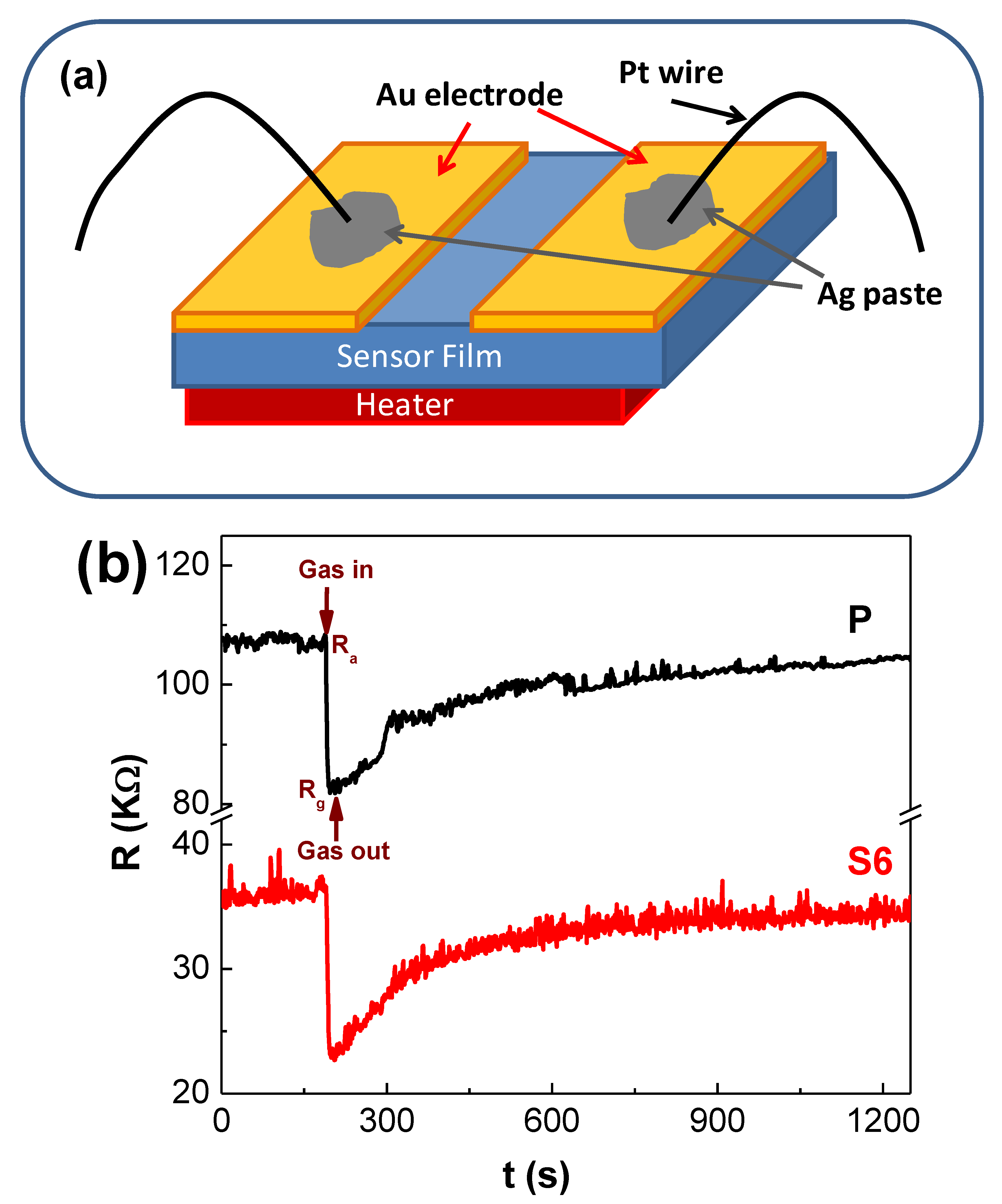
2.4. Gas Sensing Measurements

For gas sensing studies, electrode contacts were realized by depositing a 120 nm thick gold layer with 500 µm separation using a thermal evaporation method. Final electrical connections were taken with Pt wires and silver paint as shown schematically in Figure 10a. The gas sensing study was performed on a table-top static gas sensing setup as described elsewhere [24,25]. Sensor films were then fixed in an airtight gas sensing chamber. Test gas was injected in the chamber with the required concentration of test gas using a gas-tight syringe. The sensor response (S) was calculated from the response curves:
S   ( % ) = R a R g R a × 100 ,   for   oxidizing   gases
S   ( % ) = R g R a R a × 100 ,   for   reducing   gases
where Ra and Rg are resistances of the sensor film in air and test gas, respectively.

2.5. Work Function Measurements

For work function measurement, pure and Zn-doped CuO films were coated on conducting an indium–tin oxide (ITO) substrate using the doctor blade method. The contact potential difference (CPD) measurements of the prepared films were carried out by a scanning Kelvin probe technique (SKP) system using a surface photovoltage (SPV) module (SKP5050 with SPV020 module, KP Technologies Ltd., UK) as described elsewhere [26,27]. From the CPD, the work function (in meV) was measured:
ϕ = 5100 CPD Au + CPD sample meV ,
where 5100 is the work function of gold in meV, CPDAu is the CPD between the tip and the gold-coated reference sample, and CPDsample is the CPD between the tip and the sample. All the measurements were performed at room temperature. The average value of CPD was measured by raster scanning of the tip across the sample surface of a 4 mm2 area (scan). To elucidate the effect of gas exposure on sensor films, work function measurements were performed by exposing the sensor to 50 ppm of NO2 at 150 °C with subsequent quenching to room temperature.

3. Results and Discussion

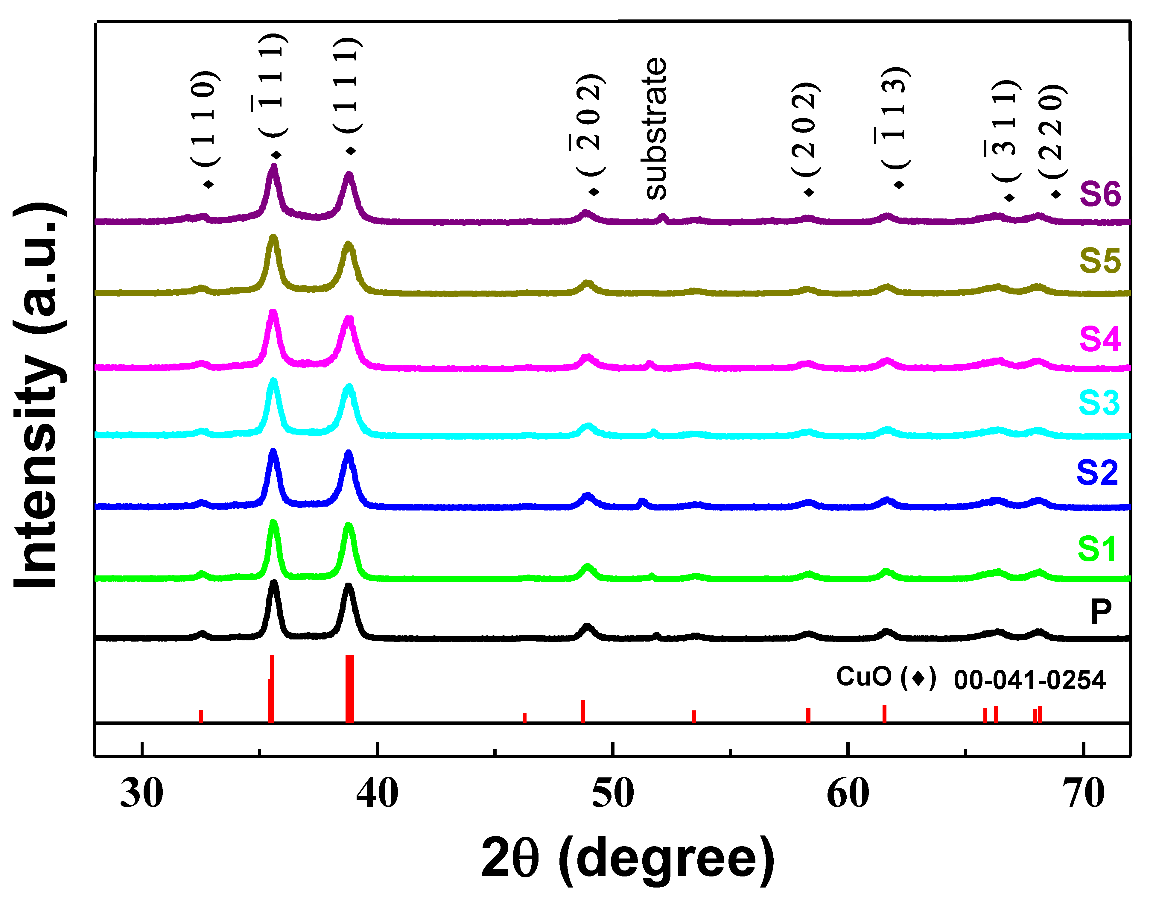
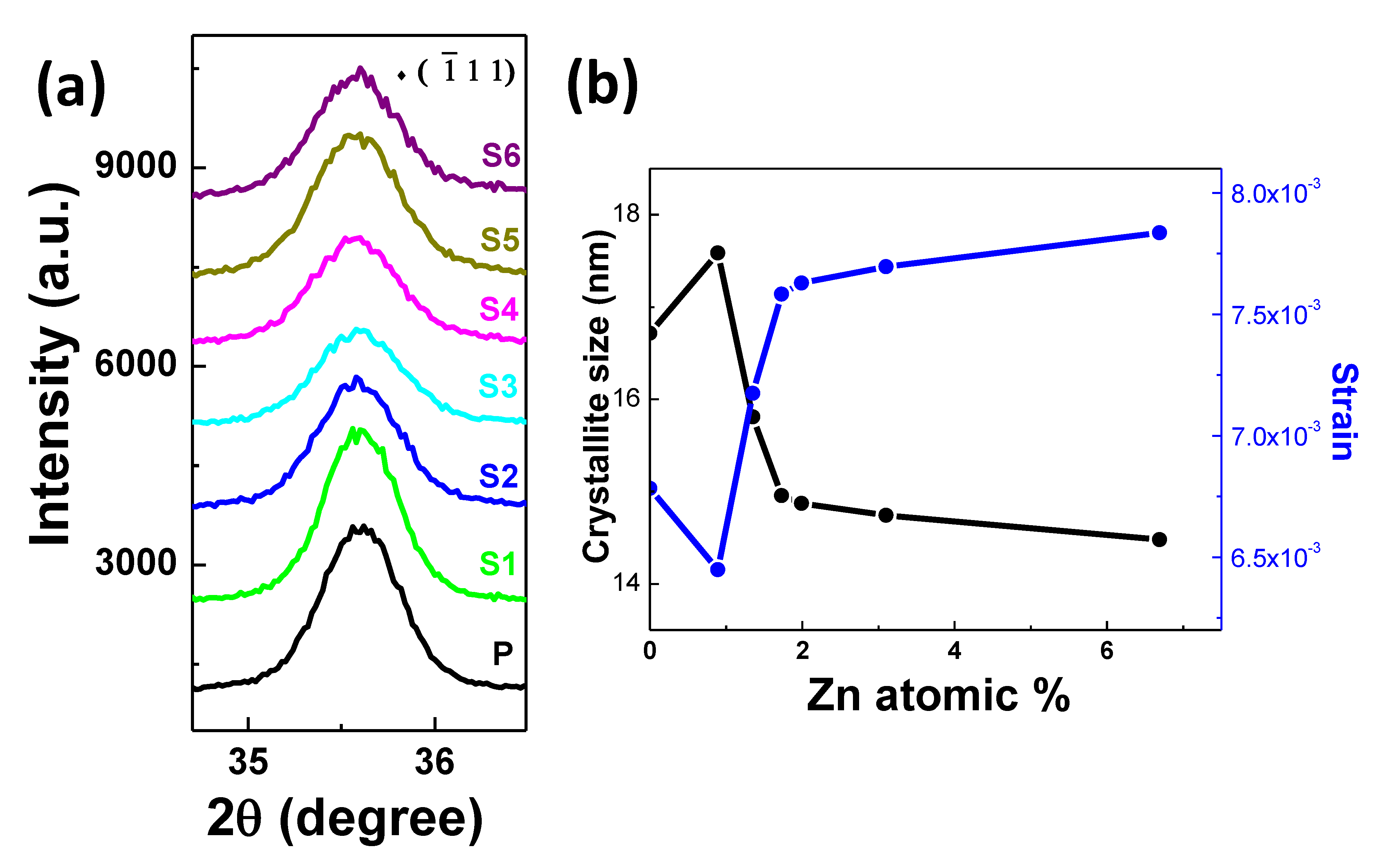
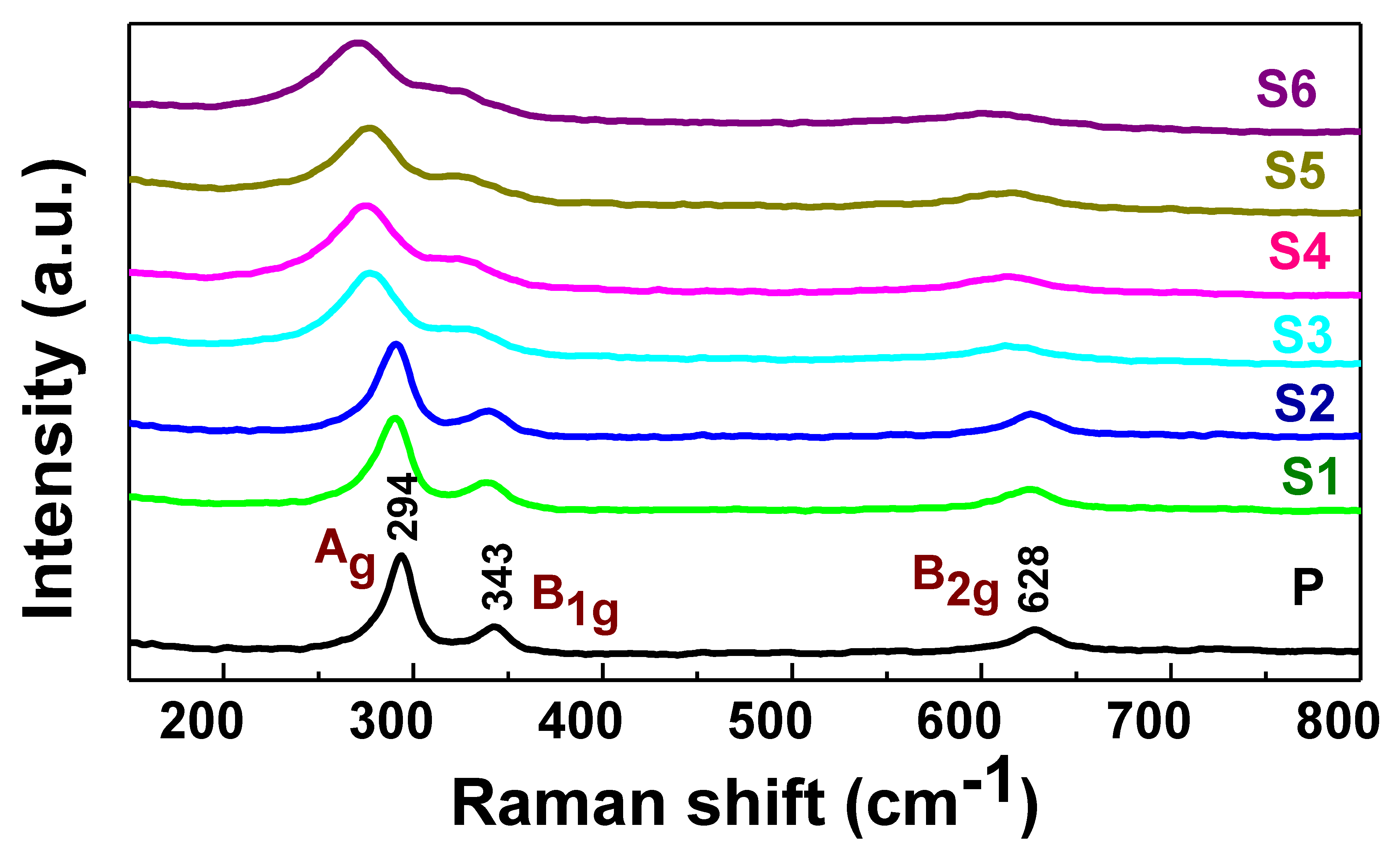
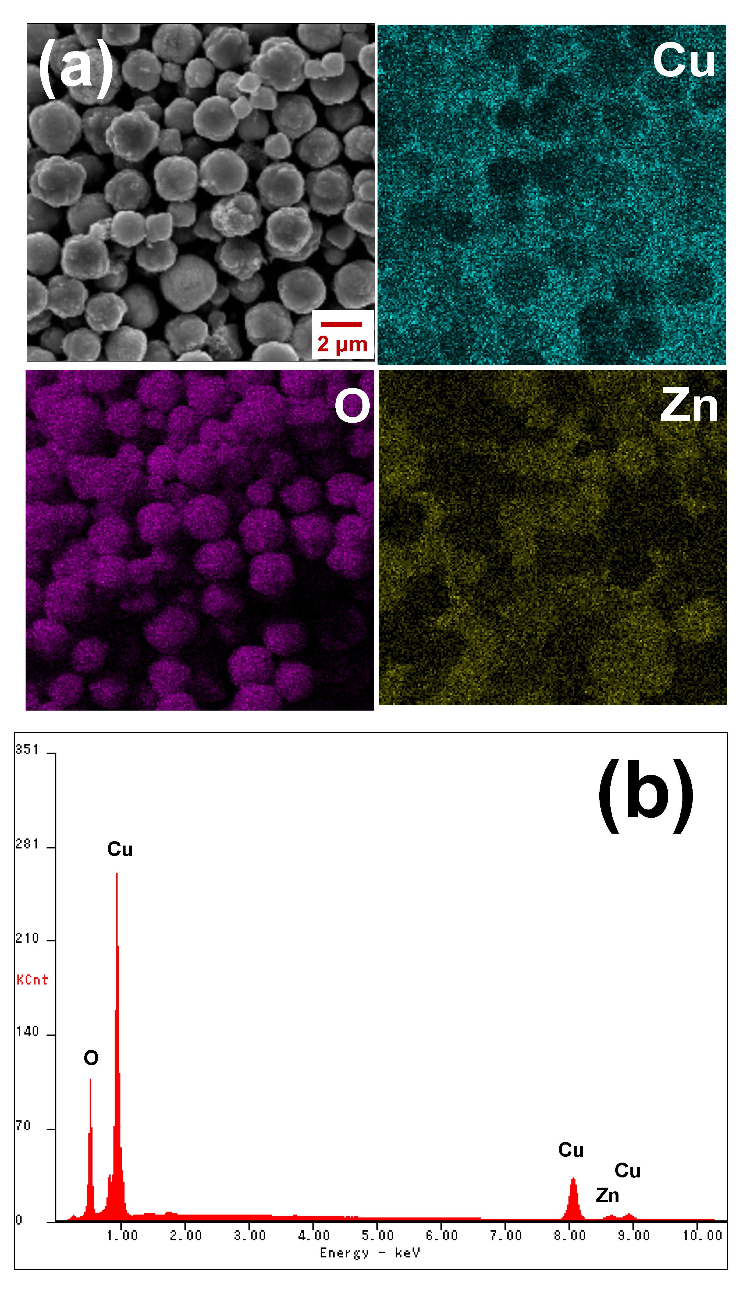
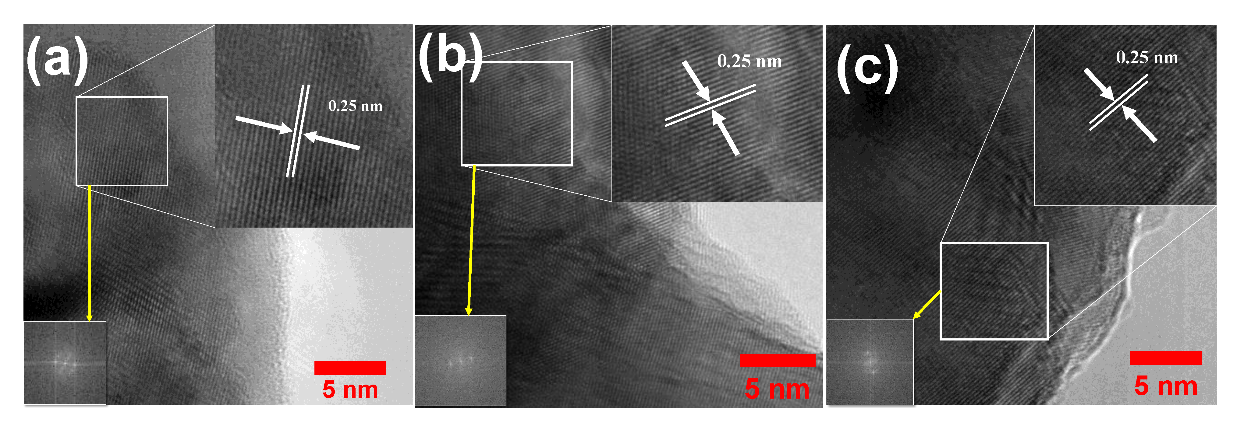
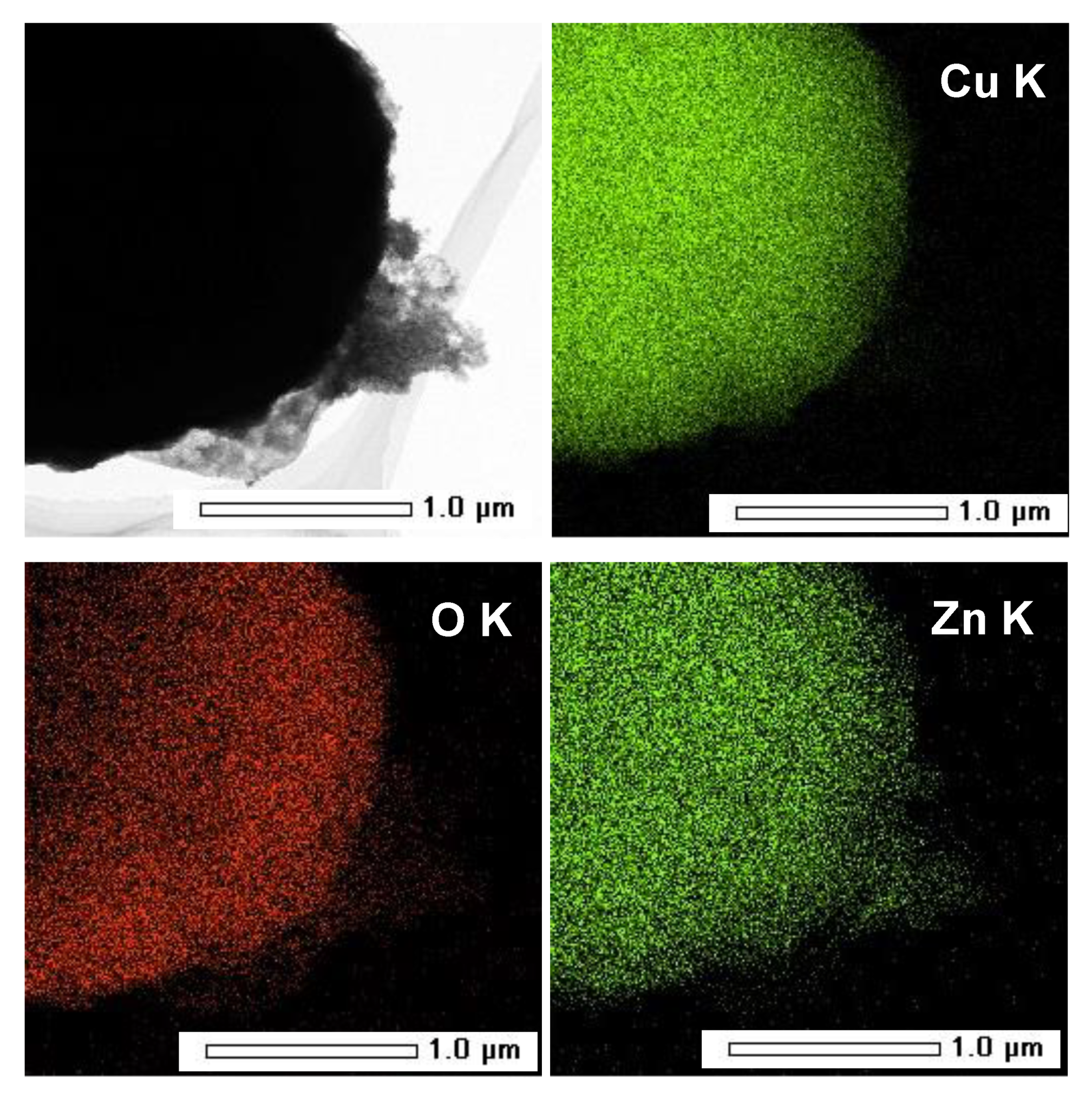
3.1. Structural and Morphological Characterization

As shown in Figure 1, the XRD patterns for pure and Zn-doped CuO films indicated the pure phase formation of CuO without any impurity peaks related to Zn or its suboxides. This can be attributed to the good dispersion of Zn2+ ions on the sites of Cu2+ ions in the CuO matrix [20,28,29]. The XRD patterns could be well indexed with monoclinic CuO (JCPDS file No. 00-041-0254) with ( 1 ¯ 1 1) and (1 1 1) major planes with a space group symmetry of C2/c. Further, the diffraction peak broadening indicates that the synthesized samples had a crystallite size in the nanometer range. Interestingly, the shift of diffraction angle (2θ) along major the ( 1 ¯ 1 1) planes as a function of doping in Zn-doped CuO films were observed which suggests the substitution of Zn ions in place of Cu ions (Figure 2a). This is attributed to the tensile stress which results in the shift to a lower angle [19]. The d-spacing values for samples P, S1-S6 were calculated using Bragg’s law and found to be 0.252 ± 0.0001 nm which further suggests successful substitution of Zn ions on the sites of Cu ions in CuO lattice. The crystallite size was evaluated for ( 1 ¯ 1 1) peak of all the samples using Scherrer formula [29]:
D = K   λ β   Cos   θ ,
where K = 0.9 is the shape factor, D is the average crystallite size, λ is the wavelength of the incident X-ray beam (0.15406 nm), β is the full width and half maxima value, and θ is the diffraction angle.
Further the effective strain in the films was calculated using Williamson–Hall (W–H) equation [30]:
ε = β 4   tan   θ ,
The Zn doping concentration’s dependence on average crystallite size and strain were calculated and are shown in Figure 2b. Crystallite size was found to be decreased, while strain was increased for high Zn doping. At lower Zn concentrations, crystallite size increased, and strain decreased which led to lattice distortion by anisotropic shrinkage of lattices due to the stress [14,19]. Maximum crystallite size and minimum strain were observed to be 17.6 nm and 6.4 × 10⁻³, respectively, for sample S1. Zinc ions provided the strain in the lattice which hindered the growth of the CuO crystal, resulting in the reduction in crystallite size. Strain was found due to the low activation energy, so ions could transfer from trap sites to nucleation sites resulting in smaller crystallite sizes. Further, the Zn dopant atomic percentages were estimated using EDS analysis and are shown in Table 1.
The Raman spectra of pure and Zn-doped CuO films with different Zn concentrations are presented in Figure 3. The primitive cells of monoclinic CuO contain two molecular units, and therefore there are 12 vibrational modes: three acoustic modes (Au + 2Bu), six infrared active modes (3Au + 3Bu), and three Raman active modes (Ag + 2Bg) [29]. Due to the site symmetry, only oxygen atom displacements contribute to active Raman modes. The Raman spectra of pure CuO films showed Raman vibration at 294 cm−1, 343 cm−1, and 628 cm−1 corresponding to Ag, B1g, and B2g, respectively. A slight change in the wave number could be assigned to the size and crystallinity effect [29,31]. No extra peak was observed after Zn doping which confirms that there was no new phase formation which is consistent with the XRD results. Figure 3 confirms the continuous red-shift and the peak broadening of the Ag phonon mode with an increase in the Zn dopant concentration. This is attributed to a reduction in particle size and defects due to the strain after doping [29,31,32,33]. A red shift in the Raman spectra confirms the tensile strain [34] which is the cause of a size reduction and is in accordance with the XRD results (Figure 2b). There were not many differences observed in XRD patterns and Raman spectra for the Zn-doped samples (S1 to S6); therefore, for further investigations, samples P, S3, and S6 are only considered.
The structural morphologies and sizes of Zn-doped CuO crystals deposited on glass substrate were investigated using FESEM and are depicted in Figure 4. The FESEM images show the uniform growth of monodispersed CuO octahedral crystals. From the SEM images, after doping with Zn, the shapes of the particles were converted from octahedral to diffused spherical structures with a reduction in the granular nature with an increase in Zn concentration owing to tensile strain (Figure 2 and Figure 3) [34].
The chemical composition of pure and Zn-doped CuO films were analyzed using EDS. The elemental atomic percentages of the pure and Zn-doped CuO films are presented in Table 1 for all the prepared samples. The atomic percentage of Zn was found to increase as the doping concentration increased, but it was very less compared to the Zn molarity which was used in the starting solution. This was due to the different solubility limits and reaction kinetics of Zn compared to Cu. The sample S6 showed a higher atomic percentage of oxygen (~41%) species compared to other samples (~31%). The EDS elemental mapping showed the uniform distribution of Zn, Cu, and O atoms for sample S6 (Figure 5a). The EDS spectra for sample S6 showed peaks corresponding to Cu, Zn, and O elements (Figure 5b).
Transmission electron microscopy (TEM) analysis was performed to check the morphological changes, defects, and d-spacings for the samples. The TEM images for samples P, S1, and S6 showed a polycrystalline nature as shown in Figure 6. For the measurement of the d-spacing value, the major plane ( 1 ¯ 1 1) in CuO crystals were confirmed using fast Fourier transformation (FFT) fitting. The d-spacings for samples P, S1, and S6 were found to be equal, i.e., 0.25 nm, as like the XRD results. There was no significant change in the d-spacing after Zn doping attributable to the doping of Zn ions inside the CuO lattice without disturbing the crystal structure [19]. Elemental mapping was recorded using EDS equipped with scanning transmission electron microscopy (STEM) at higher magnification to check atomic distribution in Zn-doped CuO particles. Figure 7 shows the STEM image and elemental distribution for sample S6. It is evident that Cu, Zn, and O atoms were distributed uniformly in the sample.
The XPS study was performed to confirm the formation of CuO and Zn doping in the octahedral crystals. The whole spectrum was calibrated by a C1s peak at 284.8 eV [35]. The Cu 2p spectra (Figure 8a) present two peaks corresponding to Cu 2p1/2 and Cu 2p3/2 at 952.4 eV and 932.6 eV, respectively, with two shake-up satellites at higher binding energy sides, shown with arrows, which are characteristics of Cu (II) in its oxide form [26,36]. After Zn doping, Cu 2p peaks were shifted to a higher binding energy side as compared with those of pure CuO particles. Higher electronegativity of Zn (1.372) as compared to that of Cu (1.336) caused lowering of the electron density around the central Cu ion by introducing oxygen and thereby results in a blue shift [37,38,39]. In the O 1s spectra, three major peaks in the range of 529 eV to 534 eV were assigned to the lattice oxygen (OL), oxygen in the crystal matrix at the oxygen-deficient site (OV), and surface adsorption oxygen (OS), respectively [40]. As shown in Figure 8b, after Zn doping, the O1s peak also shifted to the higher binding energy side, like Cu 2p. For a higher concentration of Zn doping (i.e., in the case of sample S6), a separate oxygen peak was observed. It corresponded to the adsorbed oxygen species present on the surface [41]. The Zn 2p (Figure 8c), for the Zn-doped CuO films, was identified by the two characteristic peaks at 1045.1 eV and 1021.9 eV corresponding to 2p1/2 and 2p3/2, respectively [42,43].

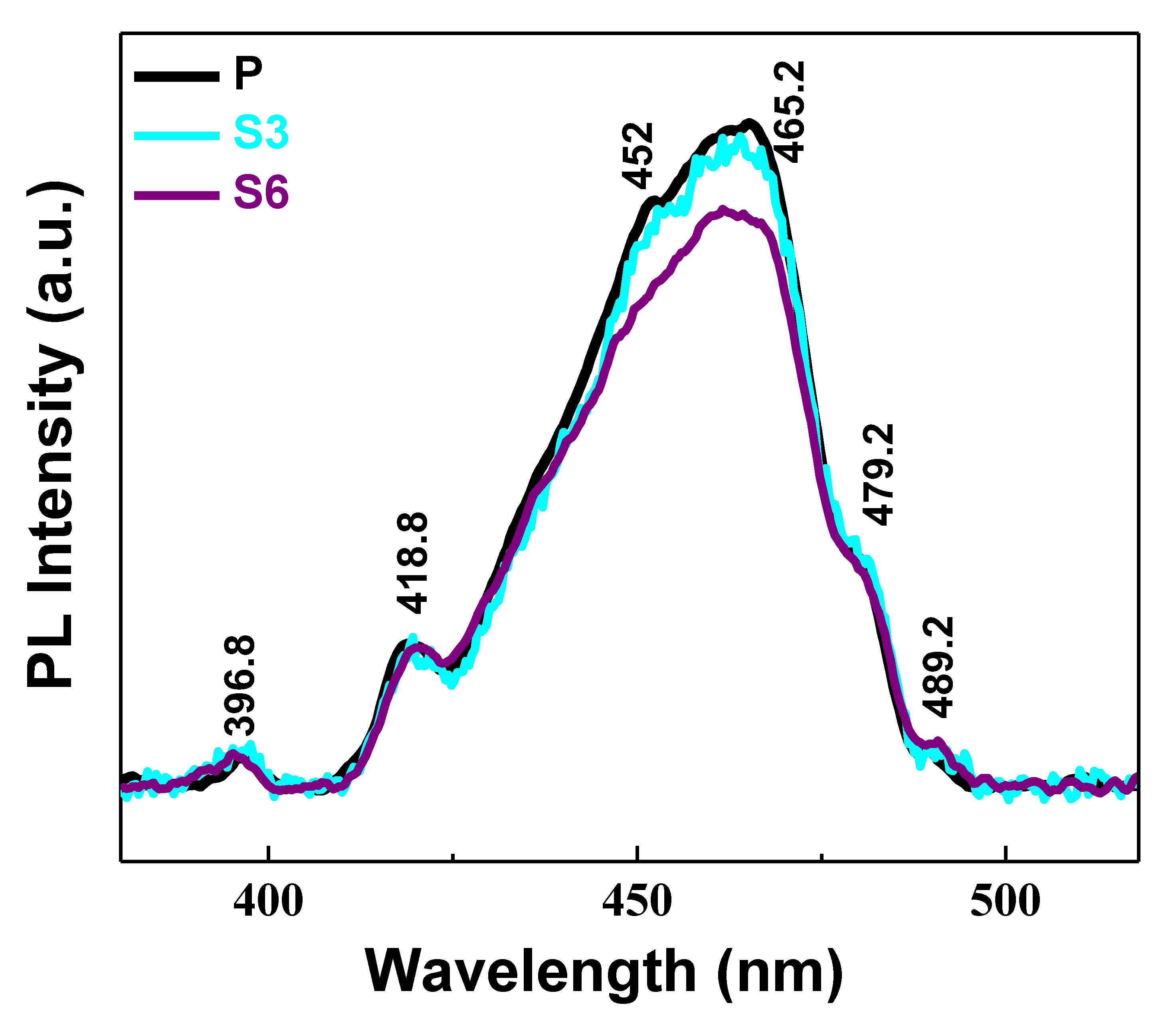
3.2. Optical Studies

The influence of Zn doping on CuO films regarding the intrinsic and extrinsic defects were investigated by photoluminescence (PL) spectra recorded in the wavelength range of 380–520 nm and is shown in Figure 9. The spectrum showed emission peaks at 396.8 nm, 418.8 nm, 452.0 nm, 465.2 nm, and 479.2 nm for pristine CuO film. The PL peak between 450 and 475 nm is attributed to the intrinsic defects or surface states in CuO [44]. After Zn doping in CuO, the peak at 452 nm disappeared and emission intensity were found decreased with change in slope of PL curves. The decrease in intensity is attributed to the lattice distortions, defects and reduction in crystallinity [45]. The PL intensity of the Zn-doped CuO films was lower than that of the pure CuO crystals, indicating the suppression of electron–hole recombination [46]. This is attributed to the increment of charge carriers (holes) after Zn doping in CuO; this evident of the enhancement of the adsorbed oxygen species.

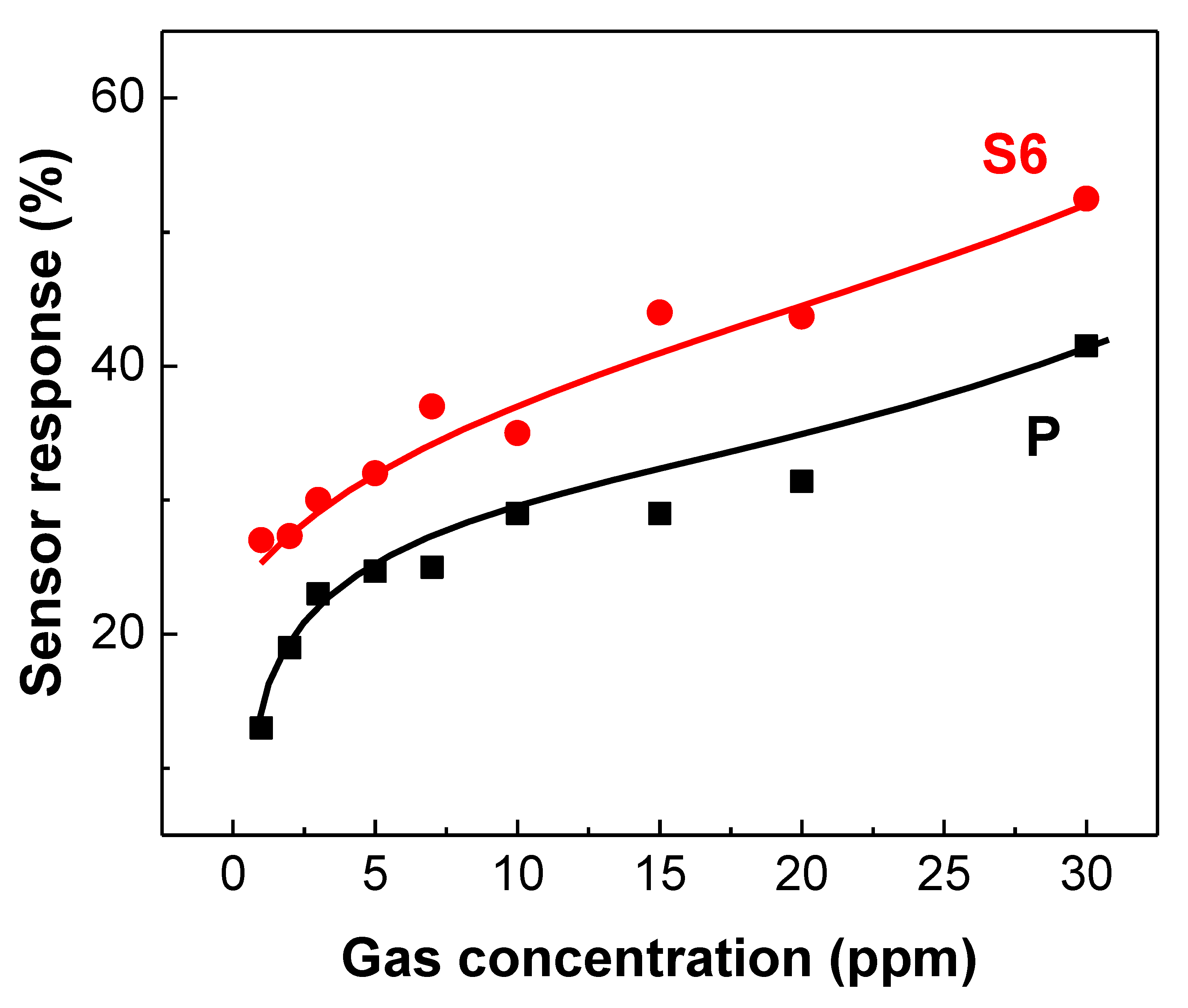
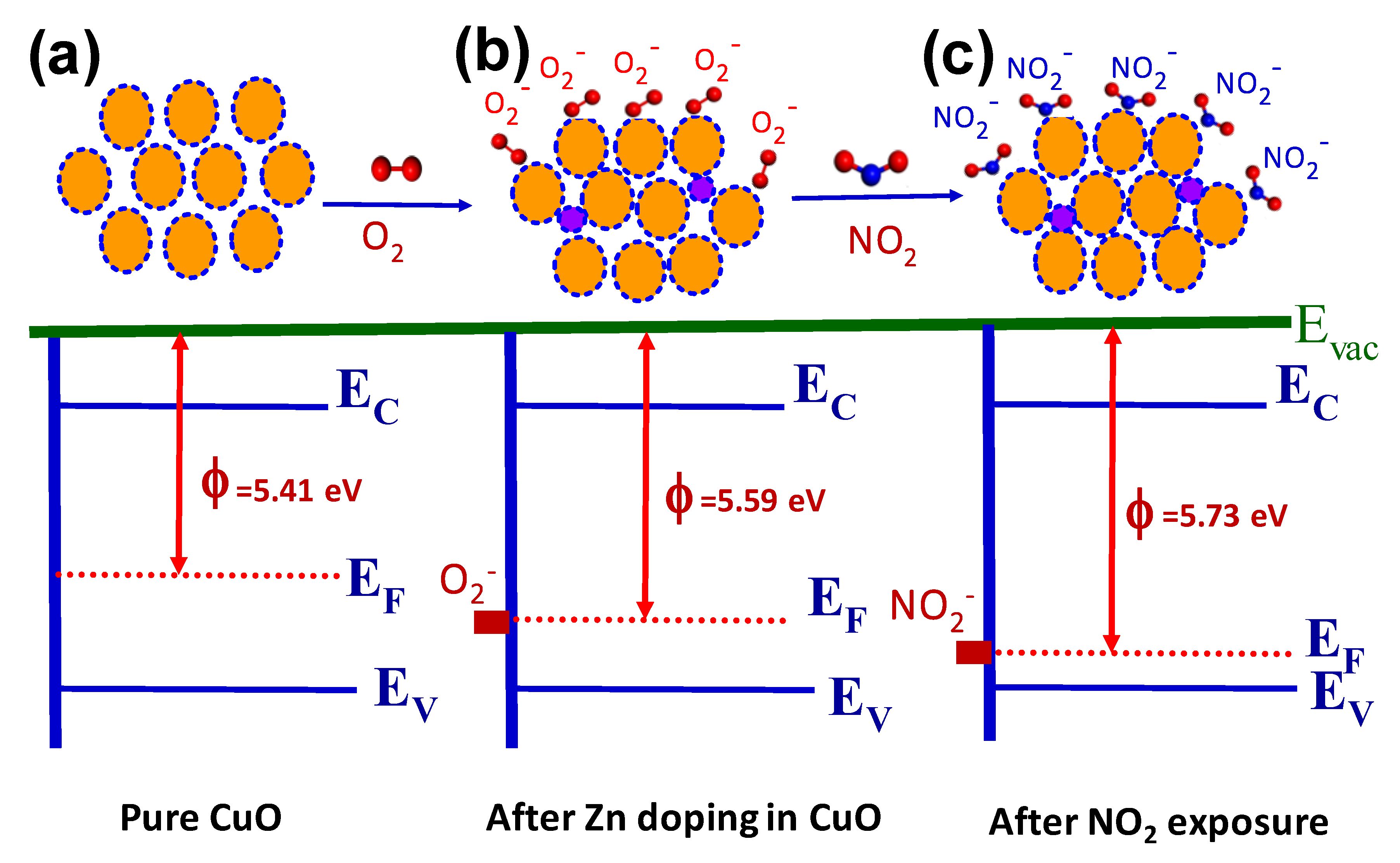
3.3. Gas Sensing Studies

Based on the previous characterizations, to know the effect of adsorbed oxygen and Zn doping, samples P and S6 were used for gas sensing investigation as other samples doped at lower concentration did not show significant changes in structural and electronic properties. All gas sensing measurements were performed at the optimum temperature of 150 °C [47,48,49,50]. Figure 10b shows the sensor response curves recorded for samples P and S6 towards 10 ppm NO2 at an operating temperature of 150 °C. Sensor films were exposed with NO2 gas for 10 sec in an airtight gas chamber, and the chamber was opened for recovery, as shown by the arrows in Figure 10, as gas in and gas out, respectively. The response time and recovery times were found to be ~10 s and ~20 mins, towards 10 ppm of NO2 for the S6 sample. The base resistance of sensor film was found to decrease after Zn doping. This was due to the enhancement of adsorbed oxygen species on the sample surface resulting in more charge carriers, lowering the film resistance compared to pristine CuO film. The variations in sensor response as a function of NO2 concentration were performed as shown in Figure 11. The sensor response for the Zn-doped sample was enhanced when compared to the pure sample. Both pure and Zn-doped CuO sensor films exhibited a linear response towards NO2 up to 30 ppm. Sensor films responded to NO2 at a low concentration of 1 ppm also. The resistance of samples P and S6 were found to be 93 and 38 kΩ before gas exposure and 81 and 28 kΩ after 1 ppm NO2 exposure at 150 °C, respectively. The stability of the sensor film is an important criterion; accordingly, the base resistance of both sensor films was measured as a function time. The base resistance of sensor films at an operating temperature of 150 °C was measured over a period of 10 days as shown in Figure 12. The base resistances of the sensor films were found to be nearly constant which confirms its stability. To check the selectivity, sensor film was exposed to the different gases, namely, NH3 (50 ppm), H2S (20 ppm), CO (300 ppm), and C2H5OH (300 ppm). A selectivity histogram is shown in Figure 13. No response was observed for these gases, even at higher concentrations, which confirms the high selectivity of the sensor film towards NO2.
To investigate the effect of doping and gas interaction towards work function (ϕ), Kelvin probe measurements were performed. Figure 14a shows the work function area map recorded for samples P and S6. The average work function values for samples P and S6 were recorded and found to be 5410 meV and 5590 meV, respectively. There was an increase in work function after Zn doping of 180 meV. This was due to the shift in Fermi levels towards the valance band after doping. The increase in charge carriers (holes) by the enhancement of adsorbed oxygen species contributed to the shifting of the Fermi level. After exposure of NO2 gas on sample S6, the work function was further increased from 5590 meV to 5720 meV as shown in Figure 14b. This was due to the shift of the Fermi level towards the valence band, as NO2 is an oxidizing gas. Similarly, a decrease in the film resistances were observed after doping and NO2 exposure which confirms our results. Similar studies were performed in our previous report [26].
Figure 15 depicts the underlying gas sensing mechanism. An energy band diagram of semiconductor material is shown with different energy levels, vacuum level (Evac), conduction band (EC), valance band (EV), and Fermi level (EF). The CuO is a p-type semiconductor material, having holes as the majority of charge carriers. The Fermi level for this p-type material as nearer to valance band as shown in Figure 15a. After Zn doping, the adsorption of oxygen species on the sample surface increased as observed in the EDS and XPS studies. This was due to the excess electrons which are provided by Zn metal (Zn2+) to the surface oxygen atoms. This influences the adsorption of the oxygen species (O2) on the sample surface. It enhances the number of charge carriers (holes) in the sensor film, so the Fermi level shifts down towards the valance band as shown in Figure 15b. This results in a further increase of the work function and, hence, film base resistance decreases after doping. Nitrogen dioxide is an oxidizing gas, when it is exposed to sensor film, provides holes. When NO2 gas is exposed to Zn-doped CuO (p-type) sensor films, the adsorbed O2 are replaced with NO2 and more holes are generated in the sensor film. Therefore, the Fermi level shifts down further towards valence band (Figure 15c), resulting in an increased work function and decreased base resistance of the sensor film. Similar results were observed in our work function studies.

4. Conclusions

Monodispersed, uniform CuO octahedral crystals were successfully fabricated using a water bath co-precipitation technique at low temperature. The effect of Zn doping towards structural, optoelectronic, and NO2 sensing properties were investigated in detail. The Zn doping resulted in the decrease in the crystallite sizes with identical d-spacing, also confirmed using XRD and TEM studies. Gas sensing studies revealed that the Zn-doped sensor exhibited a highly sensitive and selective response towards NO2 at 150 °C with a minimum detection limit of 1 ppm. Work function measurements further supported the sensing results.

Author Contributions

Conceptualization, C.P.G. and S.P.; Methodology and Experimental, C.P.G., D.G. and S.K.R.; Characterizations, C.P.G., Y.S., N.S.R. and M.N., Writing—Original Draft Preparation, C.P.G. and D.G.; Writing—Review and Editing, S.P., N.S.R. and Y.H.; Visualization, C.M. and H.I.; Supervision, S.P., H.I. and C.M. All authors have read and agreed to the published version of the manuscript.

Funding

This work is financially supported by department of physics and technology, SRMIST, Kattankulathur, Tamil Nadu, India. This research received no external funding.

Acknowledgments

We are grateful to SRMIST for providing research facilities and infrastructure. The authors thank S. Yuvraj and C. David for helping with work function measurement studies. The authors also acknowledge the Center for Instrumental Analysis, Shizuoka University, for providing characterization facilities.

Conflicts of Interest

The authors declare no conflict of interest. We did not have known competing financial interests or personal relationships that could have appeared to influence the work reported in this paper.

References

  1. Burdett, J.K.; Sevov, S. Stability of the Oxidation States of Copper. J. Am. Chem. Soc. 1995, 117, 12788–12792. [Google Scholar] [CrossRef]
  2. Scuderi, V.; Amiard, G.; Boninelli, S.; Scalese, S.; Miritello, M.; Sberna, P.M.; Impellizzeri, G.; Privitera, V. Photocatalytic activity of CuO and Cu2O nanowires. Mater. Sci. Semicond. Process. 2016, 42, 89–93. [Google Scholar] [CrossRef]
  3. Murali, D.S.; Kumar, S.; Choudhary, R.J.; Wadikar, A.D.; Jain, M.K.; Subrahmanyam, A. Synthesis of Cu2O from CuO thin films: Optical and electrical properties. AIP Adv. 2015, 5, 047143. [Google Scholar] [CrossRef]
  4. Wong, T.K.S.; Zhuk, S.; Masudy-Panah, S.; Dalapati, G.K. Current status and future prospects of copper oxide heterojunction solar cells. Materials 2016, 9, 271. [Google Scholar] [CrossRef] [PubMed]
  5. Grigore, M.; Biscu, E.; Holban, A.; Gestal, M.; Grumezescu, A. Methods of Synthesis, Properties and Biomedical Applications of CuO Nanoparticles. Pharmaceuticals 2016, 9, 75. [Google Scholar] [CrossRef] [PubMed]
  6. Ramgir, N.S.; Ganapathi, S.K.; Kaur, M.; Datta, N.; Muthe, K.P.; Aswal, D.K.; Gupta, S.K.; Yakhmi, J.V. Sub-ppm H2S sensing at room temperature using CuO thin films. Sens. Actuators B Chem. 2010, 151, 90–96. [Google Scholar] [CrossRef]
  7. Yang, C.; Su, X.; Xiao, F.; Jian, J.; Wnag, J. Gas sensing properties of CuO nanorods synthesized by a microwave-assisted hydrothermal method. Sens. Actuators B Chem. 2011, 158, 299–303. [Google Scholar] [CrossRef]
  8. Wang, F.; Li, H.; Yuan, Z.; Sun, Y.; Chang, F.; Deng, H.; Xiea, L.; Lic, H. A highly sensitive gas sensor based on CuO nanoparticles synthetized via a sol–gel method. RSC Adv. 2016, 6, 79343–79349. [Google Scholar] [CrossRef]
  9. Jayathilaka, C.; Kapaklis, V.; Siripala, W.; Jayanetti, S. Improved efficiency of electrodeposited p-CuO/n-Cu2O heterojunction solar cell. Appl. Phys. Express 2015, 8, 065503. [Google Scholar] [CrossRef]
  10. Xu, L.; Zheng, G.; Pei, S.; Wang, J. Investigation of optical bandgap variation and photoluminescence behavior in nanocrystalline CuO thin films. Optik (Stuttg) 2018, 158, 382–390. [Google Scholar] [CrossRef]
  11. Tran, T.H.; Nguyen, V.T. Copper Oxide Nanomaterials Prepared by Solution Methods, Some Properties, and Potential Applications: A Brief Review. Int. Sch. Res. Not. 2014, 2014, 1–14. [Google Scholar] [CrossRef] [PubMed]
  12. Gu, Y.; Xuan, Y.; Zhang, H.; Deng, X.; Bai, M.; Wang, L. A facile coordination precipitation route to prepare porous CuO microspheres with excellent photo-Fenton catalytic activity and electrochemical performance. Cryst. Eng. Commun. 2019, 21, 648–655. [Google Scholar] [CrossRef]
  13. Nesa, M.; Momin, M.A.; Sharmin, M.; Bhuiyan, A.H. Structural, optical and electronic properties of CuO and Zn-doped CuO: DFT based First-principles calculations. Chem. Phys. 2020, 528, 110536. [Google Scholar] [CrossRef]
  14. Jiang, T.; Wang, Y.; Meng, D.; Wang, D. One-step hydrothermal synthesis and enhanced photocatalytic performance of pine-needle-like Zn-doped CuO nanostructures. J. Mater. Sci. Mater. Electron. 2016, 27, 12884–12890. [Google Scholar] [CrossRef]
  15. Lu, J.; Wang, J.; Zou, Q.; Zhao, Y.; Fang, J.; He, S.; He, D.; Luo, Y. Catalytic performance of transition metals (Co, Ni, Zn, Mo) doped CuO-Ce0.8Zr0.2O2 based catalysts for CO preferential oxidation in H2-rich streams. J. Alloys Compd. 2019, 784, 1248–1260. [Google Scholar] [CrossRef]
  16. Guo, X.; Qiu, Z.; Mao, J.; Zhou, R. Doping effect of transition metals (Zr, Mn, Ti and Ni) on well-shaped CuO/CeO2 (rods): Nano/micro structure and catalytic performance for selective oxidation of CO in excess H2. Phys. Chem. Chem. Phys. 2018, 20, 25983–25994. [Google Scholar] [CrossRef]
  17. Zhu, Y.; Liu, X.; Jin, S.; Chen, H.; Lee, W.; Liu, M.; Chen, Y. Anionic defect engineering of transition metal oxides for oxygen reduction and evolution reactions. J. Mater. Chem. A 2019, 7, 5875–5897. [Google Scholar] [CrossRef]
  18. Sonia, S.; Jose Annsi, I.; Suresh Kumar, P.; Mangalaraj, D.; Viswanathan, C.; Ponpandian, N. Hydrothermal synthesis of novel Zn-doped CuO nanoflowers as an efficient photodegradation material for textile dyes. Mater. Lett. 2015, 144, 127–130. [Google Scholar] [CrossRef]
  19. Yathisha, R.O.; Arthoba Nayaka, Y. Structural, optical and electrical properties of zinc incorporated copper oxide nanoparticles: Doping effect of Zn. J. Mater. Sci. 2018, 53, 678–691. [Google Scholar] [CrossRef]
  20. Iqbal, J.; Jan, T.; Ul-Hassan, S.; Ahmed, I.; Mansoor, Q.; Umair Ali, M.; Abbas, F.; Ismail, M. Facile synthesis of Zn-doped CuO hierarchical nanostructures: Structural, optical and antibacterial properties. AIP Adv. 2015, 5, 127112. [Google Scholar] [CrossRef] [Green Version]
  21. Hu, J.; Zou, C.; Su, Y.; Li, M.; Han, Y.; Kong, E.S.W.; Yang, Z.; Zhang, Y. An ultrasensitive NO2 gas sensor based on a hierarchical Cu2O/CuO mesocrystal nanoflower. J. Mater. Chem. A 2018, 6, 17120–17131. [Google Scholar] [CrossRef]
  22. Wang, Y.; Liu, D.; Yin, J.; Shang, Y.; Du, J.; Kang, Z.; Wang, R.; Chen, Y.; Sun, D.; Jiang, J. An ultrafast responsive NO2 gas sensor based on a hydrogen-bonded organic framework material. Chem. Commun. 2020, 56, 703–706. [Google Scholar] [CrossRef] [PubMed]
  23. Li, X.; Shao, C.; Lu, D.; Lu, G.; Li, X.; Liu, Y. Octahedral-Like CuO/In2O3Mesocages with Double-Shell Architectures: Rational Preparation and Application in Hydrogen Sulfide Detection. ACS Appl. Mater. Interfaces 2017, 9, 44632–44640. [Google Scholar] [CrossRef] [PubMed]
  24. Bhangare, B.; Ramgir, N.S.; Jagtap, S.; Debnath, A.K.; Muthe, K.P.; Terashima, C.; Aswal, D.K.; Gosavi, S.W.; Fujishima, A. XPS and Kelvin probe studies of SnO2/RGO nanohybrids based NO2 sensors. Appl. Surf. Sci. 2019, 487, 918–929. [Google Scholar] [CrossRef]
  25. Ramgir, N.; Datta, R.; Avhad, K.; Bhusari, R.; Vedpathak, M.M.; Meera, M.; Katke, V.V.; Ravisankar, E.; Debnath, A.K.; Saha, T.K.; et al. A Table Top Static Gas Sensing Unit: Model Tpd-barc-ch. BARC Newslett. 2017, 14–18. [Google Scholar]
  26. Ramgir, N.S.; Goyal, C.P.; Sharma, P.K.; Goutam, U.K.; Bhattacharya, S.; Datta, N.; Kaur, M.; Debnath, A.K.; Aswal, D.K.; Gupta, S.K. Selective H2S sensing characteristics of CuO modified WO3 thin films. Sens. Actuators B Chem. 2013, 188, 525–532. [Google Scholar] [CrossRef]
  27. Chidambaram, D.; Vattikondala, G.; Marappan, G.; Sivalingam, Y. Indium content dependent VOCs interactions in monolithic InGaN/GaN multi quantum well structures grown by MOCVD. Mater. Sci. Semicond. Process. 2019, 104, 104694. [Google Scholar] [CrossRef]
  28. Samarasekara, P.; Karunarathna, P.G.D.C.K.; Weeramuni, H.P.; Fernando, C.A.N. Electrical properties of spin coated Zn-doped CuO films. Mater. Res. Express 2018, 5, 066418. [Google Scholar] [CrossRef]
  29. Cretu, V.; Postica, V.; Mishra, A.K.; Hoppe, M.; Tiginyanu, I.; Mishra, Y.K.; Chow, L.; De Leeuw, N.H.; Adelung, R.; Lupan, O. Synthesis, characterization and DFT studies of zinc-doped copper oxide nanocrystals for gas sensing applications. J. Mater. Chem. A 2016, 4, 6527–6539. [Google Scholar] [CrossRef] [Green Version]
  30. Nath, D.; Singh, F.; Das, R. X-ray diffraction analysis by Williamson-Hall, Halder-Wagner and size-strain plot methods of CdSe nanoparticles- a comparative study. Mater. Chem. Phys. 2020, 239, 122021. [Google Scholar] [CrossRef]
  31. Xu, J.; Ji, W.; Shen, Z.; Li, W.; Tang, S.; Ye, X.; Jia, D.; Xin, X. Raman spectra of CuO nanocrystals. J. Raman Spectrosc. 1999, 30, 413–415. [Google Scholar] [CrossRef]
  32. Sriyutha Murthy, P.; Venugopalan, V.P.; Arunya, D.D.; Dhara, S.; Pandiyan, R.; Tyagi, A.K. Antibiofilm activity of nano sized CuO. In Proceedings of the International Conference on Nanoscience, Engineering and Technology, ICONSET 2011, Chennai, Tamilnadu, 28–30 November 2011; pp. 580–583. [Google Scholar]
  33. Jan, T.; Iqbal, J.; Farooq, U.; Gul, A.; Abbasi, R.; Ahmad, I.; Malik, M. Structural, Raman and optical characteristics of Sn doped CuO nanostructures: A novel anticancer agent. Ceram. Int. 2015, 41, 13074–13079. [Google Scholar] [CrossRef]
  34. Zheng, X.; Chen, W.; Wang, G.; Yu, Y.; Qin, S.; Fang, J.; Wang, F.; Zhang, X.A. The Raman redshift of graphene impacted by gold nanoparticles. AIP Adv. 2015, 5, 057133. [Google Scholar] [CrossRef]
  35. Jacquemin, M.; Genet, M.J.; Gaigneaux, E.M.; Debecker, D.P. Calibration of the X-ray photoelectron spectroscopy binding energy scale for the characterization of heterogeneous catalysts: Is everything really under control? ChemPhysChem 2013, 14, 3618–3626. [Google Scholar] [CrossRef] [PubMed]
  36. Xu, J.F.; Ji, W.; Shen, Z.X.; Tang, S.H.; Ye, X.R.; Jia, D.Z.; Xin, X.Q. Preparation and Characterization of CuO Nanocrystals. J. Solid State Chem. 1999, 147, 516–519. [Google Scholar] [CrossRef]
  37. Li, K.; Xue, D. Estimation of Electronegativity Values of Elements in Different Valence States. J. Phys. Chem. A 2006, 110, 11332–11337. [Google Scholar] [CrossRef]
  38. Qiu, X.; Burda, C. Chemically synthesized nitrogen-doped metal oxide nanoparticles. Chem. Phys. 2007, 339, 1–10. [Google Scholar] [CrossRef]
  39. Zhu, L.; Li, H.; Liu, Z.; Xia, P.; Xie, Y.; Xiong, D. Synthesis of the 0D/3D CuO/ZnO Heterojunction with Enhanced Photocatalytic Activity. J. Phys. Chem. C 2018, 122, 9531–9539. [Google Scholar] [CrossRef]
  40. Dupin, J.C.; Gonbeau, D.; Vinatier, P.; Levasseur, A. Systematic XPS studies of metal oxides, hydroxides and peroxides. Phys. Chem. Chem. Phys. 2000, 2, 1319–1324. [Google Scholar] [CrossRef]
  41. Ciftyürek, E.; Šmíd, B.; Li, Z.; Matolín, V.; Schierbaum, K. Spectroscopic understanding of Sno2 and Wo3 metal oxide surfaces with advanced synchrotron based; XPS-UPS and near ambient pressure (NAP) XPS surface sensitive techniques for gas sensor applications under operational conditions. Sensors 2019, 19, 4737. [Google Scholar] [CrossRef] [Green Version]
  42. Kowalczyk, S.P.; Ley, L.; McFeely, F.R.; Pollak, R.A.; Shirley, D.A. Relative effect of extra-atomic relaxation on Auger and binding-energy shifts in transition metals and salts. Phys. Rev. B 1974, 9, 381–391. [Google Scholar] [CrossRef]
  43. Alexander, V.N.; Anna, K.V.; Stephen, W.G.; Powell, C.J. NIST X-ray Photoelectron Spectroscopy Database. Available online: http://srdata.nist.gov/xps/Default.aspx (accessed on 14 February 2020).
  44. Bhuvaneshwari, S.; Gopalakrishnan, N. Hydrothermally synthesized Copper Oxide (CuO) superstructures for ammonia sensing. J. Colloid Interface Sci. 2016, 480, 76–84. [Google Scholar] [CrossRef] [PubMed]
  45. Manoharan, C.; Pavithra, G.; Bououdina, M.; Dhanapandian, S.; Dhamodharan, P. Characterization and study of antibacterial activity of spray pyrolysed ZnO:Al thin films. Appl. Nanosci. 2016, 6, 815–825. [Google Scholar] [CrossRef] [Green Version]
  46. Vuong, N.M.; Chinh, N.D.; Huy, B.T.; Lee, Y.I. CuO-decorated ZnO hierarchical nanostructures as efficient and established sensing materials for H2S Gas Sensors. Sci. Rep. 2016, 6, 1–13. [Google Scholar] [CrossRef] [PubMed] [Green Version]
  47. Chowdhuri, A.; Gupta, V.; Sreenivas, K. Enhanced catalytic activity of ultrathin CuO islands on SnO2 films for fast response H2S gas sensors. IEEE Sens. J. 2003, 3, 680–686. [Google Scholar] [CrossRef]
  48. Navazani, S.; Shokuhfar, A.; Hassanisadi, M.; Di Carlo, A.; Yaghoobi Nia, N.; Agresti, A. A PdPt decorated SnO2-rGO nanohybrid for high-performance resistive sensing of methane. J. Taiwan Inst. Chem. Eng. 2019, 95, 438–451. [Google Scholar] [CrossRef]
  49. Kooti, M.; Keshtkar, S.; Askarieh, M.; Rashidi, A. Progress toward a novel methane gas sensor based on SnO2 nanorods-nanoporous graphene hybrid. Sens. Actuators B Chem. 2019, 281, 96–106. [Google Scholar] [CrossRef]
  50. Jaaniso, R.; Tan, O.K. Semiconductor Gas Sensors; Elsevier: Amsterdam, The Netherlands, 2013; ISBN 9780857092366. [Google Scholar]
Figure 1. X-ray diffraction patterns of pure and Zn-doped CuO films.
Crystals 10 00188 g001
Figure 2. (a) XRD peak ( 1 ¯ 1 1) of pure and Zn-doped CuO films and (b) the change in the crystallite size and strain as a function of Zn concentration.
Crystals 10 00188 g002
Figure 3. Raman spectra of pure and Zn-doped CuO films.
Crystals 10 00188 g003
Figure 4. FESEM images of pure and Zn-doped CuO films for (a) P, (b) S3, and (c) S6.
Crystals 10 00188 g004
Figure 5. (a) Elemental mapping and (b) EDS spectra of sample S6.
Crystals 10 00188 g005
Figure 6. TEM images of pure and Zn-doped CuO samples (a) P, (b) S3, and (c) S6.
Crystals 10 00188 g006
Figure 7. STEM image with elemental mapping of sample S6.
Crystals 10 00188 g007
Figure 8. X-ray photoelectron spectra of (a) Cu 2p, (b) O 1s, and (c) Zn 2p for pure and Zn-doped CuO films.
Crystals 10 00188 g008
Figure 9. Photoluminescence (PL) spectra of pure and Zn-doped CuO films.
Crystals 10 00188 g009
Figure 10. (a) Schematic of fabricated gas sensor device and the (b) response curves recorded for pure and Zn-doped CuO films towards 10 ppm of NO2 at an operating temperature of 150 °C.
Crystals 10 00188 g010
Figure 11. Variation in sensor response (%) as a function of NO2 concentration recorded for both pure and Zn-doped CuO films at 150 °C.
Crystals 10 00188 g011
Figure 12. Long-term stability measurements of base resistance for pure and Zn-doped CuO films at an operating temperature of 150 °C.
Crystals 10 00188 g012
Figure 13. Selectivity histogram for sample S6 at an operating temperature of 150 °C.
Crystals 10 00188 g013
Figure 14. Work function area map (2 mm × 2 mm) recorded for both (a) samples P and S6 and (b) the change in the work function of sample S6 upon exposure to 50 ppm NO2.
Crystals 10 00188 g014
Figure 15. Schematic representation of the NO2 sensing mechanism; work function of (a) pure CuO, and changes after (b) Zn doping and (c) NO2 exposure.
Crystals 10 00188 g015
Table 1. Elemental composition of pure and Zn-doped CuO films.
SampleComposition (atomic %)
CuOZn
P68.6431.36-
S166.6832.430.89
S264.2134.441.35
S368.1030.171.73
S468.0629.951.99
S565.1731.733.10
S652.1241.196.69

