Article

Three-Dimensional CA-LBM Model of Silicon Facet Formation during Directional Solidification

School of Materials Science and Engineering, Hebei University of Technology, Tianjin 300132, China
*
Authors to whom correspondence should be addressed.
Crystals 2020, 10(8), 669; https://doi.org/10.3390/cryst10080669
Submission received: 2 July 2020 / Revised: 25 July 2020 / Accepted: 27 July 2020 / Published: 3 August 2020

Abstract

:
A new 3D cellular automata-lattice Boltzmann method (CA-LBM) coupling model is proposed to simulate the formation of facet and facet dendrites in directional solidification. In this model, the CA method is used to simulate the crystal growth process and the LBM method is used to simulate the physical field in the calculation area. A new three-dimensional anisotropic function is introduced, and the model is modified by interpolation and neighborhood restriction. We add the remelting calculation model. The interaction between interface energy anisotropy and dynamic anisotropy is solved reasonably. The growth process and morphology of small plane and small plane dendrites were simulated.

1. Introduction

At present, the polycrystalline silicon produced by directional solidification is still the main material of photoelectric conversion for solar cells. It is of great significance to improve the quality of polysilicon and the production efficiency of polysilicon by using numerical simulation to guide the formulation of the main process parameters of polysilicon directional solidification.
Since 2001, scholars have used numerical methods to calculate the temperature field and flow field of directional solidification of polysilicon, effectively guiding the actual production of polysilicon [1,2,3,4,5]. In recent years, the numerical simulation of polycrystalline silicon has gradually moved from the calculation of macroscopical field to the coupling calculation of the growth process of the microstructure, in order to obtain more real solidification information and control the solidification process of polycrystalline silicon more accurately.
So far, the numerical methods used to simulate crystal growth mainly focus on phase field method and cellular automaton. In addition, because the Jacson factor of Si is greater than 2.0 [6], the growth interface shows significant facet characteristics, so the phase field (PF) method used to calculate the growth of silicon crystal is different from the PF method of non-facet crystal represented by metal. In recent years, the PF method was first used to study the growth characteristics of silicon crystals, such as Lin et al. [7,8,9,10]. The characteristic of the PF method is that the liquid/solid interface is a continuous transition interface, which is more effective for accurately depicting the characteristics of growth interface. However, the thickness of transition interface limits the grid scale of PF method, greatly increases the calculation amount, reduces the calculation scale and efficiency. For the directional solidification process of polysilicon for industrial use, it is not necessary to control the process parameters accurately to the level of 10−3 μm at present. It can obtain the micro characteristics of facet (1–100 μm). In this case, the CA method is more appropriate.
In recent years, firstly, the columnar equiaxed transformation (CET) process of silicon crystal directional solidification was simulated by the CA-LBM method by Lian et al. [11], then Zhang et al. [12] calculated the facet characteristics of silicon by the CA method for the first time, and calculated the growth process of single silicon equiaxed crystal and the CET process of silicon directional solidification by the coupling LBM method. Wang et al. [12]. Further improved and perfected the facet crystal growth model of silicon, making the facet characteristics more accurate.
However, Lian, Zhang and Wang’s models are all two-dimensional models, which cannot fully reflect the growth process of silicon facet crystal. Based on the research of Lian et al., this paper intends to expand the two-dimensional model to the three-dimensional model, in order to obtain a more real formation process of the silicon facet microstructure.

2. Materials and Methods

Under the conditions of small Peclet number [13] and low Reynolds number [13], a three-dimensional CA-LBM coupling model with high interface energy anisotropy and dynamic anisotropy is established. The temperature field is calculated by LB method, the solid-liquid interface advancing process is calculated by CA method, and the CA method and LBM method are coupled according to the solidification latent heat released by the solid-state rate growth of silicon crystal. The experimental results are compared with the simulation results to verify the correctness and availability of the model.

2.1. LBM Model

Single relaxation time Latice Bhatnagar-Gross-Krook (LBGK) method, D3Q15 model [13].
f i ( r + e i Δ t , t + Δ t ) = f i ( r , t ) + 1 τ f ( f i e q ( r , t ) f i ( r , t ) ) + F i
F i = ( 1 1 2 τ f ) w i ( 3 e i u c 2 + 9 e i u c 4 ) Δ t F
where r and t represent location and time respectively. Δt represents the time step. ei is the speed in i direction. τf is the relaxation time of temperature. The relaxation time represents the time when the distribution function (fi) of each particle approaches its equilibrium distribution function (fieq). fi is the distribution function of particle temperature, and fieq is the equilibrium distribution function of particle temperature. Fi is the heat source term, which is the latent heat released during the growth of silicon. F is liquid buoyancy.

2.2. CA Model

In this paper, the three-dimensional CA model is used to simulate the growth of a silicon facet, whereby 150 × 150 × 150 cells are selected in the calculation area, and the cell size is 1 μm.
The following is a three-dimensional model to simulate the growth and capture of silicon facet.

2.2.1. Model for the Growth

The supercooling at the front of crystal melt interface includes thermodynamic supercooling and curvature supercooling.
Δ T = T L T + Γ K a s ( n )
where TL is the liquidus temperature, T represents the node temperature of grid cell, Г is the Gibbs Thomson coefficient, K is the curvature of the interface, and K is calculated from Equation (4) [14].
K = 1 Δ x [ 1 2 ( f s + i = 1 N f s i ) / ( N + 1 ) ]
where Δx is the cell size, fsi is the solid fraction of the nearest cell, and N is the total number of adjacent cells in the first level. In this paper, the total number of cells in the first layer of three-dimensional CA model is 26.

2.2.2. Remelting Calculation

If the module is not added, the solid-state ratio of silicon can only be accumulated on the cube cell with sharp and sharp solid-state ratio of 1, and the interface cell can be captured on this basis.
Melting means that when the supercooling of cell is not negative, the growth rate is not negative, and then the change value of solid phase rate is negative, that is, the solid phase melts. When the solid phase rate of the interface cell decreases to 0, the cell is transformed into liquid phase cell, at the same time, the adjacent solid phase cell is captured and transformed into interface cell. Then, the solid phase is melted.
After adding the remelting procedure, the cubic cell with solid ratio of 1 will melt gradually and form interface cell because of the large curvature supercooling at the corner and the low thermodynamics supercooling at the initial stage of solidification. On this basis, the next generation and capture will be carried out, and the calculation results are more reasonable.
In order to keep the solid–liquid interface of the single layer as well as the solidification and growth, the geometric parameter g, which is related to the state of adjacent grid, is introduced.
g = min ( ( m = 1 6 S m χ 1 + 1 2 m = 1 12 S m χ 2 ) / 2.1 )
For solidification interface:
S χ 1 , S χ 2 = { 0 , ( f s < 1 ) 1 , ( f s = 1 )
For melting interface:
S χ 1 , S χ 2 = { 0 , ( f s > 0 ) 1 , ( f s = 0 )
where S χ 1 is the state parameter of the nearest six grids. S χ 2 is the state parameter of the next nearest 12 grids. When the growth rate νe > 0, it solidifies. Otherwise, it melts.
In order to get a more accurate value of the interface curvature, bilinear interpolation method [1] is used to calculate the interpolation in space, so as to reduce the anisotropy of the cube grid.
As shown in Figure 1, the red ball is the node that divides the cube grid, the white ball is the inserted value, marked as Pi (i = 1~8), and its position is the center of the cube composed of eight red balls around. The average value of each Pi is obtained from the solid phase ratio values of eight nodes around it (the red ball position).
as(n) is is a highly anisotropic interface energy function, which is obtained from Equation (8).
a s ( n ) = ( n x k + n y k + n z k ) α / k
where nx, ny and nz are the normal directions of the interface in x−, y−, and z− directions respectively. α and k are parameters that affect the strength of anisotropy.
The relationship between growth rate and undercooling is in the form of Fujiwara [15,16], see Formula (9)
v e = μ ( n ) Δ T g
where, νe is the growth rate formula, μ(n) is the growth rate coefficient, see Equation (10)
μ ( n ) = μ ¯ ( a s 2 ( n ) + W 0 a s ( n ) t s ( n ) ) 1
where μ ¯ is the angular mean of the dynamic coefficients, as(n) represents the anisotropic function of interface free energy, W0 represents parameters related to average diffusivity and kinetics, ts(n) is a dynamic anisotropic function. The dynamic anisotropic function ts(n) is set to as(n)−4.

2.2.3. Model for the Capture

The computational grid is made up of cube cells. The states of each cell are divided into three different states according to its solid fraction fs(t). When fs(t) is 0, it means that the cell is a liquid cell. When fs(t) is 1, it means that the cell is a solid cell. When 0 < fs(t) < 1, it means that the cell is an interface cell, that is, a solid-liquid mixed cell.
When the solid fraction of the interface cell accumulates and becomes solid, the cell captures the liquid cell adjacent to its space, and the adjacent liquid cell is captured and transformed into the interface cell and enters the growth state.
For the three-dimensional CA model, each cell has 6 nearest neighbor cells in the direction of <100>. The next nearest neighbor cells in 12 <110> directions and 8 <111> directions. Therefore, 3D capture rules are much more complex than 2D capture rules. At present, it is difficult to get the method of capturing the grid with low anisotropy, so this paper chooses the simplest six neighbor acquisition method, and uses the three-dimensional neighborhood restriction method [17] to reduce the anisotropy of the grid itself.
The three-dimensional limit neighborhood solid fraction method (LNSF): (1) The average solid fraction f ¯ s of liquid cell was calculated. (2) Set the limit neighborhood capture fraction fsLNSF. If f ¯ s f s L N S F , and has the conditions to be captured, the cell is captured.
In this paper, the capture method of 3D CA model is a combination of von Neumann method and 3D neighborhood restriction method, The von Neumann method ensures that the model is a sharp interface, and LNSF greatly reduces the anisotropy of the cube grid itself.
The calculation equation of growth rate is given by Equation (10), and the length of crystal growth is given by Equation (11):
l ( t ) = t t + δ t v e ( Δ T ( t ) ) d t cos θ + sin θ
where δt is the calculation time step, θ is the optimal angle, and 0 is taken. The solid fraction fs(t) can be obtained from Equation (12).
f s ( t ) = l ( t ) δ x
where δx is the distance between two adjacent cells. When the solid fraction fs(t) ≥ 1, that is to say, the growth front of the growth cell has contacted the center line of the adjacent liquid cell, the growth cell is transformed into the solid cell, and the liquid cell into the growth cell.

2.3. The Physical Parameters of Silicon Melt

The physical properties used in the present computations are listed in Table 1 [18,19].

3. Results and Discussion

3.1. Anisotropy of Interfacial Free Energy

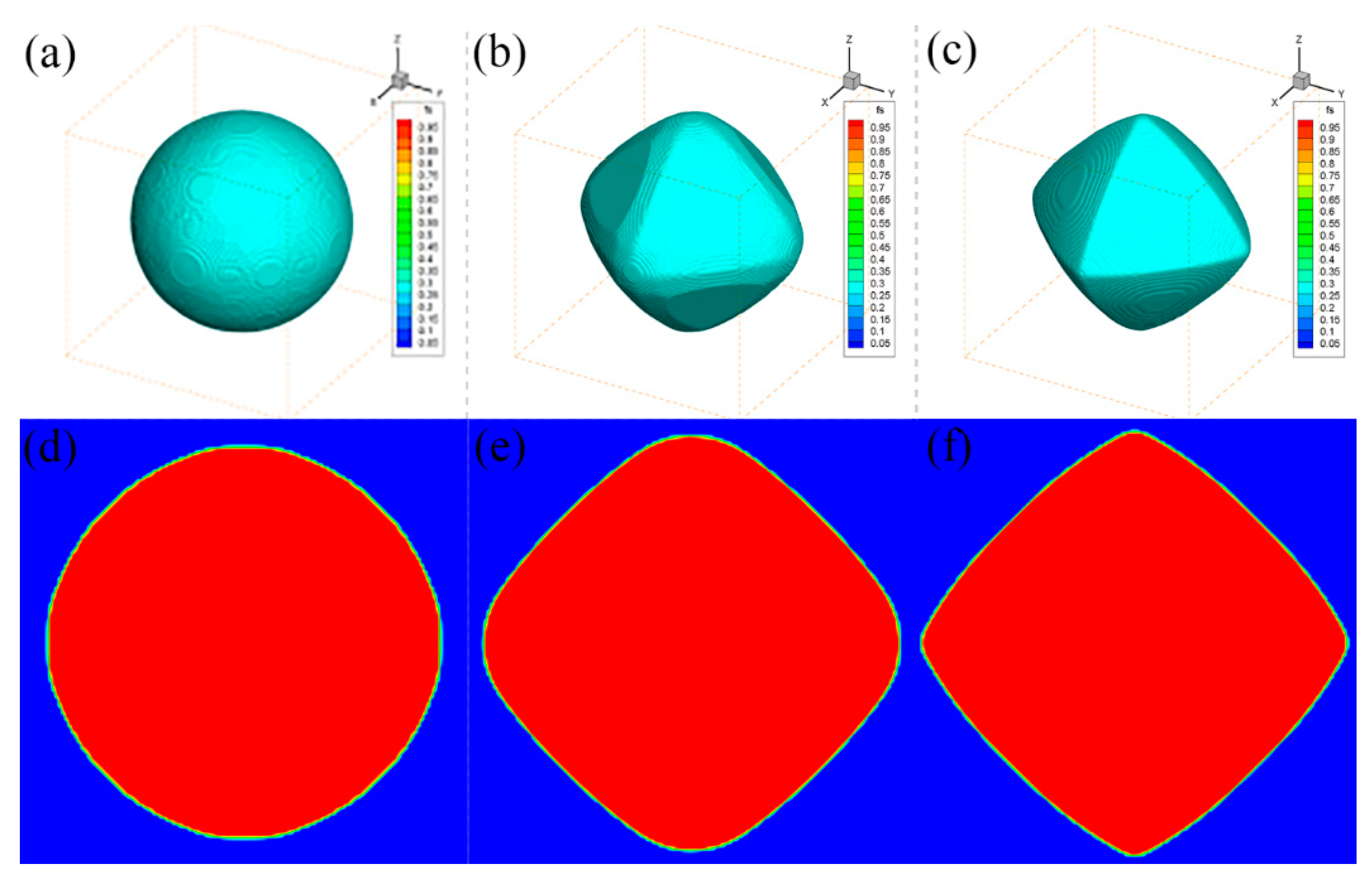
In order to study the effect of three-dimensional interfacial free energy anisotropy on the growth of silicon crystal, the values of interfacial energy anisotropy with different strength were calculated. As shown in Figure 2a–c are the calculation results when the anisotropic parameters of interface energy are α = 1.5, k = 2, 5.5 and 9.5, respectively. The upper part of each drawing is the 3D simulation result display, and the lower part is the middle section corresponding to the 3D drawing.
It can be seen from Figure 2a that when the anisotropy parameter of the interface energy is k = 2, the anisotropy is very small. The growth result from the spherical core is still spherical. The anisotropy parameter of Figure 2b is k = 5.5. It can be seen from the three-dimensional and cross-section figures that the growth result is more anisotropic than that of Figure 2a, but the top corner is still round. Figure 2c shows the anisotropic parameter k = 9.5, and it can be seen from the figure that there is a large anisotropic feature. The final simulation results show a sharp top angle and a flat surface. This is due to the different anisotropy in different directions, which affects the growth rate of silicon crystal. Finally, the typical anisotropic morphology is formed.
The simulation in Figure 3 is initially spherical core, and the anisotropic strength is taken as 1.5/9.5, and the dynamic anisotropy is as(n)−4 [9].
Figure 3a shows the results of the three-dimensional solid ratio of the equilibrium shape of the numerical simulation. It can be seen that the three-dimensional results are the standard octahedral shape, showing a typical effect of high anisotropy.
Figure 3b is a cross-section of the solid ratio results in Figure 3a and a comparison between the simulation and the analytical solution. It can be seen from the figure that the coincidence is high, and the analytical solution is from Wang et al. [20].
Figure 3c output result profile of solid-liquid interface at equal time intervals. The output time interval is 1000 calculation time steps. From the figure, we can clearly see the evolution process of solid-liquid interface, that is, from circular core to regular quadrilateral, showing the obvious anisotropic growth characteristics.
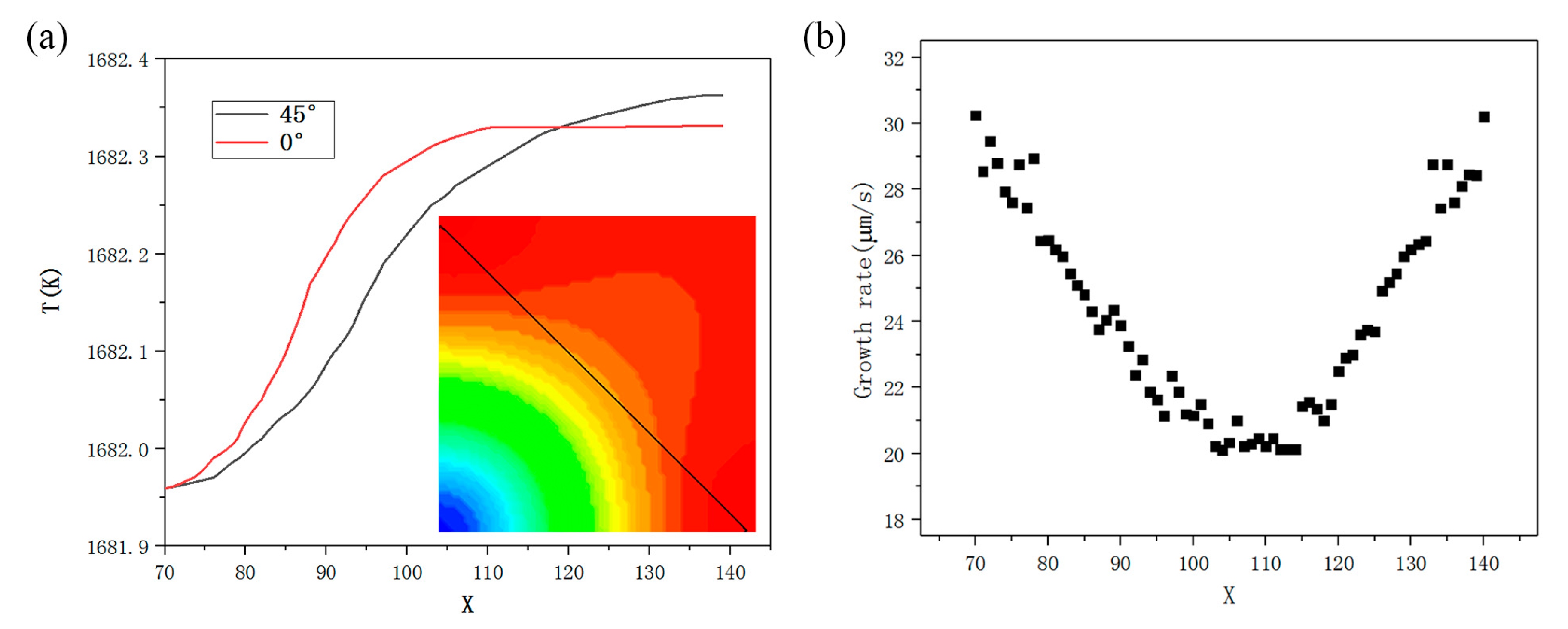
The difference of crystal growth morphology caused by the anisotropy of interface energy is also reflected in the temperature field of different growth directions. From the simulation results in Figure 4a, it can be seen that the temperature curve of (100) preferred growth direction (marked as 0° direction in the figure) rises rapidly at the beginning of growth, then the temperature curve area is gentle and finally close to the level. Compared with the temperature curve in the (111) direction, the temperature curve in the (111) direction (marked as 45° in the figure) presents a relatively gentle temperature rise, and finally crosses the temperature curve in the vertical direction, which is higher than the vertical direction. The lower right corner of Figure 4a is the quarter temperature field distribution.
As shown in Figure 4a, because the growth rate in the preferred growth direction is fast and the released latent heat of crystallization is fast, the temperature curve in this direction will increase rapidly. After a certain period of growth, the released latent heat of solidification will further accumulate, reducing the supercooling and slowing down the growth rate. During this period, the latent heat of solidification generated in the preferred growth direction will also accumulate laterally to the weak anisotropy in the direction of, the temperature increases slowly, and further inhibits the growth of the direction.
Figure 4b is the scatter diagram of the growth rate distribution of the solid-liquid interface in Figure 4a. It can be seen from the figure that the growth rate in the 0° directions is higher than that in the 45° direction due to the influence of anisotropic strength. So, when the coordinate x-coordinate increases from 70 to 140, the growth rate shows a trend from high to low and then to high. This is also the reason for the formation of facet. It can be concluded that the results of the whole simulation are in dynamic equilibrium.

3.2. Simulations for Facet Formation

Two intersecting sine waves are used as the initial shape of solid-liquid interface propulsion calculation, and the anisotropic strength value is 1.5/9.5. The dynamic anisotropy is set to as(n)−4 [9] and the simulation results are shown in Figure 5.
At the early stage of growth, the top and bottom of the initial morphology are anisotropic, so the growth speed is faster, which makes the heat generated at the top and bottom more. Because of the rapid growth speed of the top, for the top, the rapid growth speed at the initial stage will cause the growth interface to break into the supercooled liquid, which will form a negative temperature gradient, and the growth speed will increase. However, due to the solidification latent heat released by the growth and when the top gradually becomes sharp, the curvature supercooling will increase rapidly. Therefore, in the equilibrium state of temperature and curvature supercooling, the vertex angle of the facet is formed.
For the bottom, due to the low cooling rate, the heat released during its growth will gather at the bottom, and some will form small sharp corners, which will be swallowed during the growth process. In some places, there is no sharp angle, because the solidification latent heat released around the bottom gathers at the bottom, and the temperature rises, thus inhibiting its growth. As time goes on, the whole interface is stable, forming a typical facet interface.
As shown in Figure 6, it is the temperature field distribution diagram, in which the black line is the solid-liquid interface. It can be clearly seen that the heat accumulation in the facet concave corner, due to the temperature rise, thus inhibiting the growth speed of the facet concave corner to promote the formation of facet. When the tip extends into the melt with larger undercooling, the curvature of the top is smaller when the tip angle is not formed, so the temperature is the dominant factor, so the growth speed at the tip is greater than that at the bottom. When a sharp angle is formed at the top, the supercooling of curvature at the top will increase, so it will reach a stable state.
Figure 7 shows the simulation result of facet dendrite, and the boundary condition is hexahedral adiabatic. Figure 7a is a three-dimensional facet. The zigzag shape on the primary diameter arm can be seen from the figure, which is consistent with the relevant simulation [9,10]. Figure 7b shows the temperature field and solid-liquid interface morphology. Figure 7c is a quarter enlarged view of dendrite. From Figure 7b,c, it can be seen that the anisotropy of the facet dendrites is higher than that of the non-facet dendrites, and the facet and orientation missing appear at the concave angle a between the arms of the dendrites. There is a phenomenon of annexation in the process of facet growth at B, that is, there are two original facets growing and merging into a larger facet. When the six sides are adiabatic, the released latent heat of solidification diffuses into the melt, resulting in a negative temperature gradient, and the isotherm is concave.

4. Conclusions

In this paper, a new three-dimensional anisotropic function is introduced, and a three-dimensional CA model is established to simulate the formation of a silicon facet and the three-dimensional facet dendrite. The interpolation method and neighborhood restriction method are used to modify the model. The interaction between interface energy anisotropy and dynamic anisotropy is solved reasonably. The successful simulation of the self-programming CA model shows that the CA model is superior to the macro micro coupling model, which paves the way for further increasing the size of simulation calculation and the application of large-scale parallel computing in the future.

Author Contributions

Conceptualization, R.L. and H.C.; Data curation, W.M.; Formal analysis, W.M.; Investigation, W.M.; Methodology, R.L. and H.C.; Resources, H.C.; Software, W.M.; Writing – original draft, W.M.; Writing – review & editing, W.M., R.L. and H.C. All authors have read and agreed to the published version of the manuscript.

Funding

This research was funded by a grant from the National Natural Science Foundation of China (grant No. 51475138 and No. 51975182) and 2019 Tongliao Science and Technology Innovation Guidance Incentive Fund.

Acknowledgments

L.L. would like to thank Ri Li and Hongjian Chen (Hebei University of Technology) for providing academic guidance.

Conflicts of Interest

The authors declare no conflict of interest.

References

  1. Steinbach, I.; Apel, M.; Rettelbach, T.; Franke, D. Numerical simulations for silicon crystallization processes—Examples from ingot and ribbon casting. Sol. Energy Mater. Sol. Cells 2002, 72, 59–68. [Google Scholar] [CrossRef]
  2. Vizman, D.; Friedrich, J.; Müller, G. Comparison of the predictions from 3D numerical simulation with temperature distributions measured in Si Czochralski melts under the influence of different magnetic fields. J. Cryst. Growth 2001, 230, 73–80. [Google Scholar] [CrossRef]
  3. Kalaev, V.V.; Lukanin, D.P.; Zabelin, V.A.; Makarov, Y.N.; Virbulis, J.; Dornberger, E.; Von Ammon, W. Calculation of bulk defects in CZ Si growth: Impact of melt turbulent fluctuations. J. Cryst. Growth 2003, 250, 203–208. [Google Scholar] [CrossRef]
  4. Liu, L.; Kakimoto, K. Partly three-dimensional global modeling of a silicon Czochralski furnace. I. Principles, formulation and implementation of the model. Int. J. Heat Mass Transf. 2005, 48, 4481–4491. [Google Scholar] [CrossRef]
  5. Habler, C.; Stollwerck, G.; Koch, W.; Krumbe, W.; Muller, A.; Franke, D.; Rettelbach, T. Multicrystalline silicon for solar cells: Process development by numerical simulation. Adv. Mater. 2001, 13, 1815–1819. [Google Scholar]
  6. Jackson, K.A. Crystal growth kinetics. Mater. Sci. Eng. 1984, 65, 7–13. [Google Scholar] [CrossRef]
  7. Lin, H.K.; Chen, H.Y.; Lan, C.W. Phase field modeling of facet formation during directional solidification of silicon film. J. Cryst. Growth 2014, 385, 134–139. [Google Scholar] [CrossRef]
  8. Lin, H.K.; Lan, C.W. Three-dimensional phase field modeling of silicon thin-film growth during directional solidification: Facet formation and grain competition. J. Cryst. Growth 2014, 401, 740–747. [Google Scholar] [CrossRef]
  9. Chen, G.Y.; Lan, C.W. Understanding the facet formation mechanisms of Si thin-film solidification through three-dimensional phase-field modeling. J. Cryst. Growth 2016, 474, 166–170. [Google Scholar] [CrossRef]
  10. Zhi, C.; Chen, C.L.; Hao, L.M. Numerical simulation of facet dendrite growth. Trans. Nonferrous Met. Soc. China 2008, 18, 938–943. [Google Scholar]
  11. Lian, Q.; Liu, W.; Li, R.; Yan, W.; Liu, C.; Zhang, Y.; Wang, L.; Chen, H. Numerical simulation of multi-crystalline silicon crystal growth using a macro-micro coupled method during the directional solidifification process. Appl. Sci. 2016, 7, 21. [Google Scholar] [CrossRef] [Green Version]
  12. Zhang, Y.X.; Li, R.; Wang, J.; Wang, L.X.; Yan, W.B.; Liu, C.C.; Chen, H.J. Cellular automaton modeling of the transition of multi-crystalline silicon from a planar faceted front to equiaxed growth. Appl. Sci. 2017, 7, 13. [Google Scholar]
  13. Chen, R.; Xu, Q.; Liu, B. Cellular automaton simulation of three-dimensional dendrite growth in Al–7Si–Mg ternary aluminum alloys. Comput. Mater. Sci. 2015, 105, 90–100. [Google Scholar] [CrossRef] [Green Version]
  14. Nastac, L. Numerical modeling of solidification morphologies and segregation patterns in cast dendritic alloys. Acta Mater. 1999, 47, 4253–4262. [Google Scholar] [CrossRef]
  15. Fujiwara, K.; Obinata, Y.; Ujihara, T.; Usami, N.; Sazaki, G.; Nakajima, K. Grain growth behaviors of polycrystalline silicon during melt growth processes. J. Cryst. Growth. 2004, 266, 441–448. [Google Scholar] [CrossRef]
  16. Fujiwara, K.; Obinata, Y.; Ujihara, T.; Usami, N.; Sazaki, G.; Nakajima, K. In-situ observations of melt growth behavior of polycrystalline silicon. J. Cryst. Growth. 2004, 262, 124–129. [Google Scholar] [CrossRef]
  17. Lei, W.; Xin, L.; Meng, W.; Huang, W. Orientation selection of equiaxed dendritic growth by three-dimensional cellular automaton model. Physical B 2012, 407, 2471–2475. [Google Scholar]
  18. Qiu, S.; Wen, S.; Fang, M.; Zhang, L.; Gan, C.; Jiang, D.; Tan, Y.; Li, J.; Luo, X. Process parameters inflfluenceI. Vacuum 2016, 125, 40–47. [Google Scholar] [CrossRef]
  19. Desai, P.D. Thermodynamic properties of iron and silicon. J. Phys. Chem. Ref. Date 1986, 15, 967–983. [Google Scholar] [CrossRef]
  20. Burton, W.K.; Cabrera, N.; Frank, F.C. The growth of crystals and the equilibrium structure of their surfaces. Philos. Trans. R. Soc. Lond. A 1951, 243, 299–358. [Google Scholar]
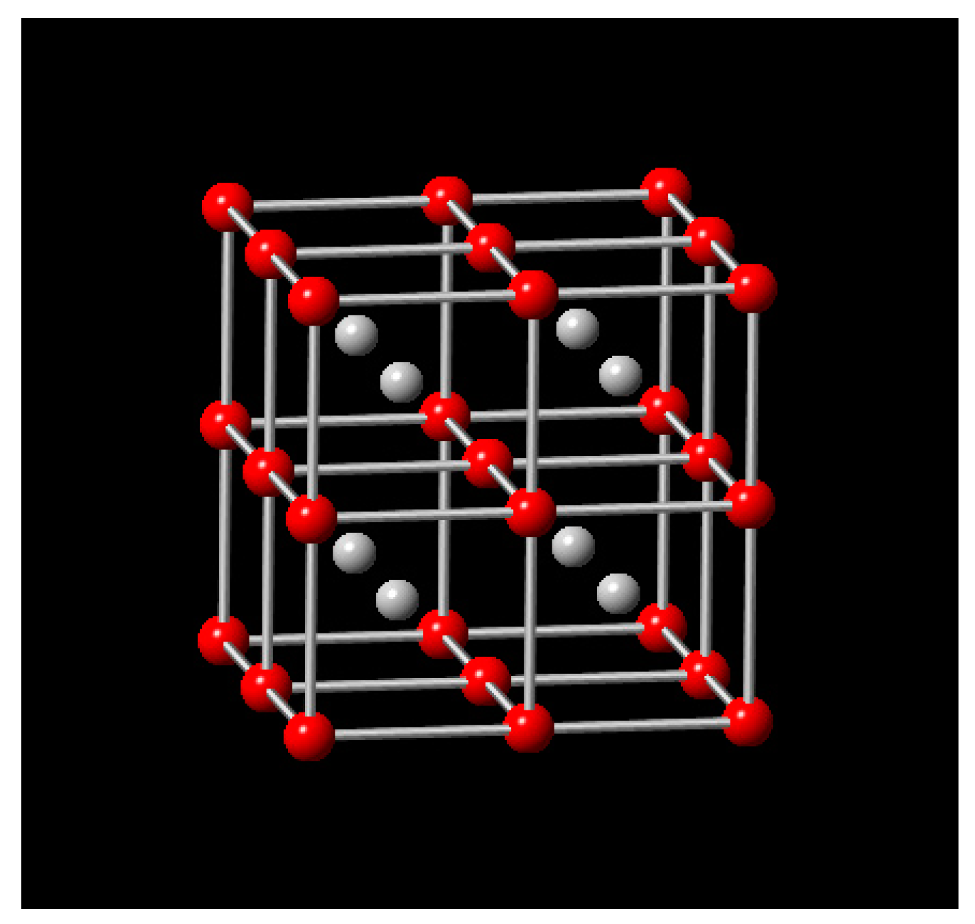
Figure 1. Schematic diagram of grid nodes of bilinear interpolation method for calculating interface curvature.
Crystals 10 00669 g001
Figure 2. Numerical simulation results of different interface energy anisotropy, α = 1.5; (a) k = 2; (b) k = 5.5; (c) k = 9.5; (df) are the corresponding cross sections of solid fraction.
Crystals 10 00669 g002
Figure 3. (a) Three-dimensional solid state rate results (b) x-z cross section equilibrium solid state rate and comparison of simulation and analytical solution (c) cross section of solid-liquid interface evolution.
Crystals 10 00669 g003
Figure 4. (a) Temperature distribution curve of 0° and 45° in x–z section and (b) velocity distribution scatter diagram of solid-liquid interface.
Crystals 10 00669 g004
Figure 5. Growth morphology of solid phase ratio of each 200 time steps: (ah).
Crystals 10 00669 g005
Figure 6. Three-dimensional facet temperature field and solid phase ratio profile.
Crystals 10 00669 g006
Figure 7. (a) Three-dimensional facet dendrite, (b) temperature field and solid-liquid interface morphology and (c) quarter enlarged view of dendrite.
Crystals 10 00669 g007
Table 1. Physical properties and calculation parameters used in the present model.
PropertyValue
Melting temperature, Tmel (T)1683
Density of silicon solid, ρs (kg·m−3)2330 − 2.19 × 10⁻²T
Density of silicon melt, ρm (kg·m−3)2330 − 2.19 × 10⁻²T − 1.21 × 10⁻⁵T2
Thermal diffusivity of silicon solid, as (m2/s)9.6 × 10−6
Thermal diffusivity of melt, a1 (m2/s)2.134 × 10−5
Molar liquid heat capacity, cp (j mol−1k−1)26.6
Molar melting entropy, Δsf (j mol−1k−1)29.8
Molar latent heat, ΔHf (j/mol)4.444 × 104
Liquidus slope, m (K/mass%)−0.7637