Abstract
Copper Sulfide (CuS) thin films were deposited onto a glass substrate using the Chemical Bath Deposition (CBD) technique. The chemical bath Precursors were made up of CuSO4, SC(NH2)2, and C4H6O6. Different parameters have been considered to specify the optimum conditions for fabricating CuS thin films, such as solution temperature, deposition time, pH level, and different precursor concentrations. It has been found that the optimum deposition time is 20 min at temperature 80 °C and pH = 11. The optimum precursor concentrations were 0.15 M, 0.2 M, and 0.1 M of CuSO4, SC(NH2)2, and C4H6O6, respectively. The structural properties of the thin film were studied using X-ray diffraction (XRD), and a single peak was observed for the thin film made at optimum conditions, while all other cases were amorphous. It is obvious from the optical characterization that the transmission spectra show a red-shift for the cases of increasing deposition time, bath temperature, C4H6O6 concentration, and pH. For the case of increasing CuSO4, blue shifts in the transmission spectra were observed. The energy band gap, resistivity, and activation energy of CuS thin films under optimum conditions are 2.35 eV, 0.7 Ω·cm, and 0.0152 eV, respectively.
1. Introduction
In recent years, transition metal chalcogenides have been increasingly studied due to their appropriate physical and chemical properties and potential for use in many industries. There are various techniques for the thin films to be prepared, such as pulsed laser deposition [1], electrodeposition [2], vacuum evaporation [3], chemical bath deposition [4], spray pyrolysis [5], successive ionic layer adsorption and reaction (SILAR) [6], and electron beam evaporation methods [7].
Among different metal chalcogenides, copper sulfide has been extensively studied and has attracted much interest in the recent research due to its special properties and potential applications such as in Solar cells [8], biomedical applications [9,10], photocatalysis [10], sensors [11], and as a cathode material in lithium chargeable batteries [12], etc. It is a binary inorganic chemical compound that occurs in nature as a dark indigo blue mineral, which has a general formula CuxSy. It is present in both synthetic materials and in minerals in the form of CuS (covellite) and Cu2S (chalcocite). Characterization and synthesis of CuS nanostructures have become an interesting area of research. It has been observed that CuS provides different absorbance edges both in the UV and visible regions [13].
The CBD is also called nucleation growth and is widely used in the laboratory for the deposition of chalcogenide semiconductors. It is a simple deposition technique requiring only a substrate to be placed in a vessel containing a supersaturated solution of dilute aqueous precursors such as metal salts, complexing agents, and pH buffers. It has many advantages, such as low-temperature operation, atmospheric pressure, low cost, and the ability to deposit large areas [14]. The deposition of CuS films was achieved from dilute solutions. Sulfide ions were released in the bath by the hydrolysis of Thiourea (SC(NH2)2), in the presence of OH− ions. Cu2+ ions were combined with the complex Ammonia (NH3). This ensured a slow release of Cu2+ ions in the solution [15]. In this work, the chemical bath deposition technique has been used to prepare CuS thin films, studying different parameters (solution temperature, deposition time, pH level and different precursor’s concentration) to specify the optimum conditions for fabricating CuS thin films, and investigating the structure, optical, and electrical properties suitable for photovoltaic solar cell applications.
2. Methodology and Characterization
Glass Substrates of size (25 × 75 × 1 mm) were used to deposit CuS thin films. The substrates were soaked in Chromic Acid for 24 h then cleaned with distilled water, rinsed in Ethanol. Furthermore, substrates were ultrasonically cleaned with distilled water and dried in air and kept in a desiccator.
CuS was prepared using 20 mL of each 0.1 M Copper Sulphate (CuSO4), 0.1 M Tartaric Acid (C4H6O6), and Thiourea (SC(NH2)2) using a chemical bath deposition technique in an alkaline solution. Different bath compositions were used to prepare solutions, as shown in Table 1. The solution is stirred for a few min to get a homogeneous mixture. The CBD solution color changed during the time from blue to dark indigo blue color, which indicates the formation of CuS as shown in Figure 1, where the pH was adjusted to 10 by adding an appropriate amount of Ammonia solution at first. Slides were soaked in the prepared solution at a small angle with the vertical.

Table 1.
Chemical baths.

Figure 1.
Different stages of chemical bath solution with time where (a) represents the CBD solution of CuSO4, SC(NH2)2, and NH4OH. (b) Immediately after adding C4H6O6 to the CBD solution. (c) After 20 s of adding; (d) after 1 min; (e) after 2–3 min.
The electrical resistivity was investigated by I-V characteristics. Aluminum electrodes were evaporated on the surface of CuS films using the physical vapor deposition technique [16].
The activation energy of the CuS thin films was investigated by studying the variation of conductivity with the temperature of the film under vacuum (10−1 mbar).
The thickness of the thin films was measured using the optical interferometer technique, where thickness (d) is calculated by the below formula.
where λ is the wavelength of the He-Ne laser (632.8 nm), is the distance between two fringes, and is the fringe width [17].
Structure properties were studied using the X-ray diffraction system X-Pert Pro PANalytical with a scanning range of 2Theta set between 20° and 70°, with a wavelength of 1.5406 Å from CuKα operating at 40 kV, 30 mA.
The optical transmittance spectra of the CuS thin films were recorded by the UV-VIS Spectrophotometer in the range of 200–1100 nm.
The direct energy gap of the thin films is calculated from the Tauc’s equation as shown below:
where α is the absorption coefficient that is given by (α = 2.303 log (T/d)), A is the absorption, hυ is the incident photon energy, Eg is the bandgap energy, T is the transmittance, and d is the film thickness [18].
The electrical properties of the CuS thin films were measured from the I-V characteristic curve using (KEITHLEY 2450) and the electrical resistivity of the deposited films was determined by the equation:
where R is the sheet resistance, ρ is the resistivity of the thin film, L is the length between two probes, and A is the cross-sectional area of the probes [19].
The activation energy of the thin films was calculated by the Arrhenius Equation [20,21].
where σ is conductivity, A is the pre-exponential factor, Ea represents activation energy, KB is Boltzman constant, and T is absolute temperature [22].
3. Results and Discussion
3.1. Thickness and Growth Rate
It can be seen that at certain temperatures CuS could be precipitated either in the bath solution with the formation of colloids or at the surface of the immersed substrate in the solution. The formation of CuS layers occurs when the ionic product of Cu2+ and S2− exceeds the solubility product of CuS (Ksp = 5 × 10−36) [23].
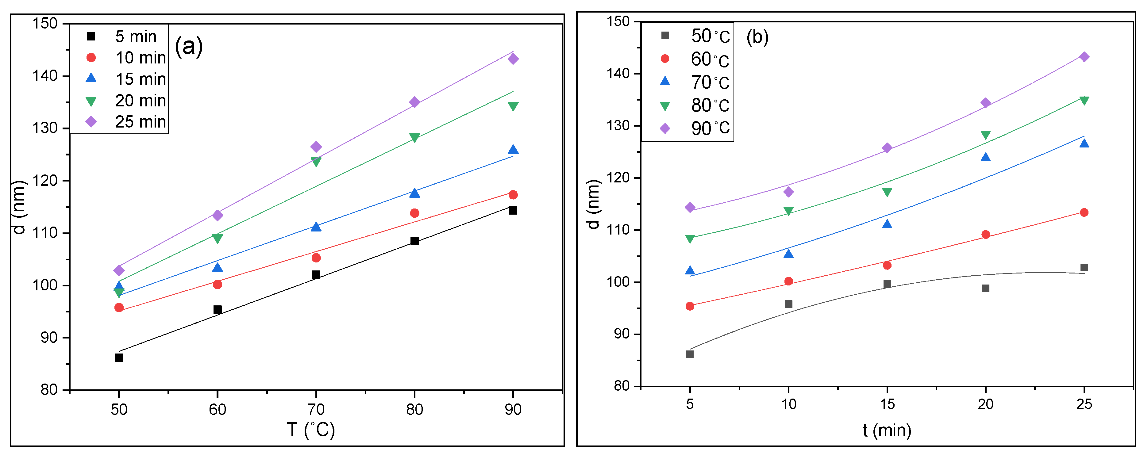
Figure 2a,b shows the thickness of CuS thin films as a function of deposition temperature and deposition time, respectively. The curves in Figure 2a show a linear increase of film thickness with the deposition temperature at specific deposition time, with no indication of saturation. Figure 2b shows the thin film thickness as a function of deposition time. From the figure, one can notice that at 50 °C it reached saturation at 15 min of deposition time, while at higher deposition temperature it is not reached even at 25 min of deposition time [23,24].
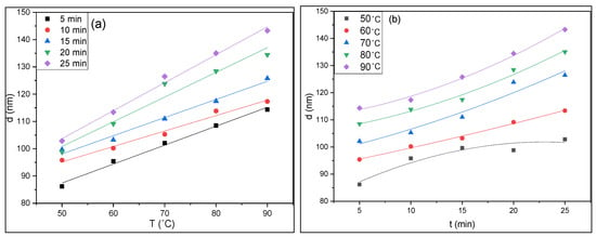
Figure 2.
Thickness of CuS films as a function of (a) temperature at different deposition times and (b) deposition time at different temperatures at [CuSO4] = 0.1 M, [SC(NH2)2] = 0.1 M, [C4H6O6] = 0.1 M, and pH = 10.
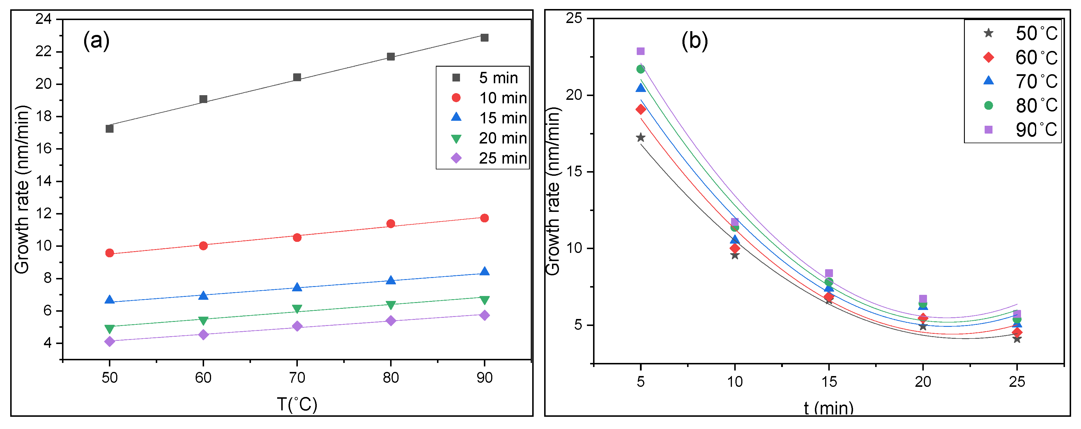
Figure 3a,b shows the growth rate of CuS deposition thin films. Figure 3a indicates the growth rate of CuS thin film as a function of deposition temperature at constant deposition time. From the figure, it can be seen that the deposition growth rate gradually increases with deposition temperature and this is due to more generation of colloidal ions. The growth rate is decreasing with the increasing deposition time at a constant deposition temperature due to precursor consumption over time, as shown in Figure 3b [4].
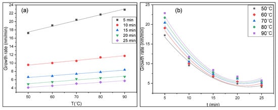
Figure 3.
Growth rate variation as a function of (a) temperatures at different deposition times and (b) deposition time at different temperatures, at [CuSO4] = 0.1 M, [SC(NH2)2] = 0.1 M, [C4H6O6] = 0.1 M, pH = 10.
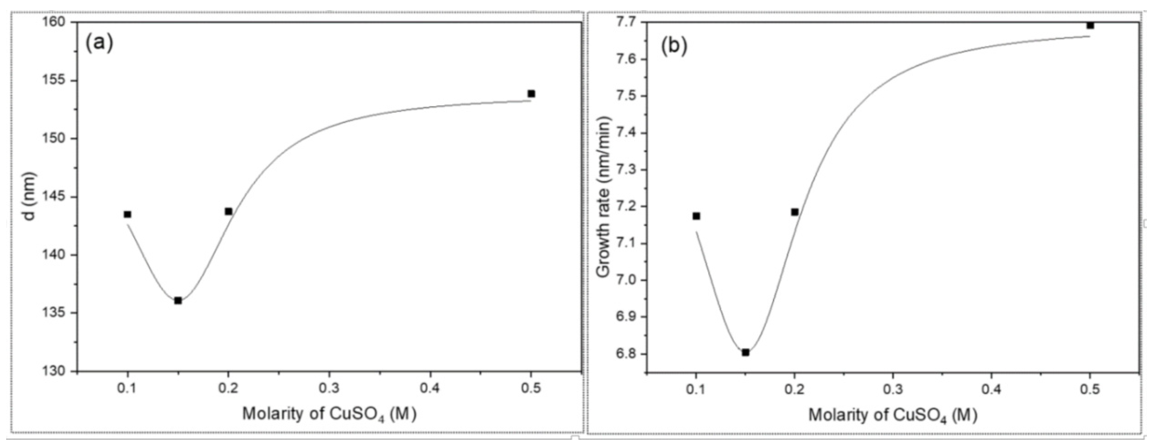
Figure 4a,b shows the effect of different CuSO4 precursor concentration on the thickness and growth rate of CuS thin films, respectively. Figure 4a shows that the thickness of CuS films decreases from 148 to 136 nm as the CuSO4 concentration increases from 0.1 M to 0.15 M [25]. The deposition on a substrate mainly depends on the formation of nucleation sites and subsequent growth of the thin films from the center. Hence, irregularly shaped grains with different sizes are observed on the surface of the film. The film thickness almost increases exponentially with the increase from 136 nm to 152 nm in the concentration of copper ions from 0.15 M to 0.5 M. Depositions with concentrations above 0.1 M result in the formation of outer porous layer stress which tends to cause delamination, resulting in peeling off the film [26]. Furthermore, the competition of heterogeneous nucleation on the substrate and homogeneous nucleation in the solution [25] would alter the growth of the thin film, and here the thickness increased again. The surface morphology of the film deposited at 0.15 M is quite uniform and well covered on the substrate when compared with the other concentrations using the optical microscope [24].
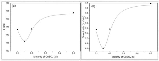
Figure 4.
The effect of copper ion concentrations on (a) the thickness, (b) the growth rate of CuS thin film at a temperature of 80 °C and deposition time 20 min with pH = 11 and precursor concentrations at [SC(NH2)2] = 0.1 M, [C4H6O6] = 0.1 M.
An increase in growth rate with CuSO4 concentration is observed from Figure 4b. The induction time also becomes shorter at a higher CuSO4 concentration. In order to determine the apparent reaction orders, the growth rate is assumed to be dependent on the variation of initial reagent concentration during the initial linear growth region [24].
Figure 5 shows the growth rate of CuS thin films as a function of C4H6O6 concentration. The thicknesses of the films depend strongly on the molarity of the C4H6O6, where the thickness increases as the concentration is increased. Copper ions (Cu2+), introduced into the solution as copper salts, can form different complex species with complexing agents such as tartaric acid and ammonia. Appropriate complexing agents are present to produce a stable complex of Cu2+ ions in the solution in which Cu2+ ions are slowly released on dissociation, resulting in a controllable reaction rate. For a metal M and complexing agent, A, the existence of free metal ions in the solution can be expressed by the equilibrium reaction [24].
M(A)2+ ↔ M2+ + A
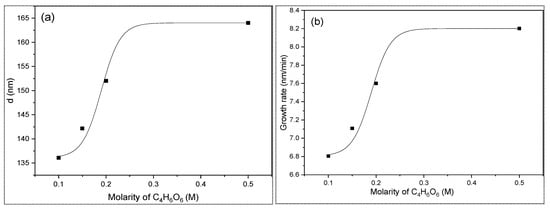
Figure 5.
The effect of C4H6O6 concentration on the (a) thickness, (b) growth rate of CuS thin films at a temperature of 80 °C, deposition time of 20 min, and pH = 11.
It has been seen that a saturation region occurs at higher concentrations of C4H6O6, which is clearly defined in Figure 5.
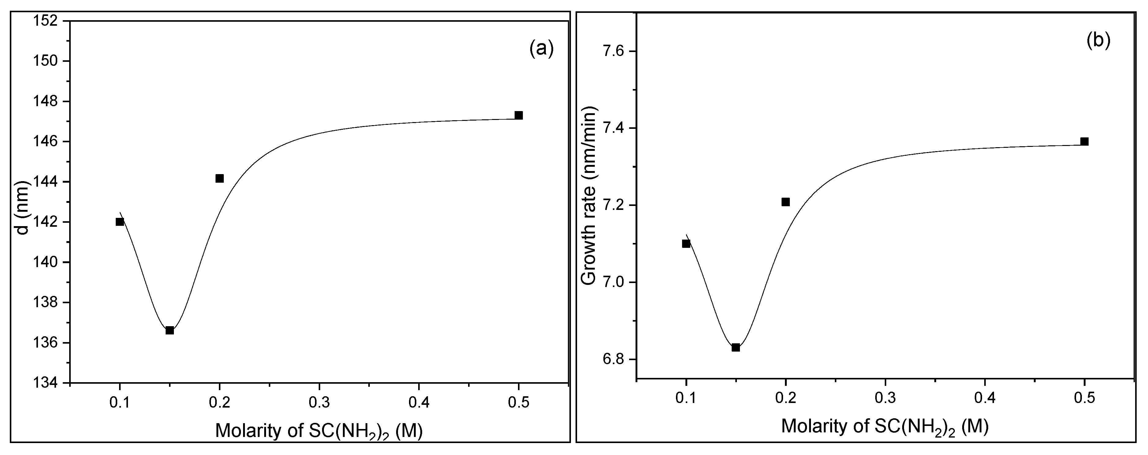
Figure 6a,b shows the influence of the thiourea concentration on the film thickness and the growth rate of CuS thin films. An increase of the initial growth rate with the SC(NH2)2 concentrations is observed; such an increment can be attributed to the increase in the number of S2 in the thiourea volume, which accelerates the reaction forming CuS [27] and has good agreement with the work of Reference [24].
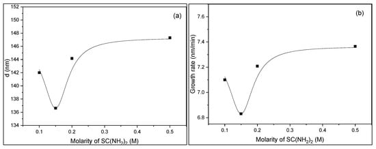
Figure 6.
The influence of the SC(NH2)2 concentration on CuS thin film. (a) Thickness, (b) growth rate at a temperature of 80 °C and deposition time of 20 min with pH = 11 and precursor concentrations at [CuSO4] = 0.15 M, [[C4H6O6]] = 0.2 M.
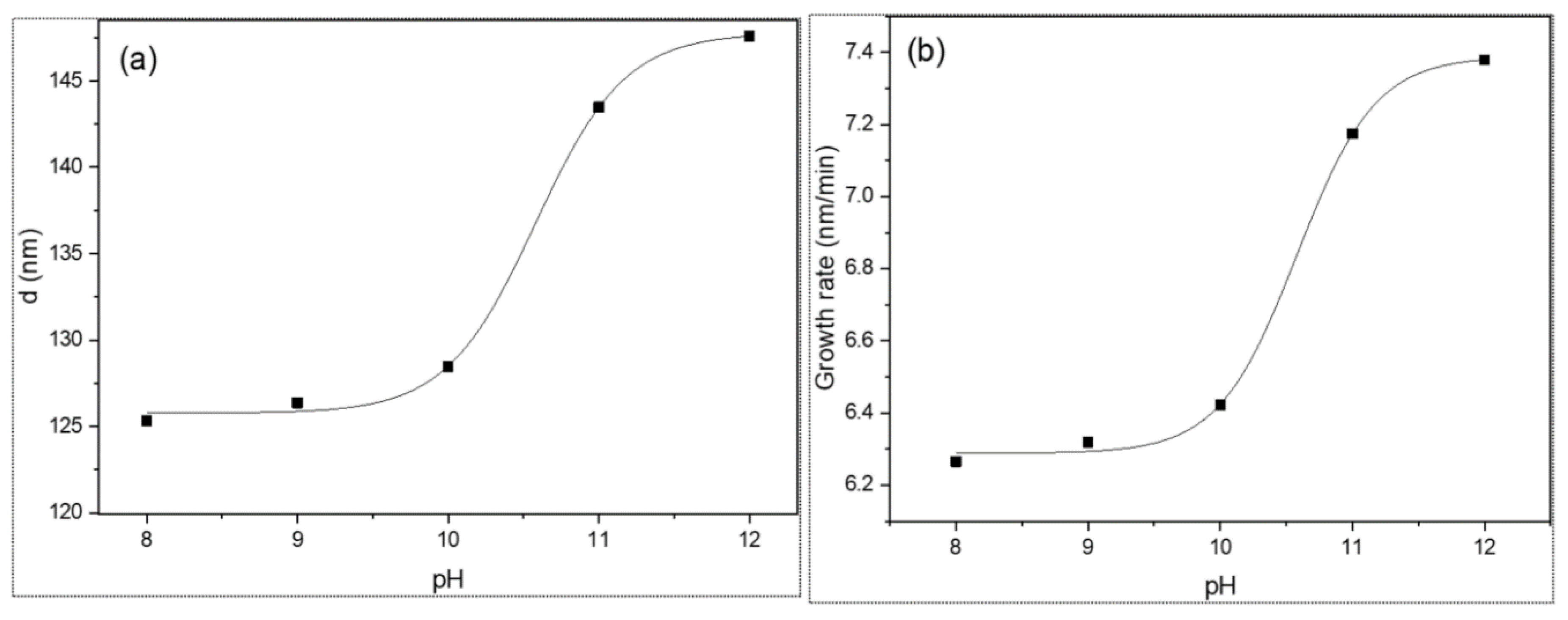
Figure 7 shows a significant change of the thin film thickness with respect to different pH rates; the thickness of the thin film increases as the pH rate increase [28], and an increase in pH value leads to a higher film growth rate. A higher concentration of OH− ions in the solution will push the reaction of thiourea hydrolysis forward, and hence a higher generation of sulfide ions has occurred. In Reference [29], the optimum pH was found to be 11, and in Figure 7 we see that at pH = 12 the thickness was higher but the thin film morphology was not uniform and little cracks were seen on the thin film surface when using an optical microscope [15].
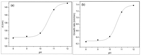
Figure 7.
The effect of pH on the CuS thin film. (a) Thickness, (b) growth rate at a temperature of 80 °C and a deposition time of 20 min.
Figure 8 shows that the samples prepared at a deposition temperature (80 °C), pH 11, and precursor concentrations of 0.1 M CuSO4, 0.2 M C4H6O6, and 0.1 M SC(NH2)2 at different deposition times (15, 20, and 25 min). Figure 8 shows that the film fabricated at the 20 min deposition time has more homogeneity over the entire film area without any cracks. The film prepared at 15 min of deposition time has voids and is not smooth. The film prepared at 25 min deposition time has many cracks and is not a continuous film. Based on the above, 20 min of deposition time has been considered as the optimum deposition time.

Figure 8.
Pictures from the optical microscope for different samples made with different deposition times of (a) 15 minutes, (b) 20 minutes, and (c) 25 minutes.
3.2. Structure Properties of CuS Thin Films
Figure 9 shows the XRD patterns of CuS thin films prepared at different deposition times (5, 10, 15, 20, and 25 min), at a constant bath temperature of 80 °C, pH = 10, and precursor concentrations of 0.1 M CuSO4, 0.1 M C4H6O6, and 0.1 M SC(NH2)2. From the figure, one can notice that all the deposition times with the above parameters give an amorphous structure.
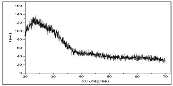
Figure 9.
The XRD pattern of CuS thin film deposited at different deposition times at a constant bath temperature 80 °C, pH = 10, and precursor concentrations of [CuSO4] = 0.1 M, [SC(NH2)2] = 0.1 M, and [C4H6O6] = 0.1 M.
Figure 10 reveals the XRD patterns of a CuS thin film fabricated at different deposition temperatures (50, 60, 70, 80, and 90 °C), a deposition time 20 min, pH = 10, and precursor concentrations of 0.1 M CuSO4, 0.1 M C4H6O6, and 0.1 M SC(NH2)2. Also, all the samples prepared with the above parameters give an amorphous structure.
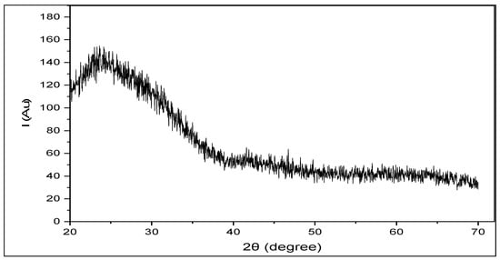
Figure 10.
XRD pattern of the CuS thin film deposited at different temperatures at a time of 20 min, pH= 10, and precursor concentrations of [CuSO4] = 0.1 M, [SC(NH2)2] = 0.1 M, and [C4H6O6] = 0.1 M.
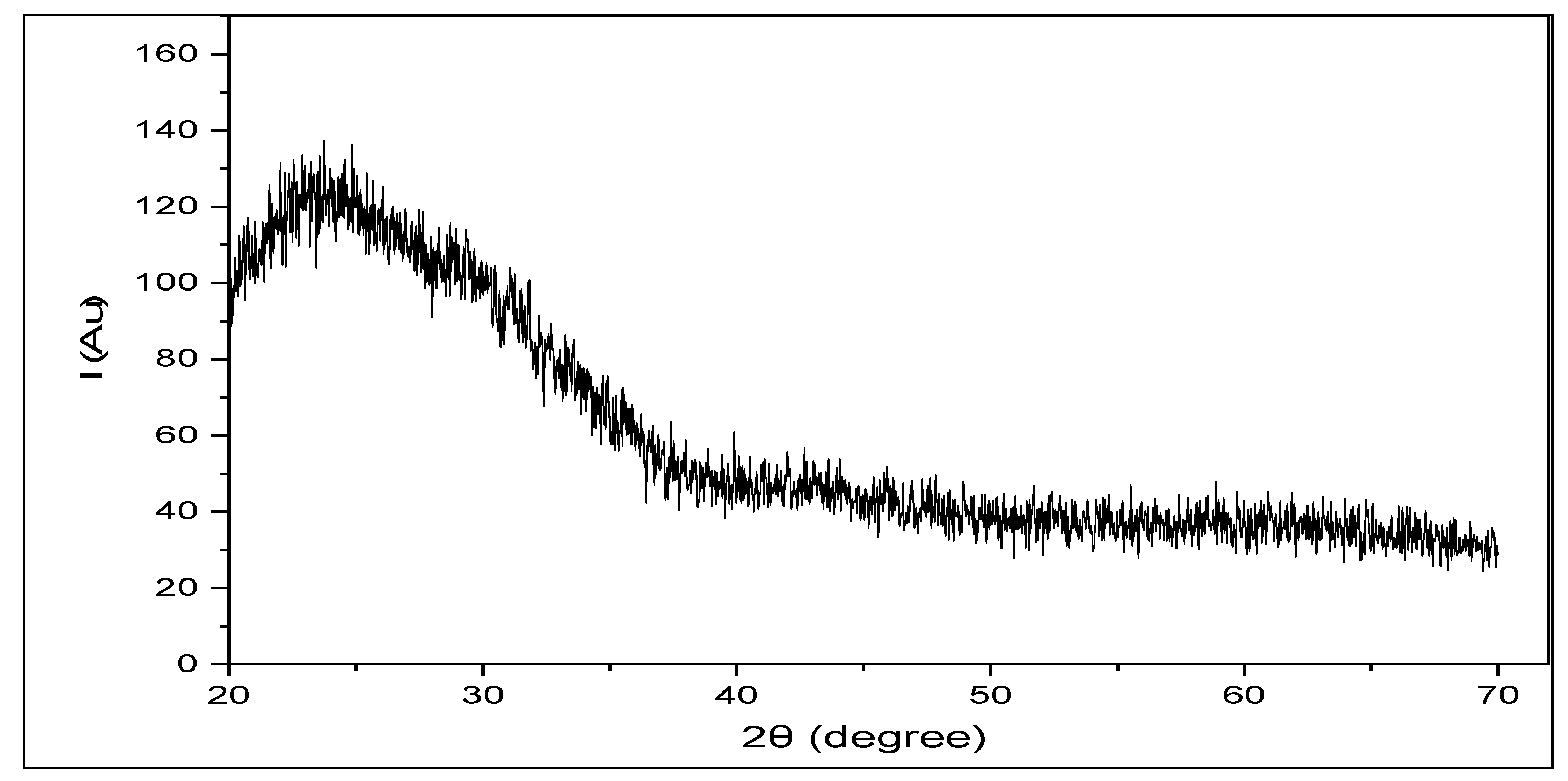
Figure 11 represents the XRD patterns of CuS thin films deposited at different pH (8, 9, 10, 11, and 12), a deposition time of 20 min, a deposition temperature of 80 °C, and precursor concentrations of 0.1 M CuSO4, 0.1 M C4H6O6, and 0.1 M SC(NH2)2. It gives the same result, which is an amorphous structure for all samples prepared with the above parameters.
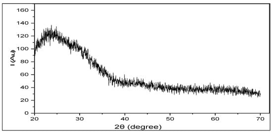
Figure 11.
The XRD pattern of the CuS thin film deposited at different pH rates and a constant time of deposition of 20 min, a bath temperature of 80 °C, and at precursor concentrations of [CuSO4] = 0.1 M, [SC(NH2)2] = 0.1 M, and [C4H6O6] = 0.1 M.
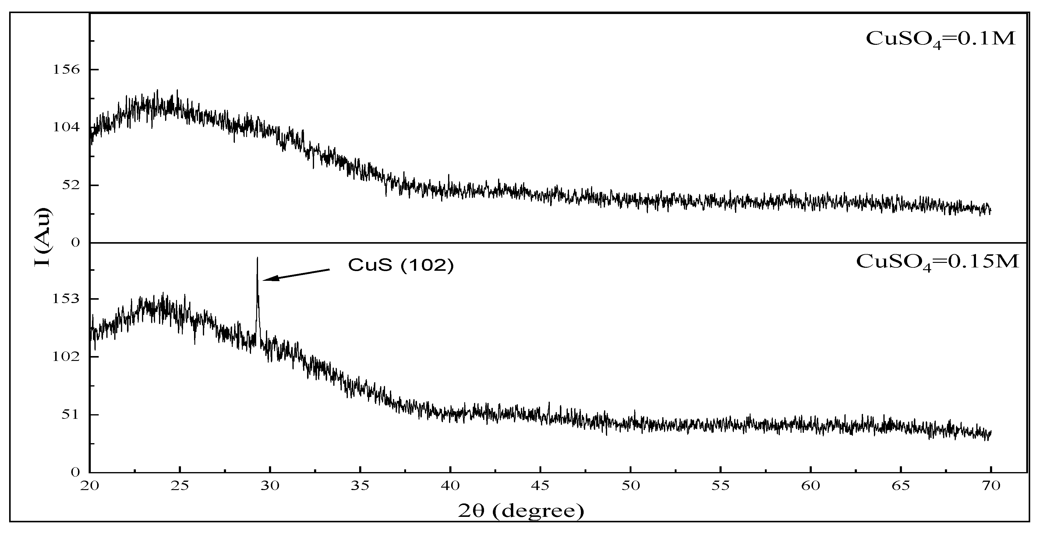
Figure 12 reveals the XRD pattern with respect to different concentrations of CuSO4 (0.1 and 0.15 M), at a constant time of deposition of 20 min, a bath temperature of 80 °C, and precursor concentrations of 0.1 M C4H6O6, and 0.1 M SC(NH2)2, and pH = 11. From the figure, it can be seen that 0.1 M CuSO4 gives an amorphous structure and 0.15 M CuSO4 gives a crystalline structure. Also, one can conclude that as the concentration increases, the crystalline nature of the thin film increases. This result was also reported by Sangamesha et al. [25,30].

Figure 12.
The XRD pattern of the CuS thin film deposited with different concentrations of CuSO4 at a constant time of deposition of 20 min, a bath temperature of 80 °C, and precursor concentrations of [SC(NH2)2] = 0.1 M, [C4H6O6] = 0.1 M, and pH = 11.
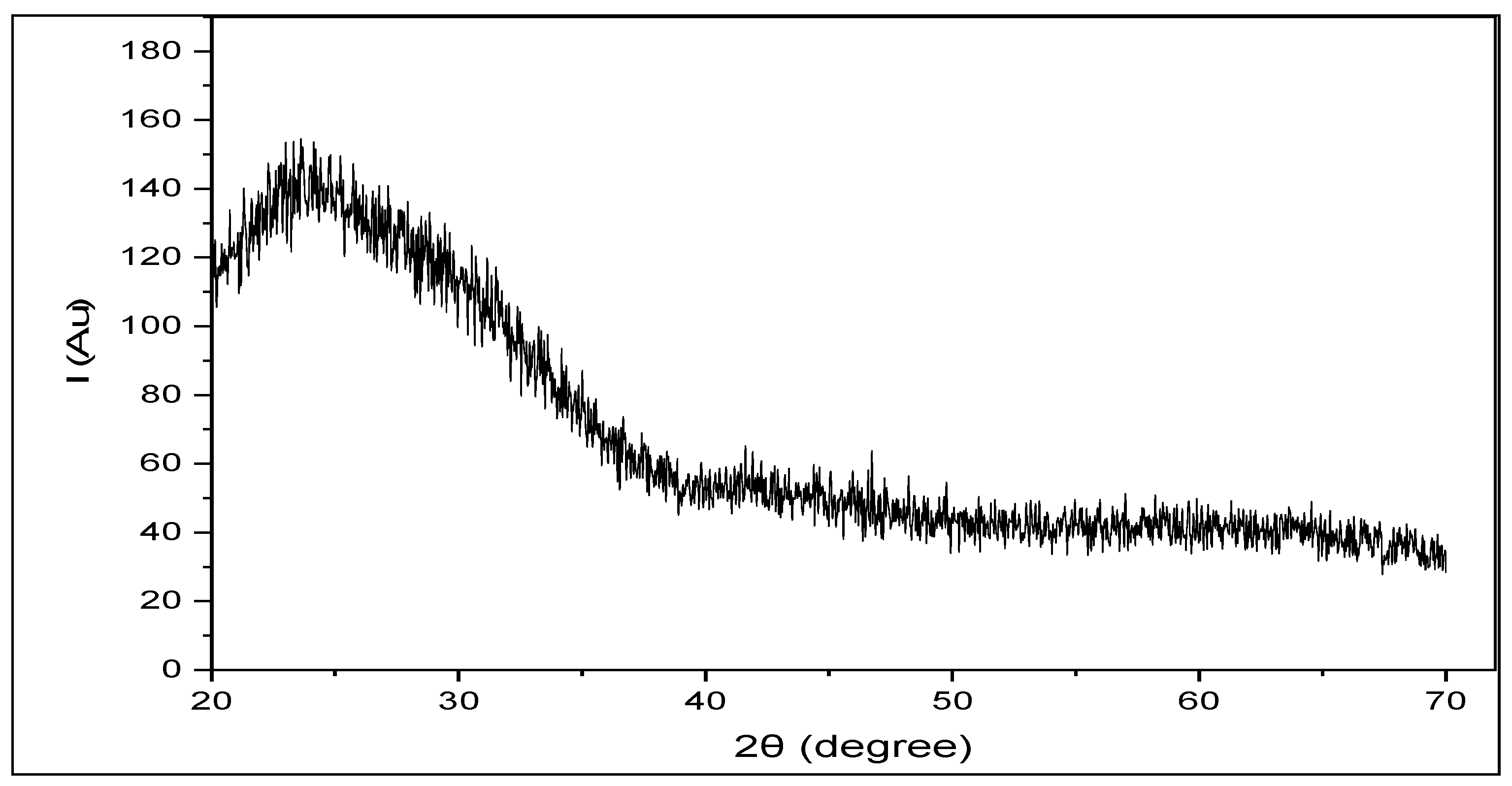
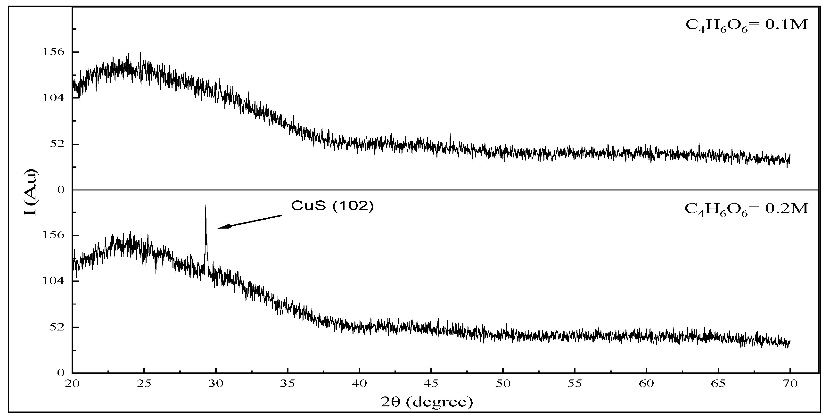
Figure 13 represents the XRD patters with respect to the different concentrations of C4H6O6 (0.1 and 0.2 M), at a constant time of deposition of 20 min, a bath temperature of 80 °C, precursor concentrations of 0.15 M CuSO4 and 0.1 M SC(NH2)2, and pH = 11. From the figure, it can be noticed that 0.1 M C4H6O6 gives an amorphous structure, while 0.2 M C4H6O6 gives a crystalline structure.
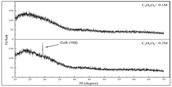
Figure 13.
The XRD pattern of the CuS thin film deposited with different concentrations of C4H6O6 at a constant time of deposition of 20 min, a bath temperature of 80 °C and precursor concentrations of [SC(NH2)2] = 0.1 M, [CuSO4] = 0.15 M, and pH = 11.
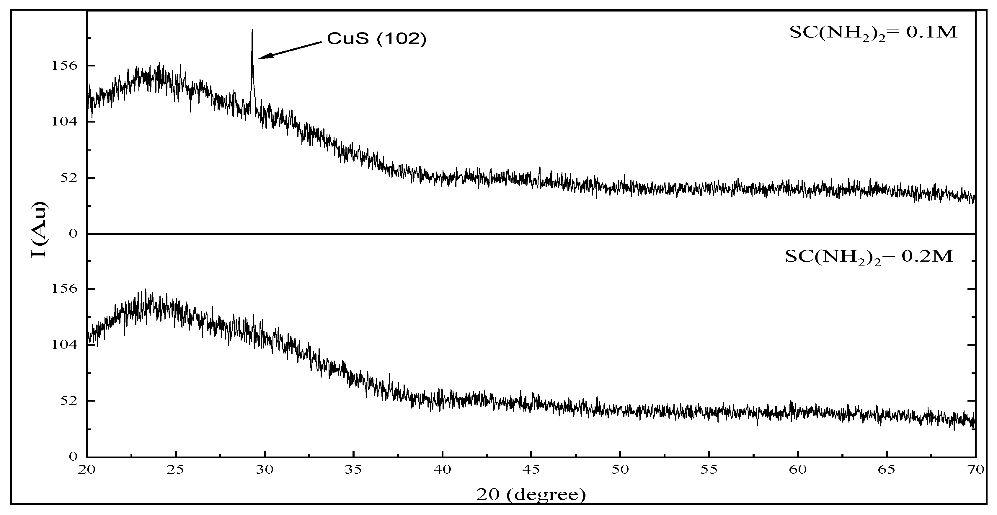
Figure 14 shows the XRD pattern of different SC(NH2)2 concentrations (0.1, and 0.2 M) at a constant time of deposition 20 min, a bath temperature of 80 °C, and precursor concentration of 0.15 M CuSO4, 0.2M C4H6O6, and pH = 11. From the figure, one can conclude that the 0.1 M SC(NH2)2 gives an amorphous structure, while 0.2M SC(NH2)2 gives a crystalline structure.

Figure 14.
The XRD pattern of the CuS thin film deposited with different concentrations of SC(NH2)2 at a constant time of deposition of 20 min, a bath temperature of 80 °C, and precursor concentrations of [C4H6O6] = 0.2 M, [CuSO4] = 0.15 M, and pH = 11.
From above study of the structure and morphology of the films, the authors considered the following parameters (a deposition time of 20 min, deposition temperature of 80 °C, pH = 10, and precursor concentrations of [CuSO4] = 0.1 M, [SC(NH2)2] = 0.1 M, and [C4H6O6] = 0.1 M) are the optimum parameters.
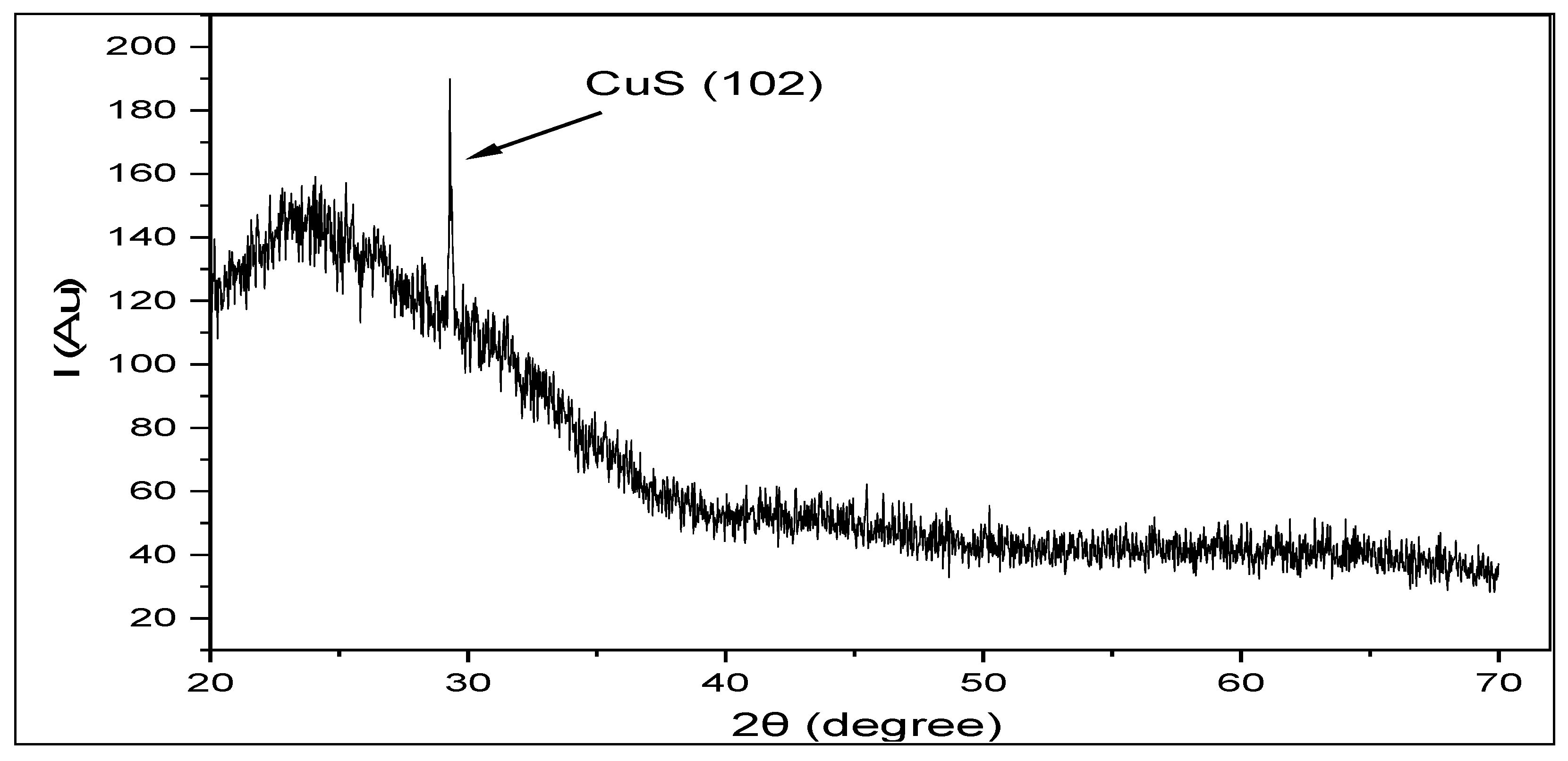
Figure 15 reveals the XRD pattern of the CuS thin film prepared at the optimum conditions. From the figure, one can notice that there is a single peak appearing at (2θ = 29.31°). This peak position coincides with the information of the Joint Committee on Powder Diffraction Standard data (JCDPS), chart No. (1040), belonging to the CuS hexagonal crystal structure compound with the preferred orientation (102), and this result agrees with others [4,29,31]. The calculated lattice constants are (a = b = 3.85 Å, c = 16.26 Å, d = 3.044 Å, α = 90°, β = 90°, γ = 120°).

Figure 15.
The XRD pattern of the CuS thin film deposited under the optimum conditions with deposition for 20 min at a constant bath temperature of 80 °C, pH =11, and precursor concentrations of [CuSO4] = 0.15M, [SC(NH2)2] = 0.2 M, and [C4H6O6] = 0.1 M.
3.3. Optical Properties of CuS Thin Films
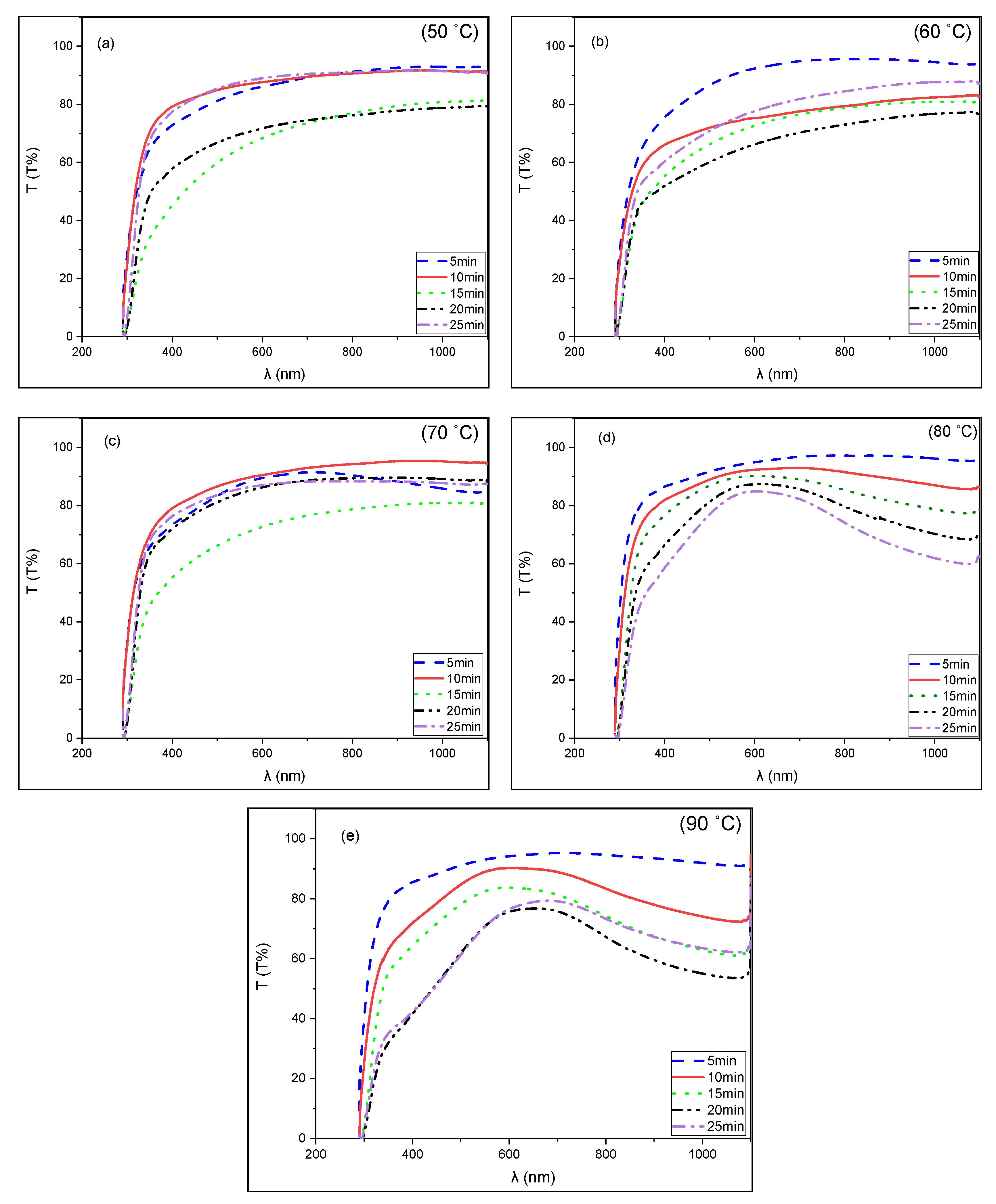
The transmittance of CuS thin films is studied for thin films prepared at different deposition times and temperatures at pH 10, and precursor concentrations of 0.1 M CuSO4, 0.1 M SC(NH2)2, and 0.1 M C4H6O6.
Figure 16 shows the transmittance of CuS thin films as a function of wavelength prepared at different deposition times at constant deposition temperatures. Strong regions of the absorption edge can be notices in the range of 300 to 340 nm for all samples.
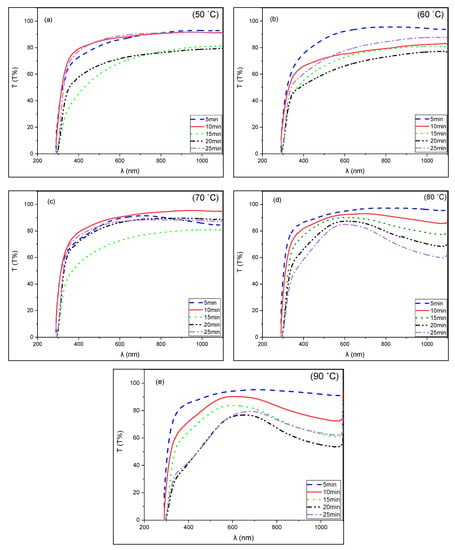
Figure 16.
Optical transmission spectra of CuS thin films at different deposition times with temperatures (a) 50 °C, (b) 60 °C, (c) 70 °C, (d) 80 °C, and (e) 90 °C, with respect to wavelength at pH = 10, and precursor concentrations of [CuSO4] = 0.1 M, [SC(NH2)2] = 0.1 M, and [C4H6O6] = 0.1 M.
From Figure 16d, the transmittance decreases with increasing deposition time, and this is coinciding with thin film thickness, as shown in Figure 2. One can see that the maximum transmittance is (96%) and decreases to (83%) in the visible region. In Figure 16e, we can see that at 25 min of deposition time, transmittance is higher than at 20 min. This is due to the peeling of the film from the surface.
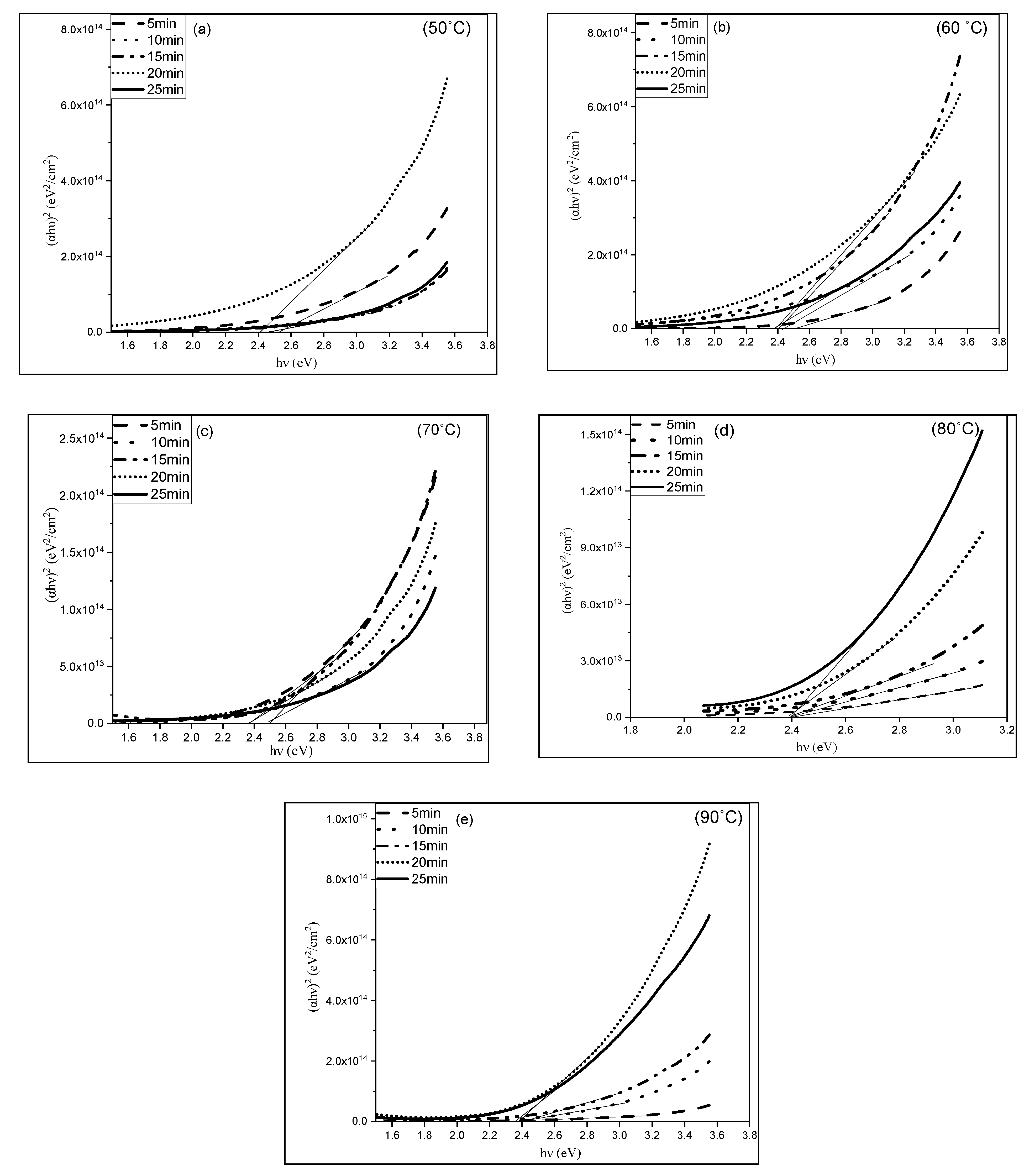
The energy bandgap (Eg) of CuS is direct [32] Figure 17 represents the relation between (αhν)2 and photon energy hν for different deposition times. From the extrapolation of the above relation in Figure 17, energy band gaps are determined.

Figure 17.
The relationship between (αhν)2 against hν for different deposition times at deposition temperatures of (a) 50 °C, (b) 60 °C, (c) 70 °C, (d) 80 °C, and (e) 90 °C.
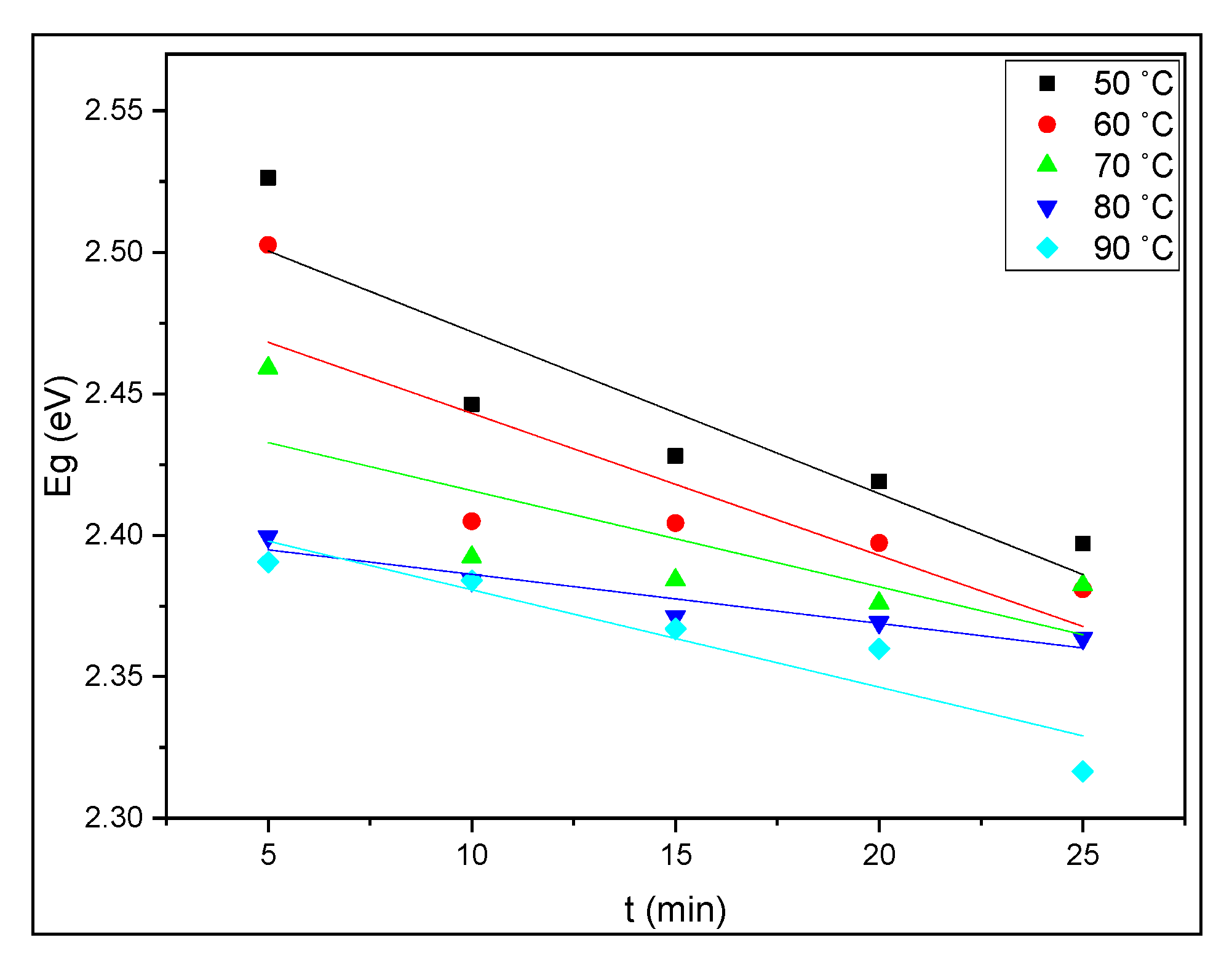
Figure 18 shows the relation between the energy bandgap and deposition time at constant temperature. The maximum energy band gap is 2.399 eV at a deposition time of 5 min, and the minimum energy bandgap is 2.363 eV at a deposition time of 25 min, which indicates that the energy band gap decreased with the increase of the grain size of the film.
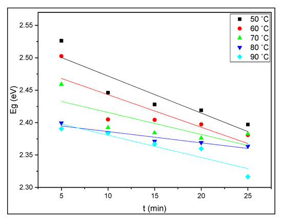
Figure 18.
The relationship between the energy band gap and deposition time at a constant deposition temperature.
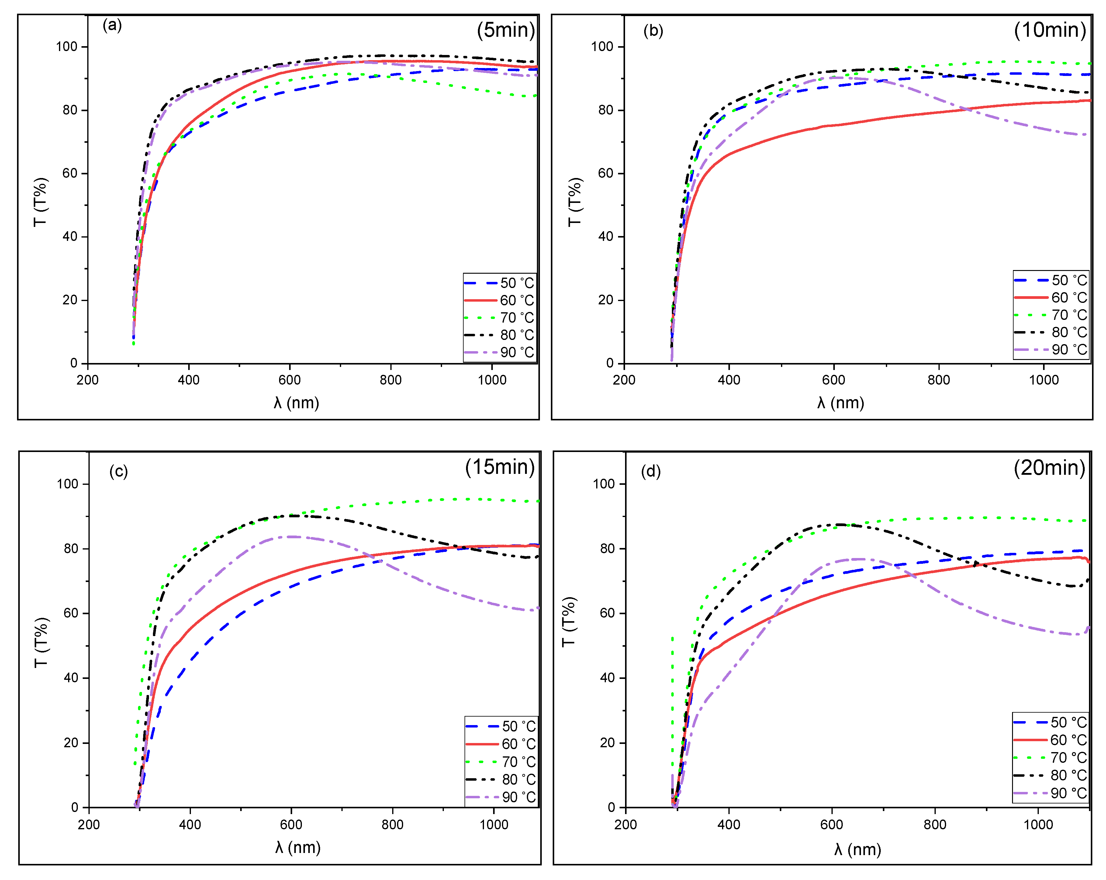
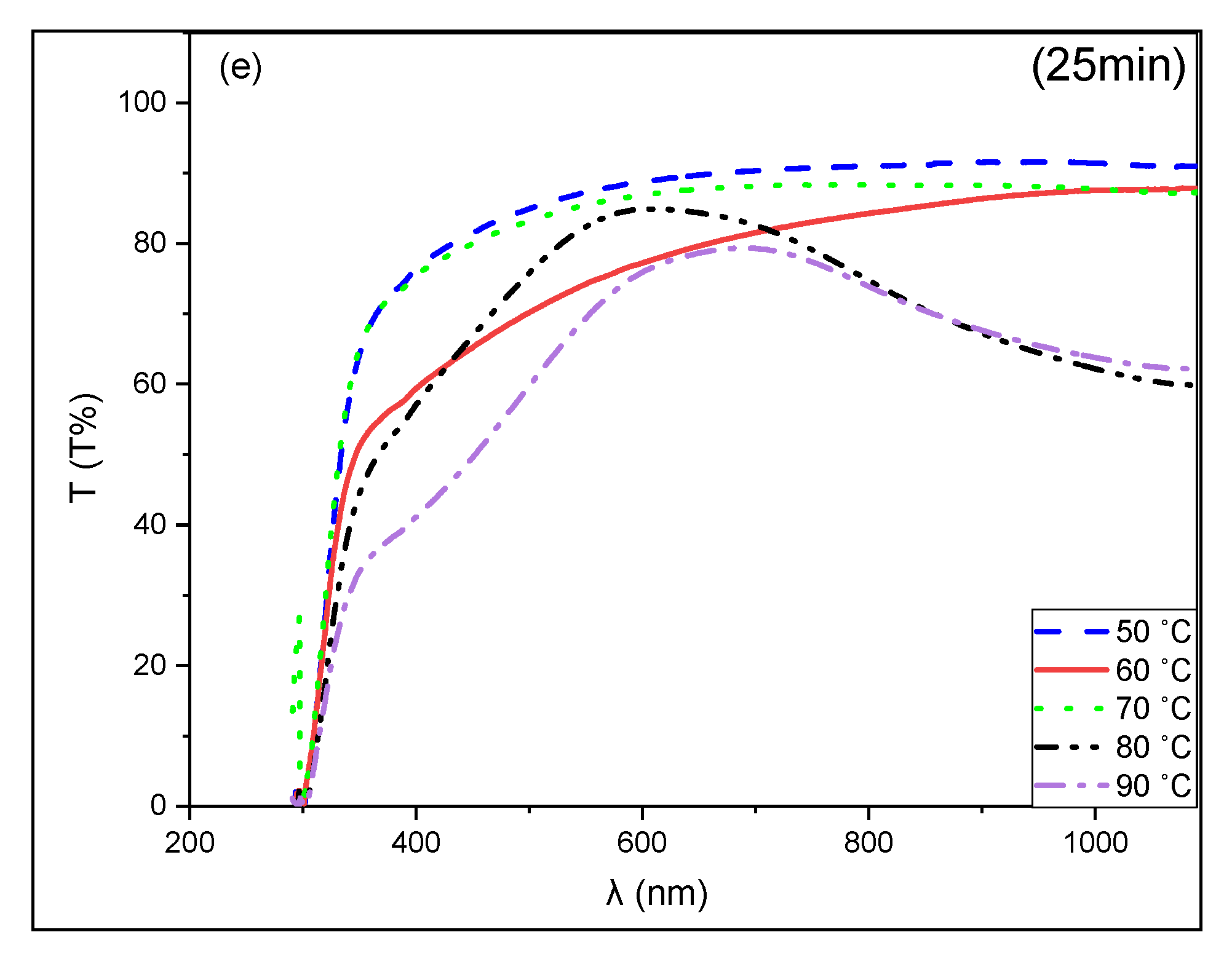
Figure 19 indicates the optical behavior of the case at different deposition temperatures. In Figure 19d, a significant difference in the behavior of the transmission line is noticed, and for temperatures of 50, 60, and 70 °C the transmission is higher at the IR region and slowly comes down until reaching the 300 nm wavelength and sharply becomes zero at this point. However, in the higher temperature of the solution, the behavior changes, and for 90 °C the low range of the transmission is shown in the IR region and slowly becomes higher until it reaches the peak at 650 nm and then sharply reduces to zero at 300 nm. Although the influence of the increase of the number of free carriers cannot be ruled out, it is more likely that this effect results from the increase in the film roughness with thickness [27]. This is a good indicator that the films are strong absorbers in the visible region [33].
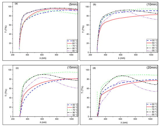
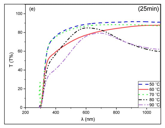
Figure 19.
Optical transmission spectra of CuS thin films at different deposition temperatures with deposition times of (a) 5 min, (b) 10 min, (c) 15 min, (d) 20 min, and (e) 25 min, with respect to wavelength at pH = 10, and precursor concentrations of [CuSO4] = 0.1 M, [SC(NH2)2] = 0.1 M, and [C4H6O6] = 0.1 M.
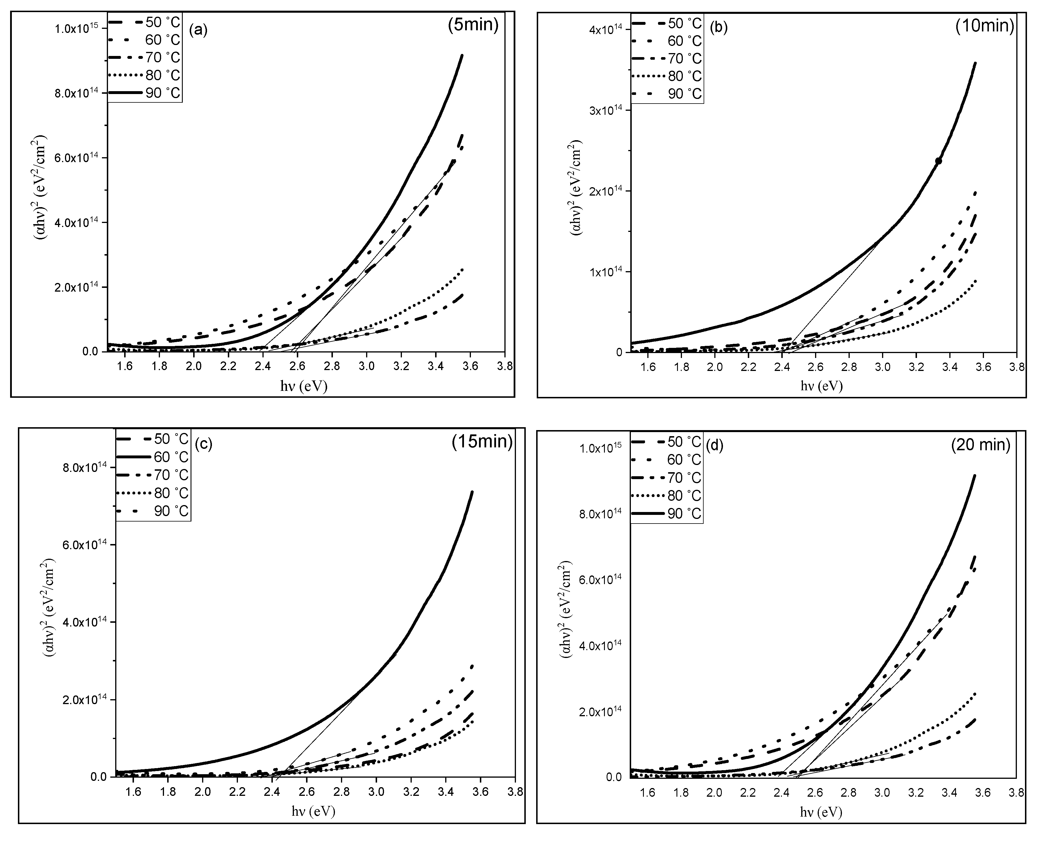
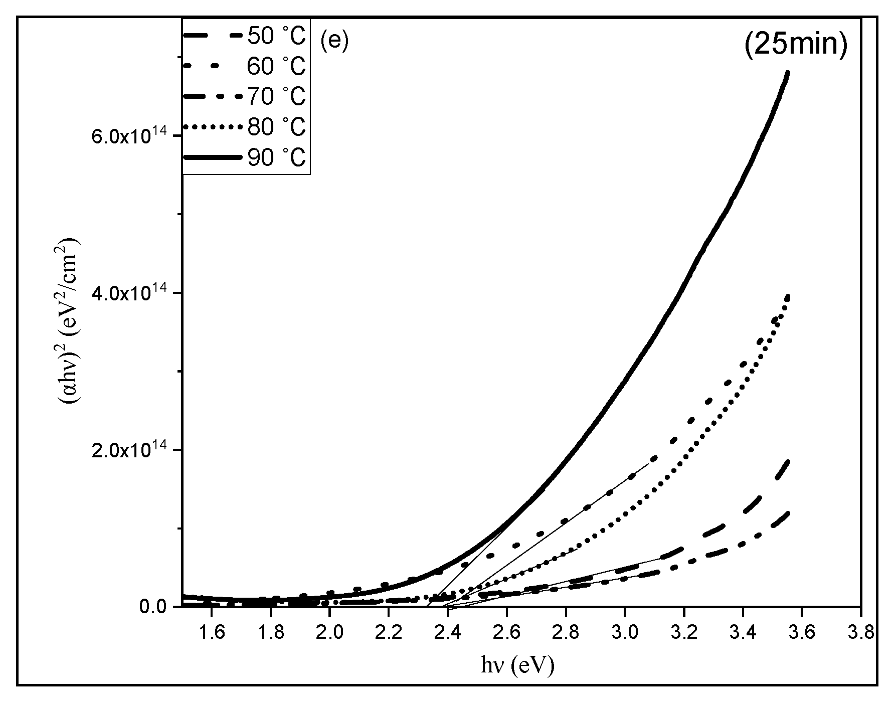
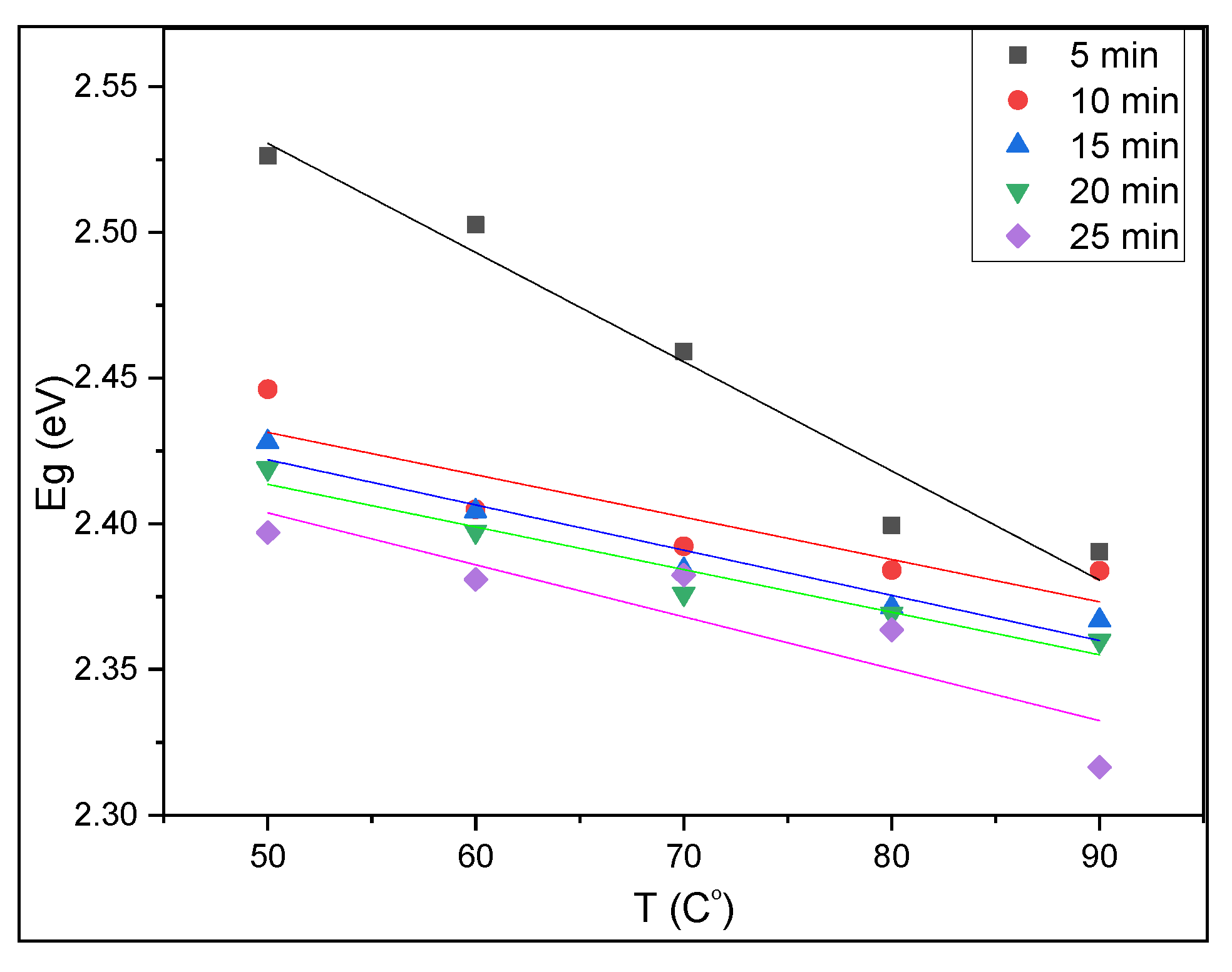
Figure 20 and Figure 21 represent the relationship between photon energy hν and (αhν)2 for different bath temperatures at a constant deposition time and the relationship between the energy gap and temperature, respectively. A reverse relationship can be seen between both the deposition temperature and energy gap, and for a constant deposition time of 5 min a sharper decrease is shown in the energy gap for the bath temperatures of 50, 60, 70, 80, and 90 °C, found to be 2.41, 2.39, 2.37, 2.36, and 2.35 eV, respectively. The bandgaps were decreased due to the fact that the transmission is strongly dependent on the thickness and surface conditions [33,34].
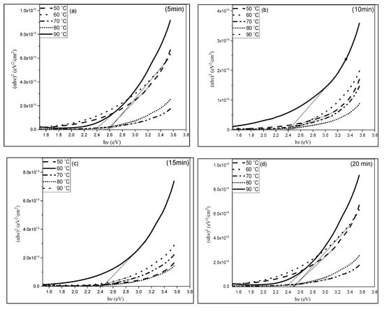

Figure 20.
The relationship between (αhν)2 against hν for different deposition temperatures at a deposition time of (a) 5 min, (b) 10 min, (c) 15 min, (d) 20 min, and (e) 25 min.
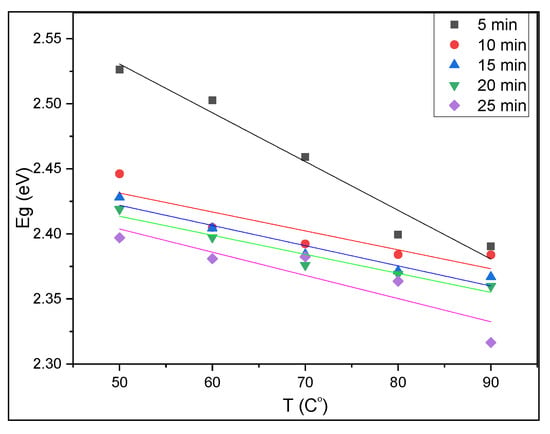
Figure 21.
The relationship between the energy band gap and deposition time at a constant deposition temperature.
The relationship between energy bandgap with respect to the time of deposition is shown in Figure 21. At 5 min of deposition time, a larger decrease of the energy gap can be noticed because the initial growth of the film at 5 min of deposition time was faster according to Figure 2a [31,34].
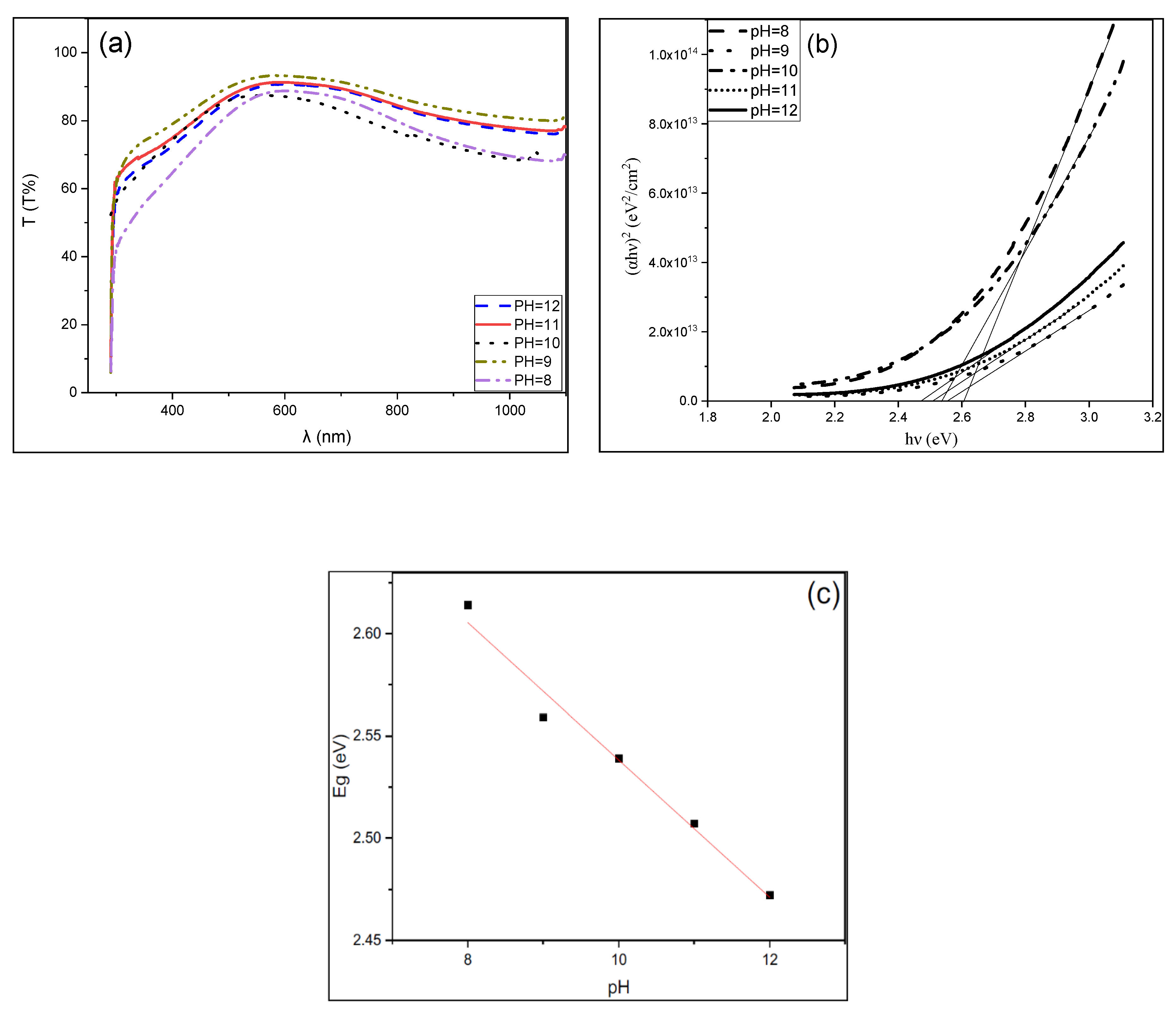
Optical transmittance using different pH levels is shown in Figure 22. The transmission line varies from 60% to 87% from the wavelength in the range 300 to 600 nm and shows a gradual decrease from 600 nm to 1100 nm, and it has the highest peak at the visible range of 600 nm for pH = 9. pH = 8 has a sharper transmittance increase from 40% to 84% in the range of 300 to 600 nm [28], and pH 12 and 11 are almost the same across the transmission line. The transmission line shows a blue shift with increasing pH.
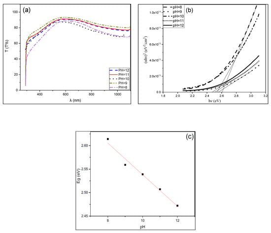
Figure 22.
(a) The effect of pH on the optical transmittance of CuS films at a deposition time 20 min. and temperature 80 °C. (b) Tauc plots of (αhν)2 against hν for different pH levels of the solution, and (c) the relationship between the energy gap and pH of the solution.
Figure 23 represents the effect of the pH rate on the optical energy gaps. A strong linear decrease of the energy gap with respect to pH rate is observed as in Figure 23 from 2.61 eV to 2.47 eV. This is related to the growth conditions; films grown at higher pH are thicker than the films made at low pH, and hence the band gap decreases. These results are confirmed by Reference [35].
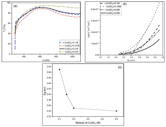
Figure 23.
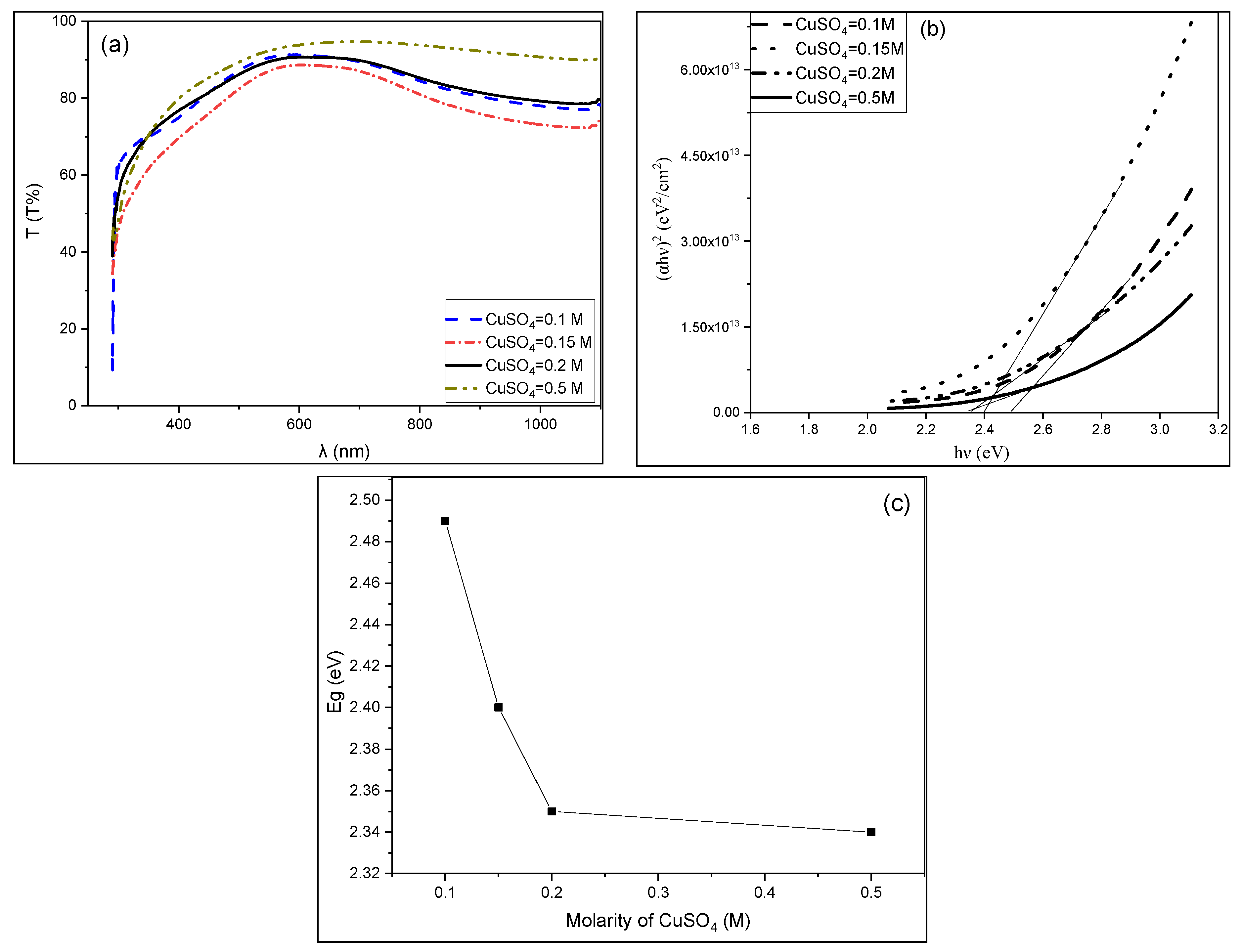
(a) The effect of the copper ion concentration on the optical transmittance of CuS films at a deposition time of 20 min, a temperature 80 °C, and pH = 11. (b) The relationship between (αhν)2 against hν of different CuSO4 concentrations, and (c) the relationship between the molarity of CuSO4 and the energy gap.
Optical transmittance using different copper concentrations is shown in Figure 23a. It can be seen that at the higher the concentration, the transmittance is higher [25]. While there is a slightly noticeable change in the IR region, these high values may be attributed to low band gaps due to the increased thickness of the films since thicker films have more atoms present so more states will be available for the photons to be absorbed [36,37], or due to quantum confinement effects [25,38]
At the visible region, all the concentrations showed the same behavior, and less than 5% transmittance is noticed.
Figure 23b,c shows the Tauc plot of the energy gap and the effect of copper concentration on the optical bandgap energy, respectively. A clear dependence of the energy gap on copper concentration is seen; as the concentration of CuSO4 increases, the band gap decreases [25]. The bandgaps obtained are 2.49, 2.4, 2.35, and 2.34 eV for 0.1 M, 0.15 M, 0.2 M and 0.5 M CuSO4 concentrations, respectively, and these values are in agreement with the values reported by others [25,27,39].
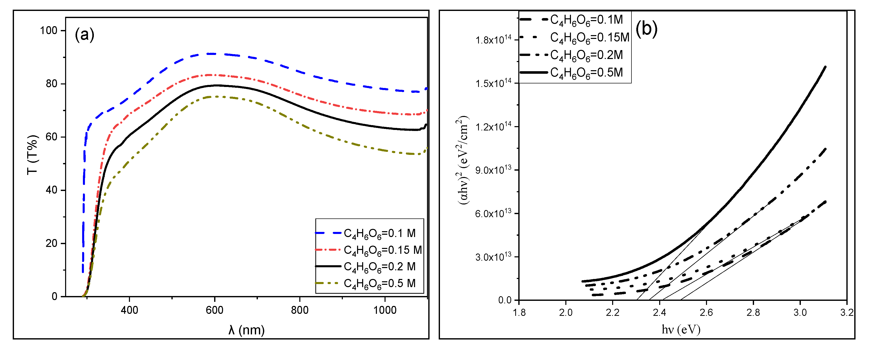
Clear regular change in the behavior of transmittance is observed in Figure 24a for different tartaric acid (C4H6O6) concentrations. It can be seen that at higher concentrations, the transmittance is lower throughout the whole range of wavelength because thickness increases with the increasing tartaric acid concentration.
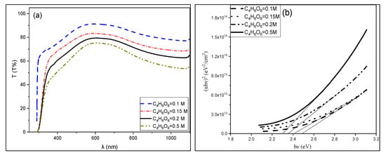
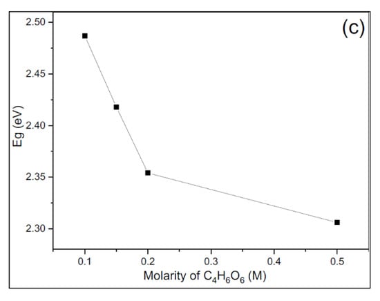
Figure 24.
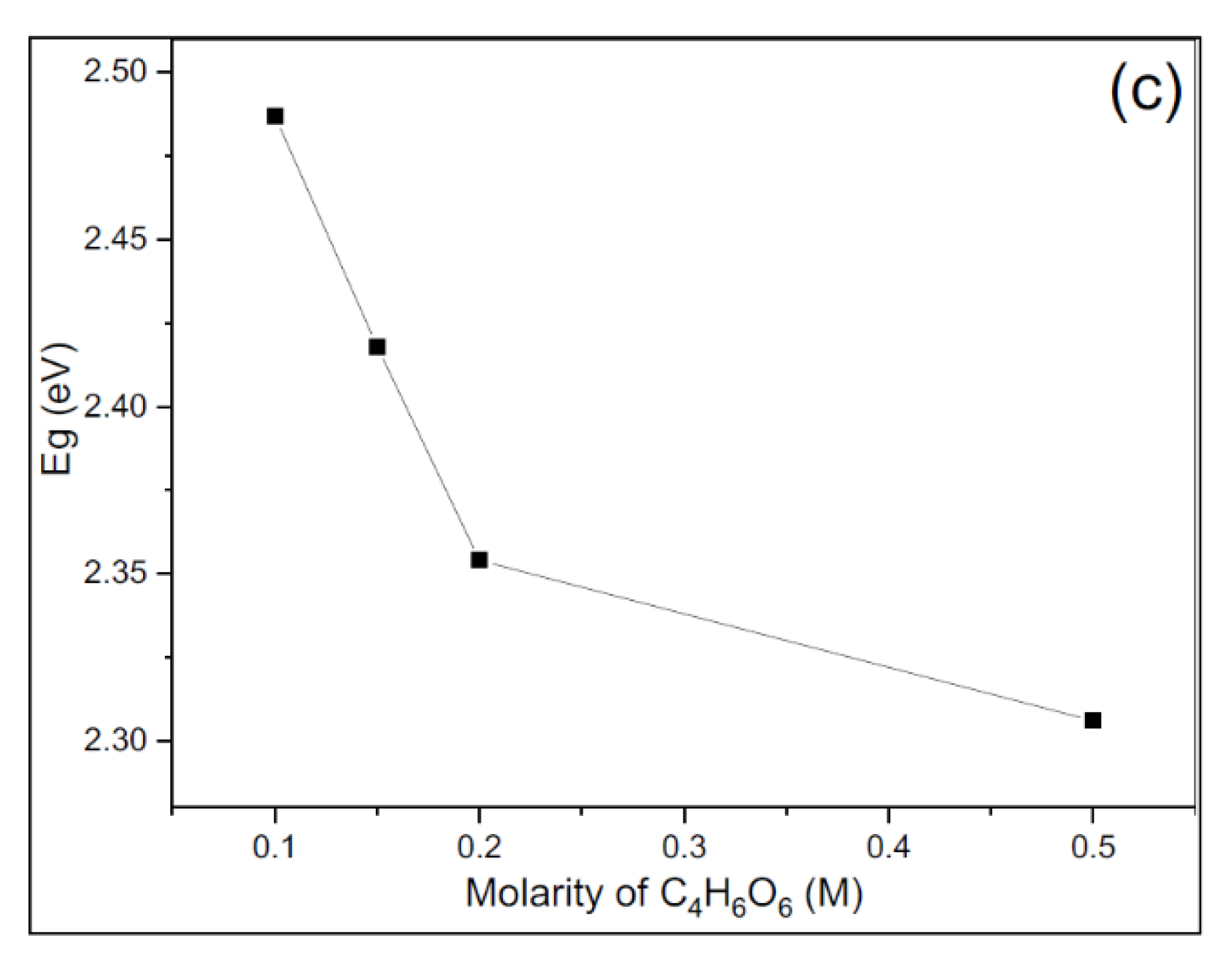
(a) The effect of C4H6O6 concentration on the optical transmittance of CuS films at a deposition of 20 min, a temperature of 80 °C, and pH = 11. (b) The relationship between (αhν)2 against hν of different C4H6O6 concentrations, and (c) the relationship between the molarity of C4H6O6 and the energy gap.
Figure 24b,c shows the Tauc’s relation of the energy gap with respect to the tartaric acid concentration and the effect of the concentration on the energy gap. The energy gap decreases with the increasing concentration of the tartaric acid.
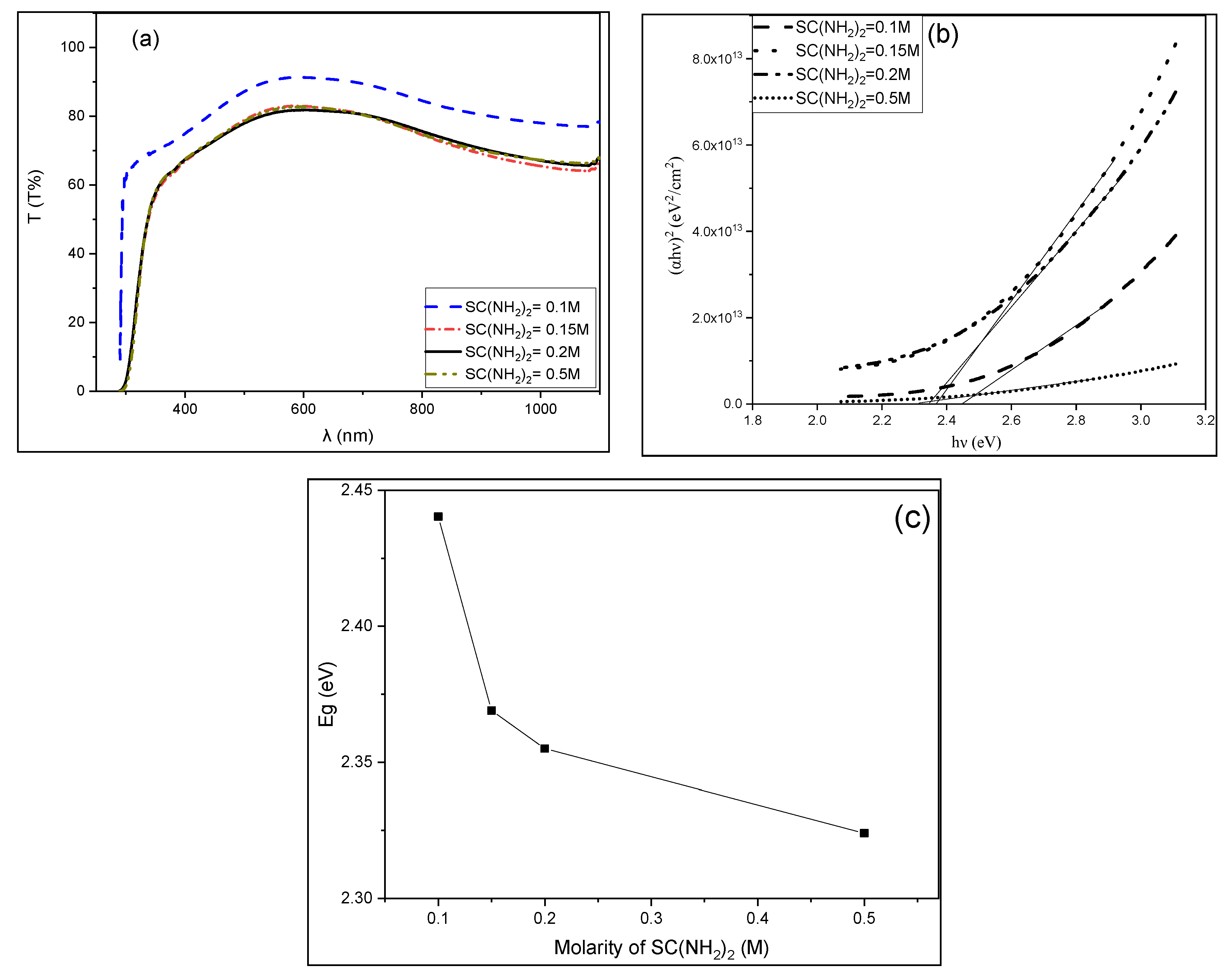
Figure 25 shows the influence of the SC(NH2)2 concentration on optical transmittance. No significant change is seen at higher concentrations of SC(NH2)2, but at 0.1 M the transmission showed the highest peak of 94%. Another point that can be noticed, which is that no shift in the transmission line is seen with the increasing SC(NH2)2 concentration.
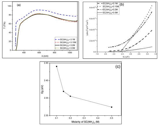
Figure 25.
(a) The effect of SC(NH2)2 concentration on the optical transmittance of CuS films at a deposition time of 20 min, a temperature of 80 °C, and pH = 11. (b) The relationship between (αhν)2 against hν of different SC(NH2)2 concentrations, and (c) the relationship between the molarity of SC(NH2)2 and the energy gap.
3.4. Electrical Properties of CuS Thin Films
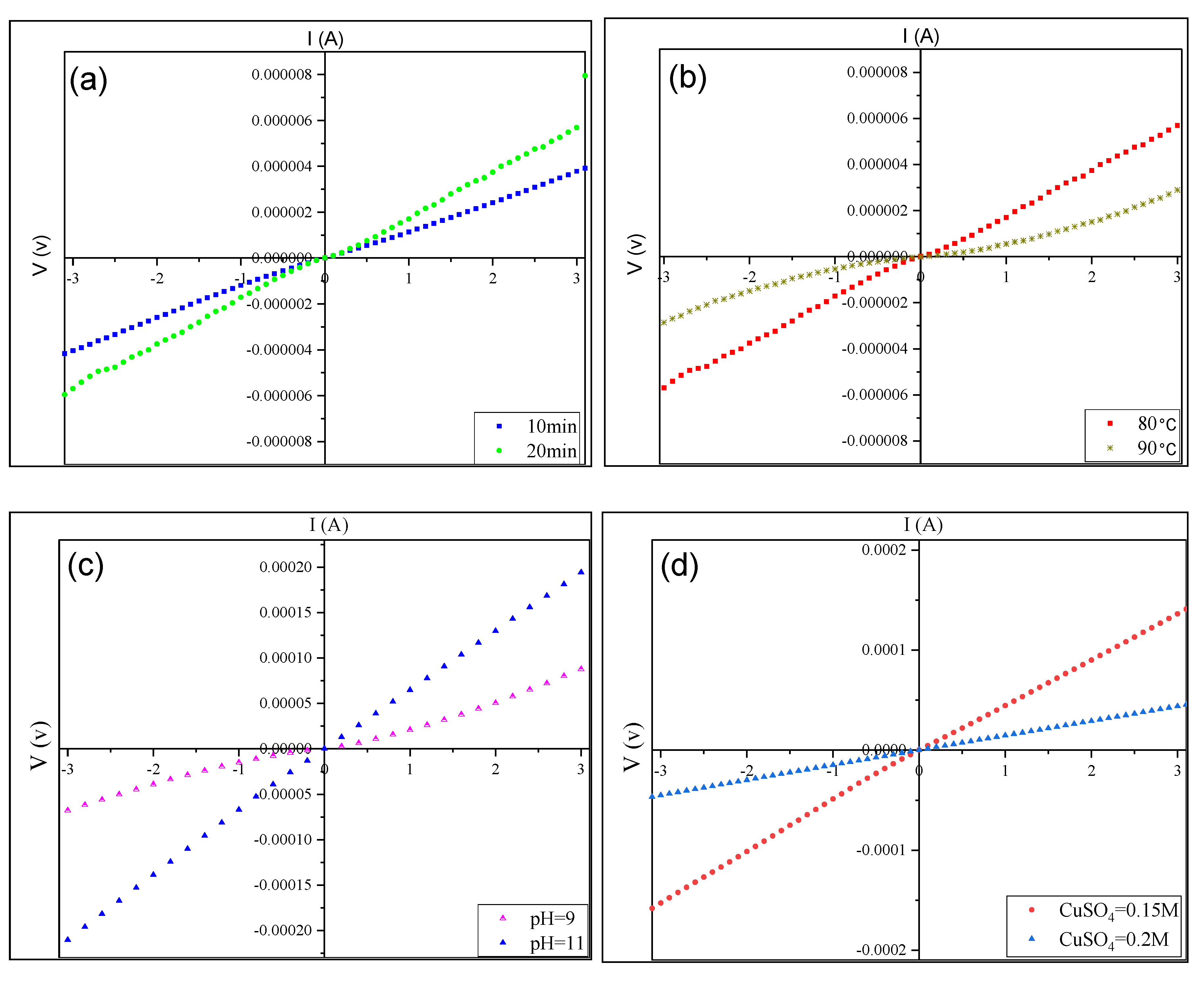
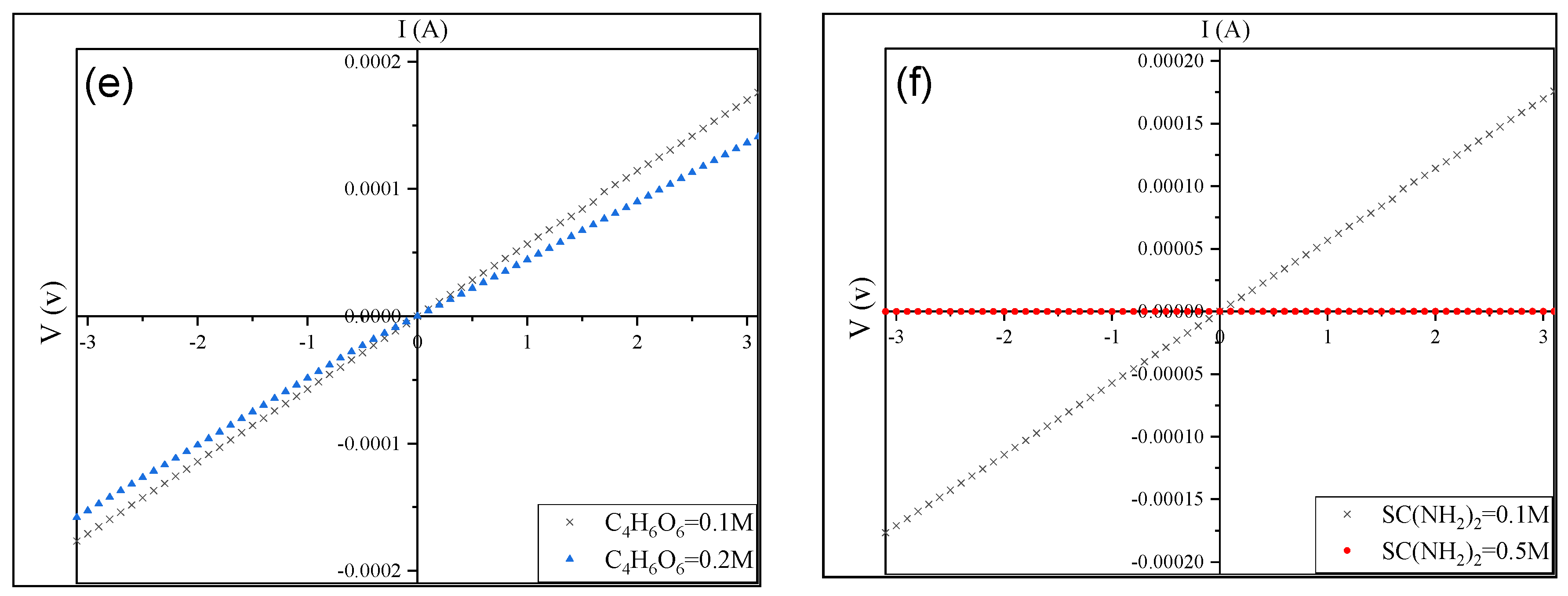
Figure 26 represents the current-voltage characteristics for CuS thin films fabricated at different deposition parameters. The electrical contacts are made from Aluminum (Al) [16].
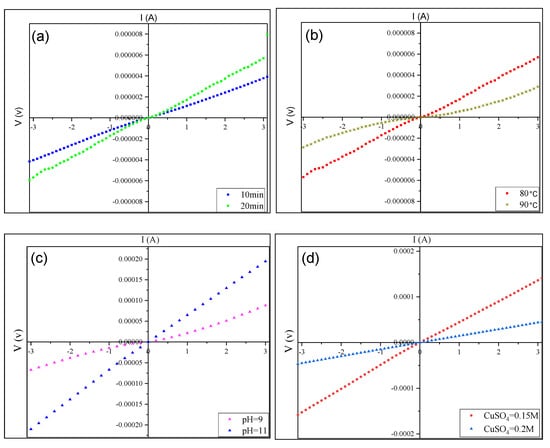

Figure 26.
I-V characteristic of the CuS thin film due to different (a) deposition times, (b) deposition temperatures, (c) pH of solution, (d) CuSO4 concentration, (e) SC(NH2)2 concentration, and (f) C4H6O6 concentration.
From the figures, it can be seen that the relationship of the current-voltage is linear. The forward and reverse bias linear relationship proves that there is an ohmic contact between Al-CuS.
Table 2 and Table 3 represent the effect of different deposition parameters on the electrical resistivity of the thin films. The resistivity in CuS films decreases as the deposition time increases. This decrease is due to thickness dependence [27,31,40]

Table 2.
The effect of the deposition temperature and deposition time on electrical resistivity.

Table 3.
The effect of different Precursor concentrations of CuSO4, SC(NH2)2, C4H6O6, and pH on electrical resistivity.
An increase in resistivity is obtained with increasing deposition temperatures, and that could be due to an increase in grain boundary barrier height [27,41]. For different pH levels of the solution, resistivity increases, as shown in Table 3. This is may be attributed to a deviation from stoichiometry due to the enhancement of the concentration of copper ions [27].
A large decrease in the resistivity is shown when increasing the concentration thiourea. As shown in Table 3, this large thiourea volume is induced by the creation of excess copper vacancies which give rise to a large number of free holes. Actually, as thiourea is the source for Sulphur, one can expect a larger concentration of copper vacancies [27].
Both the cases of increasing concentration of CuSO4 and tartaric acid lead to larger electrical resistivity from 0.7 to 2.41 Ω·cm for 0.15 and 0.2 M of CuSO4 concentration, and 0.78 to 1795.1 Ω·cm for 0.1 and 0.5 M of tartaric acid, respectively.
Table 4 and Table 5 represent the values of the electrical activation energy of different bath parameters. At a low time of deposition, the activation decreases with time, and the activation energy decreased from 0.012 eV to 0.009 eV. These results are in agreement with Reference [27]. For different pH levels of the solution, the activation energy decreases with increasing pH, as is shown in Table 5 [27]. Deposition temperature has a reverse relationship with the activation energy, and it has been decreased from 0.009 eV to 0.003 eV for deposition temperatures of 80 °C and 90 °C, respectively. The activation energy was in the range mentioned in References [41,42].

Table 4.
Electrical activation energy of CuS thin films due to different deposition times and deposition temperatures.

Table 5.
Electrical activation energy of CuS thin films due to different bath concentrations of CuSO4, SC(NH2)2, and C4H6O6, and pH.
4. Conclusions
CuS thin films were successfully deposited onto commercial glass according to various deposition parameters using chemical bath deposition. CBD is an easy, available, and cheap technology for controlling the structure, optical, and electrical properties of CuS thin films. It has been concluded that the thickness of the Cus thin film is affected by the concentration of the precursors. The use of 0.15 M of CuSO4 and thiourea gives a low thickness, and 0.1 M of tartaric acid gives a low thickness.
The structure of the obtained CuS thin films indicated that all the films show an amorphous structure except the case of the optimum conditions.
The transmittance of the CuS thin films tell us that the films absorb heavily in the UV and partly in the VIS regions but moderately in the near-IR regions.
The deposition time, deposition temperature, pH, and CuSO4 concentration have less of an effect on electrical resistivity. In contrast, the concentrations of C4H6O6 and SC(NH2)2 have a large influence on the resistivity. Activation energy decreases with increasing deposition temperature, deposition time, solution pH, CuSO4, and thiourea concentration, while it has a direct relationship with the increase of C4H6O6.
The optical characterization within the UV-VIS region shows that the growth CuS thin film has potential applications as absorbers for photovoltaic conversion in solar cells.
Author Contributions
Conceptualization, S.M.A. and R.Y.M.; methodology, S.M.A. and R.Y.M.; software, K.A.M.; validation, S.M.A., R.Y.M. and K.A.M.; formal analysis, S.M.A. and R.Y.M.; investigation, R.Y.M.; resources, R.Y.M.; data curation, K.A.M.; writing—original draft preparation, K.A.M.; writing—review and editing, S.M.A. and R.Y.M.; visualization, K.A.M.; supervision, S.M.A. and R.Y.M.; project administration, S.M.A. and R.Y.M.; funding acquisition, University of Duhok. All authors have read and agreed to the published version of the manuscript.
Funding
This research was funded by University of Duhok.
Acknowledgments
The acknowledgment is directed to Soran University and Koya University for their technical support.
Conflicts of Interest
First the authors declare no conflict of interest. Second the funders had no role in the design of the study; in the collection, analyses, or interpretation of data; in the writing of the manuscript, or in the decision to publish the results.
References
- Shen, Y.; Xu, N.; Hu, W.; Xu, X.; Sun, J.; Ying, Z.; Wu, J. Bismuth doped ZnSe Films fabricated on selecone substrate by pulsed laser deposition. Solid State Electron. 2008, 52, 1833–1836. [Google Scholar] [CrossRef]
- Thanikaikarasan, S.; Mahalingam, T.; Adaikalam, K. Characterization of electrodeposited Copper Sulphide thin fil. New Mater. Electrochem. Syst. 2009, 13, 29–33. [Google Scholar]
- Aperathitis, E.; Bryant, F.; Scott, C. Evaporated Copper Sulphide Layers for All-Vacuum Evaporated CuxS/CdS Solar Cell; Elsevier: Amsterdam, The Netherlands, 1990; Volume 20, pp. 15–28. [Google Scholar]
- Chisomam, U.; Charity, O.; Israel, O. Analysis of Chemically deposited Copper Sulfide thin film. Chmeistry Mater. Res. 2014, 6, 1–8. [Google Scholar]
- Luminita, I.; Anca, D.; Angela, K.; Simona, M.; Marian, N. Copper Sulfides obtained by Spray Pyrolysis-Possible absorbers in solid state solar cell. Thin Solid Film. 2007, 515, 5755–5758. [Google Scholar]
- Guizeldir, B.; Saglam, M.; Ates, A. Deposition and characterization of CdS, CuS and ZnS thin films deposition by SILAR Metho. In Proceedings of the Internaional Congress and Advanced in Applied Physics and Material Science, Antalya, Turkey, 12–15 May 2011; Volume 2, pp. 33–35. [Google Scholar]
- Ahamed, M.; Basheer, S.; Bale, A.; Nagarethiam, V.; Thayumanavan, A.; Sanjeeveraja, C.; Jayachandran, M. Structural, optical and electrical properities of electron beam evaporated CdSe thin film. Cryst. Res. Technol. 2010, 45, 387–392. [Google Scholar] [CrossRef]
- Ghribi, F.; Alyamani, A.; Ben Ayadi, Z.; Djessas, K.; EL Mir, L. Study of CuS Thin Films for Solar Cell Applications Sputtered from Nanoparticles Synthesised by Hydrothermal Rout; Elsevier Ltd.: Amsterdam, The Netherlands, 2015; Volume 84, pp. 197–203. [Google Scholar]
- Goel, S.; Chen, F.; Cai, W. Synthesis of Biomedical Applications of Copper Sulfide Nanoparticles, from Sensors to Theranostic; Wiley Online Library: Hoboken, NJ, USA, 2014; Volume 10, pp. 31–45. [Google Scholar]
- Basu, M.; Sinha, A.K.; Pradhan, M.; Sarkar, S.; Negishi, Y.; Govind, T. Evolution of Hierarchial Hexagonal Stacked plates of CuS from liquid-liquid interface and its Photocatalytic Application for Oxidative Degradation of Different Dyes under Indoor Lightin. ACS Publ. 2010, 6, 6313–6318. [Google Scholar]
- Tian, X.; Qian, L.; Mao, J.; Yuan, H. In Situ Synthesis of CuS nanotubes on Cu electrode for Sensitive nonenzymatic Glucose Senso. Sens. Actuators B Chem. 2013, 176, 952–959. [Google Scholar]
- Chung, J.; Sohn, H. Electrochemical behavior of CuS as a CCathode material for lithium Secondery Batterie. Power Sour. 2002, 108, 226–231. [Google Scholar] [CrossRef]
- Shamraiz, U.; Azadar, R.; Badshah, A. Fabrication and applications of copper sulfide (CuS) nanostructure. J. Solid State Chem. 2016, 238, 25–40. [Google Scholar] [CrossRef]
- McPeak, K.M. Chemical Bath Deposition of Semiconductor Thin Films & Nanostructures in Novel Microreactors. Ph.D. Thesis, Drexel University, Drexel, PA, USA, 2010. [Google Scholar]
- Singh, A.; Mehra, S.; Thool, G. Synthesis of copper Sulfide (CuS) thin film by chemical bath deposition method and its chracterizatio. Eur. Chem. Bull. 2013, 2, 518–523. [Google Scholar]
- Schwartz, B. Ohmic Contacts to Semiconductors; The Electrochemical Society: Pennington, NY, USA, 1969. [Google Scholar]
- Chopra, K.L. Thin Film Phenomena; Mcgraw-Hill Book Company: Boston, MA, USA, 1979. [Google Scholar]
- Elttayaf, A.-H.K.; Ajeel, A.E. Kudair, preparation and study the structural and optical properities of CuS nano fil. Int. J. Thin Films Sci. Technol. 2013, 2, 223–231. [Google Scholar] [CrossRef][Green Version]
- Maria, P.; Gutiérrez, H.L.; Patton, J. Thin Film Surface Resistivity. Available online: http://citeseerx.ist.psu.edu/viewdoc/download?doi=10.1.1.528.6542&rep=rep1&type=pdf (accessed on 6 August 2020).
- Mott, N.; Davis, E. Electronic Processes in Non-Crystalline Materials; Clarendon Press: Oxford, UK, 1987. [Google Scholar]
- Zeyada, H.; El-Nahass, M.; Makhlouf, M. Electronic transport mechanisms in tetraphenyleprophyrin thin film. Curr. Appl. Phys. 2011, 11, 1326–1331. [Google Scholar] [CrossRef]
- Sudha, L.K.; Sukumar, R. Evaluation of Activation Energy (Ea) Profiles of Nanostructured Alumina Polycarbonate Composite Insulation Material. Int. J. Mater. Mech. Manuf. 2014, 2, 96–100. [Google Scholar]
- Munce, C.G. Chemical Bath Deposition of Copper Sulfide Thin Films. Ph.D. Thesis, Griffith University, Queensland, Austraila, July 2008. [Google Scholar]
- Vas-Umnuay, P.; Chih-hung, C. Growth Kinetics of Copper Sulfide Thin Films by Chemical Bath Depositio. ECS J. Solid State Sci. Technol. 2013, 2, 120–129. [Google Scholar] [CrossRef]
- Sangamesha, M.; Pushapalatha, K.; Shekar, G. Effect of concentration on structural and optical properties of CuS thin film. Int. J. Res. Eng. Technol. 2013, 2, 227–234. [Google Scholar]
- Thornton, J.A. The microstructure of sputter-deposited coating. J. Vac. Sci. Technol. 1988, 4, 3059. [Google Scholar] [CrossRef]
- Ali, M.; Samir, H.; Jean, P. Influence of depositionparameters on optical andelectrical properties of CuxS thin films prepared using chemical bath deposition metho. Iraqi J. Appl. Phys. 2008, 4, 1813–2065. [Google Scholar]
- Ilenikhena, P.K. Comparitive Studies of Improved Chemical Bath Deposited Copper Sulphide (CuS) and Zinc Sulphide (ZnS) Thin Films at 320K and Possible Applications. Afr. Phys. Rev. 2008, 2, 59–67. [Google Scholar]
- Kassim, A.; Nagalingam, S.; Tee, T.W.; Koon, K.L. Effect of PH value and electrolyte concentration on the Copper Sulfide thin films prepared by chemical bath deposition method. GUJS 2010, 23, 435–443. [Google Scholar]
- Al-Khayatt, A.H.O.; Jaafer, M.D. Annealing Effect on The Structuraland Optical Properties of CuS Thin Film Prepared by Chemical Bath Deposition (CBD). J. Kufa Phys. 2013, 5, 79–90. [Google Scholar]
- Carrillo Castillo, A.; Ambrosio Lazaro, R.; Lira Ojeda, E.; De la mota Gonzalez, M.; Quevedo Lopez, M.; Moreno Moreno, M.; Gonzalez Diaz, V.; Guerrero Castellanos, J. charactirization of amourphous CuS thin films obtained from fast time and low temperature of deposition. Chalcogenide Lett. 2016, 13, 217–224. [Google Scholar]
- Nemade, K.; Waghuley, S. Band gap engineering of CuS nanoparticles for artificial photosynthesis. Elsevier Mater. Sci. Semicond. Process. 2015, 39, 781–785. [Google Scholar] [CrossRef]
- Ezima, F.; Nnabuchi, M.; Osuji, R. Optical properities of CuS thin films deposited by chemical bath deposition technique and their applications. Trends Appl. Sci. Res. 2006, 1, 467–476. [Google Scholar]
- Min, H.S.; Kassim, A.T.; Weetee, T.; Nagalingham, S. The Effect of Bath Temperature on the Chemical Bath Deposition of Copper Sulphide Thin Films. Jordan J. Chem. 2010, 5, 165–173. [Google Scholar]
- Mamiyev, Z.Q.; Balayeva, N.O. CuS Nanoparticles Synthesized by a Facile Chemical Route Under Different pH Conditions; Elsevier: Amsterdam, The Netherlands, 2016; Volume 26, pp. 235–237. [Google Scholar]
- Ali, M.; Abbas, F. Influence of post-annealing on the properties of CuxS:Al, Fe films deposited by CBD. J. Eng. Technol. 2009, 27, 1112–1150. [Google Scholar]
- Ngahu, K.M. Optical and Electrical Analysis of Cd1-XFeXS/CuS P-N Junction for Solar Cell Application. Master’s Thesis, School of Pure and Applied Sciences of Kenyatta University, Nairobi City, Kenya, November 2016. [Google Scholar]
- Reda, S.; El-Sherbieny, S. Dye-sensitized nanocrystalline CdS and ZnS solar cells with different organic dyes. J. Mater. Res. 2010, 25, 522–528. [Google Scholar] [CrossRef]
- Popovici, I.; Isac, A. Electrical Conductivity Incopper Sulfides—Influence of Thedeposition Parameters Andprecursor’s Concentration; Bulletin of the Transilvania University: Brasov, Romania, 2009; Volume 2. [Google Scholar]
- Shinde, M.; Ahirrao, P.; Patil, I.; Patil, R. Thickness dependent electrical and optical properties of nanocrystalline copper Sulphide thin films grown by simple chemical route. Indian J. Pure Appl. Phys. 2012, 50, 657–660. [Google Scholar]
- Sabah, F.A.; Ahmed, N.M.; Hassan, Z.; Rasheed, H.S. Effect of Annealing on the Electrical Properties of CuxS Thin Films. Procedia Chem. Elsevier 2016, 19, 15–20. [Google Scholar] [CrossRef]
- Santos, J.; Cruz, S.; Mayeb Hernandez, F.; Paraguay Delgado, O.; Zelaya Angel, R.; Castanedo, P.; Torres Delgado, G. Optical and Electrical Properties of Thin Films of CuS Nanodisks Ensembles Annealed in a Vacuum and Their Photocatalytic Activity. Int. J. Photoenergy 2013, 4, 1–9. [Google Scholar] [CrossRef]
© 2020 by the authors. Licensee MDPI, Basel, Switzerland. This article is an open access article distributed under the terms and conditions of the Creative Commons Attribution (CC BY) license (http://creativecommons.org/licenses/by/4.0/).


