Article

GaN-Based LEDs Grown on Graphene-Covered SiO2/Si (100) Substrate

1
Research and Development Center for Solid State Lighting, Institute of Semiconductors, Chinese Academy of Sciences, Beijing 100083, China
2
Center of Materials Science and Optoelectronics Engineering, University of Chinese Academy of Sciences, Beijing 100049, China
3
Anhui Province Engineering Laboratory for Antennas and Microwave Hefei, Hefei 230088, China
4
School of Materials and Energy, University of Electronic Science and Technology of China, Chengdu 610054, China
*
Authors to whom correspondence should be addressed.
Crystals 2020, 10(9), 787; https://doi.org/10.3390/cryst10090787
Submission received: 5 August 2020 / Revised: 30 August 2020 / Accepted: 4 September 2020 / Published: 5 September 2020
(This article belongs to the Special Issue Nitride Compound Light Emitting Diodes)

Abstract

:
The growth of nitride on large-size and low-cost amorphous substrates has attracted considerable attention for applications in large-scale optoelectronic devices. In this paper, we reported the growth of GaN-based light-emitting diodes (LEDs) on amorphous SiO2 substrate with the use of nanorods and graphene buffer layers by metal organic chemical vapor deposition (MOCVD). The effect of different growth parameters on the morphology and vertical-to-lateral aspect ratio of nanorods was discussed by analyzing growth kinetics. Furthermore, we tuned nanorod coalescence to obtain continuous GaN films with a blue-LED structure by adjusting growth conditions. The GaN films exhibited a hexagonal wurtzite structure and aligned c-axis orientation demonstrated by X-ray diffractometer (XRD), Raman, and transmission electron microscopy (TEM) results. Finally, five-pair InGaN/GaN multi-quantum-wells (MQWs) were grown. The photoluminescence (PL) showed an intense emission peak at 475 nm, and the current–voltage (I-V) curve shows a rectifying behavior with a turn-on voltage of 5.7 V. This work provides a promising fabrication method for the large-area and low-cost GaN-based devices on amorphous substrates and opens up the further possibility of nitride integration with Si (100) complementary metal oxide semiconductor (CMOS) electronics.

Graphical Abstract

1. Introduction

In recent years, GaN-based semiconductor materials have attracted considerable attention as significant building blocks for widespread applications on optoelectronic devices, such as light-emitting diodes (LEDs), laser diodes (LDs), as well as high-frequency and high-power transistors owing to their outstanding optical and electrical performance [1,2,3]. Conventionally, for a very long time, most GaN-based epitaxial layers have been grown on single-crystalline substrates such as sapphire, Si (111), and 6H-SiC by metal organic chemical vapor deposition (MOCVD) or molecular beam epitaxy (MBE) [4,5,6,7]. However, on account of the high cost and small size of the single-crystal substrates, GaN-based LEDs may be restricted for future applications in large-sized, flat, inexpensive light sources such as back-light units for liquid crystal display televisions [8]. Therefore, it is necessary to grow GaN-based devices on substrates with low fabrication costs and large areas, such as amorphous SiO2 substrates. However, these conventional epitaxy methods are no longer suitable due to the lack of epitaxial growth relationship between the amorphous substrate with nitrides, making it challenging to directly grow nitride materials on the amorphous substrate.
Ideally, graphene as a dangling-bond-free two-dimensional planar material can prevent the propagation of crystalline information from the underlying substrates by introducing the different bonding mechanisms in van der Waals epitaxy (vdWE) [9,10], in which the grown epilayers need not be necessarily lattice-matched with the underlying substrate [11]. Hence, graphene acting as a buffer layer has attracted much interest in recent years, such as GaN-based LEDs prepared on graphene-covered sapphire [12,13,14], vertical-layout AlGaN nanorods obtained on graphene/silicon [15,16,17], and high-quality GaN or AlN films grown on graphene/SiC [18,19,20]. However, these works are all based on single crystalline substrates. Meanwhile, due to the absence of dangling bonds, the pristine graphene surface causes high surface tension, leading to weak nucleation and cluster growth for the GaN buffer, which results in a high density of defects such as stacking faults and threading dislocations during the coalescence of nitrides [21,22]. In this aspect, our group has previously proved the feasibility of AlGaN nanowire grown on the SiO2/Si (100) substrate assisted with graphene [23]. Here, we further grow GaN films with the use of AlGaN nanorods and graphene buffer layers on the amorphous substrate.
In this work, AlGaN nanorods were directly grown on single-layer graphene covered SiO2/Si (100) substrates, and we adopted the method of controlled nanorods coalescence to obtain continuous GaN films by MOCVD. Firstly, we studied the growth behaviors of AlGaN nanorods by tuning the reactor pressure, NH3 flow, and growth temperature and obtained vertically aligned nanorods. Furthermore, continuous and flat GaN films were realized by adjusting the growth conditions of nanorods to the coalescence process. SEM, XRD, Raman, and TEM were used to characterize the morphology, quality, and crystal structure of GaN films. Finally, a blue-LED structure was grown on an amorphous SiO2 substrate. The multi-quantum-wells (MQWs) structure and optical properties of as-grown LEDs were analyzed by TEM, photoluminescence (PL) and the current–voltage (I-V) curves. This work represents a new attempt to solve the problem of growing nitride on the amorphous substrate, and it may be expected to realize the nitride integration with Si (100) complementary metal oxide semiconductor (CMOS) electronics in the future.

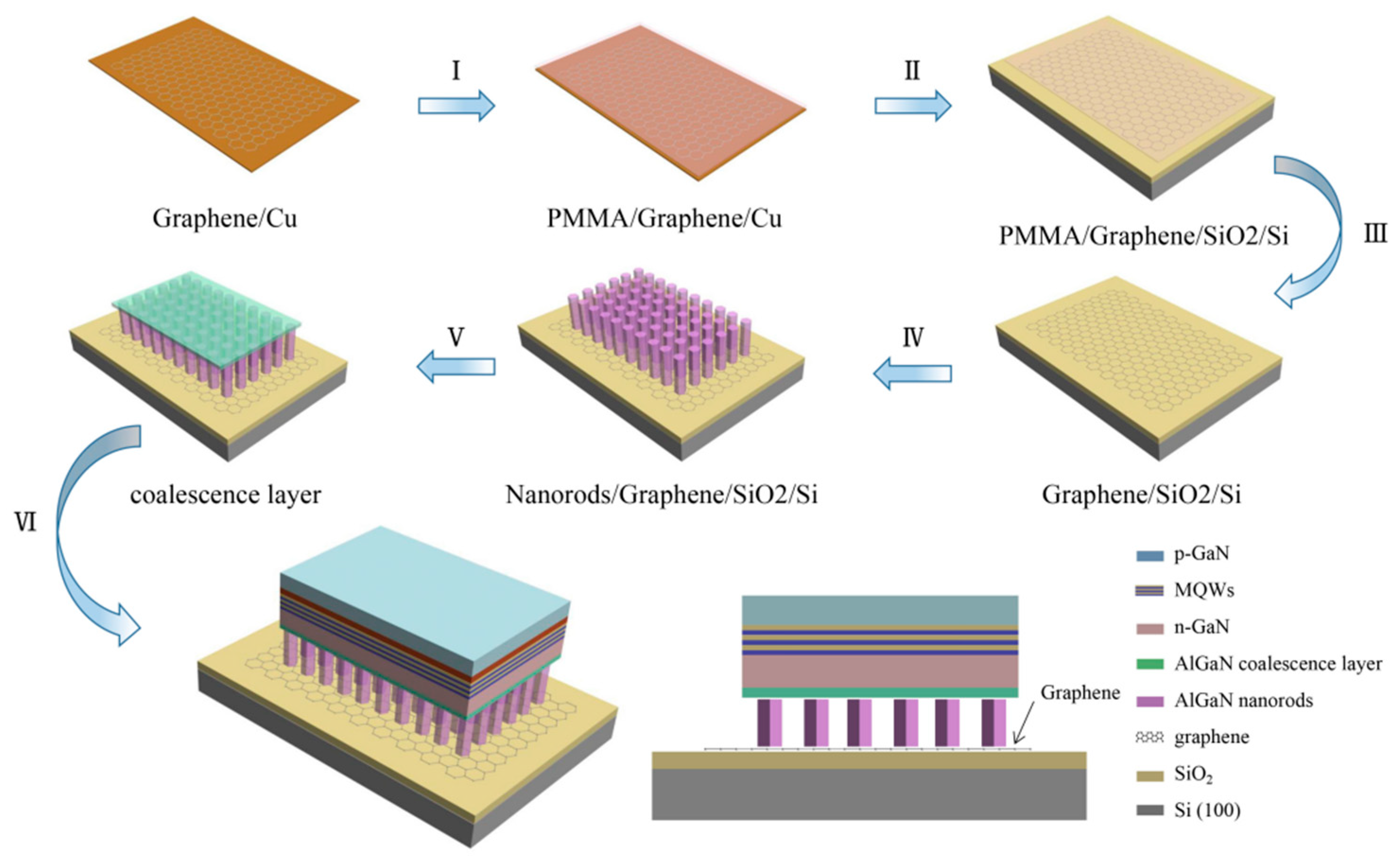
2. Materials and Methods

A schematic diagram including the graphene wet-transfer procedure and the growth of GaN films with the blue-LED structure on graphene-coated amorphous SiO2 (300 nm)/Si substrates utilizing nanorods coalescence is presented in Figure 1. Prior to the buffer layer growth, the process consisted of the following steps. First, the uniform monolayer graphene was synthesized on Cu foil by atmospheric-pressure chemical vapor deposition (APCVD, Xicheng, Xiamen, China), as reported previously [24]. After the growth, graphene was spin-coated with a protective layer of poly(methyl methacrylate) (PMMA) on the copper foil at 4000 rpm and baked on a hot plate at 120 °C for 15 min, which kept the graphene continuous in the next etching of the copper using aqueous solution of iron trichloride (FeCl3) for 4 h. After rinsing by deionized water three to four times, the released PMMA/graphene membrane could be transferred onto the target substrates. Subsequently, we acquired high-quality PMMA/graphene–SiO2 (300 nm)/Si substrates via scooping up and natural drying. Finally, the sample was soaked in an organic solvent with acetone and ethanol to remove the PMMA, leaving only monolayer graphene on the cleaned target substrate.
The LED structure consisted of an AlGaN nanorods/graphene buffer layer, a GaN coalescence layer, an Si-doped n-GaN layer, five pairs of InxGa1−xN/GaN multi-quantum-wells (MQWs), and an Mg-doped p-type GaN layer, as shown in Figure 1. All the temperatures at which we grew the material were the equipment-setting temperatures. Before the growth of nucleation, a nitridation process was carried out by introducing NH3 with a flow of 7200 sccm at 1280 °C for 150 s. It should be noted that GaN film directly grown on graphene was unsatisfactory, and AlGaN nucleation islands were thereby introduced due to the higher adsorption energy of an Al atom on graphene than a Ga atom. The nucleation islands were carried out at 1280 °C for 60 s under a growth pressure of 60 Torr. Then, an annealing process was carried out at 1280 °C for 60 s. To optimize the morphology of nanorods for the subsequent coalescence process, we designed a series of experiments to study the growth behaviors of AlGaN nanorods by manipulating the reactor pressure, NH3 flow, and temperature, which are summarized in Table 1. After the growth of good morphological nanorods buffer layer, the reactor pressure, NH3 flow, and growth temperature were changed to 120 Torr, 180 sccm, and 1240 °C respectively for 120 s to promote the lateral overgrowth to obtain a fully coalesced film. Then, the n-GaN layer was grown at the same growth conditions for 25 min with the silicane flow of 2.7 sccm. Furthermore, five pairs of GaN barriers and InxGa1-xN wells were grown at 940 °C and 850 °C, respectively. Finally, the Mg-doped p-GaN layer was further grown at 930 °C.
We used the MOCVD device (AIXTRON, a close-coupled showerhead system) to grow the material. The surface morphologies of the AlGaN nanorods and GaN films were observed using scanning electron microscopy (SEM, Hitachi, Tokyo, Japan) operated at 3 keV acceleration voltage, and the slanting angle between the sample and the electron beam was 25°. The microstructures of the sample were investigated by TEM (Tecnai, F20, Hillsboro, OR, USA). The X-ray diffraction pattern of the GaN films was measured by XRD (Bede D1, Durham, UK). The Raman spectroscopy of the GaN films was characterized by the measurement of Raman spectrometer (Horiba, Kyoto, Japan). Finally, to obtain the optical properties of the GaN-based LEDs, we analyzed the PL spectrum and the I-V curve.

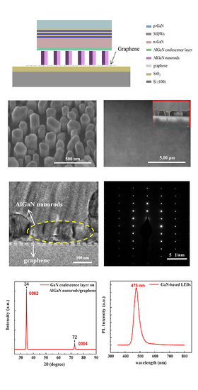
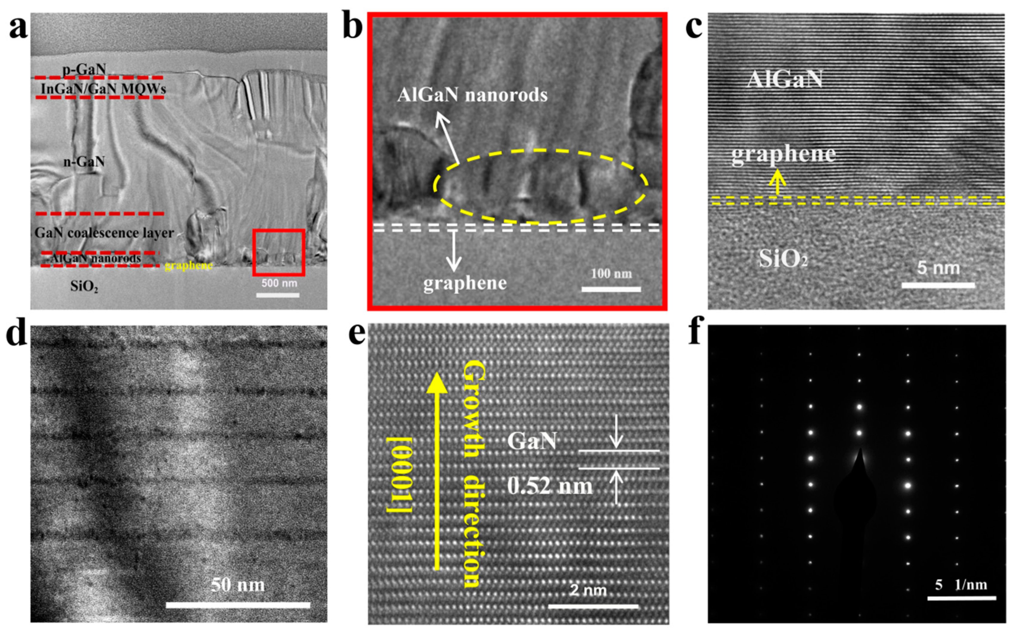
3. Results and Discussion

3.1. Effect of Reactor Pressure on AlGaN Nanorods

To study the effect of reactor pressure on the morphology of AlGaN nanorods grown on amorphous SiO2 (300 nm)/Si substrates with the graphene buffer layer, the pressure was varied from 120 Torr to 60 Torr, while the growth temperature and NH3 flow rate were maintained at 1280 °C and 90 sccm in the experiment set A, respectively.
Figure 2a–c show the 25° tilted-view scanning electron microscopy (SEM) images of the as-grown AlGaN nanorods with the growth reactor pressure of (a) 120 Torr, (b) 90 Torr, and (c) 60 Torr. It was obvious that the morphology of nanocrystals changed from nanopyramids to nanorods with decreasing the pressure. As shown in Figure 2a, the hexagonal pyramid grains were observed with an average diameter of approximately 103 nm under a reactor pressure of 120 Torr. When pressure decreased to 90 Torr (Figure 2b), nanopyramids exhibited a larger average diameter of approximately 126 nm. This might be due to the reducing pressure was beneficial to reinforce the migration rate of Ga and Al atoms, consequently promoting the formation of larger nanopyramids [23]. When the growth reactor pressure reached 60 Torr (Figure 2c), we obtained AlGaN nanorods with hexagonal symmetry along the c-axis direction [25]. Meanwhile, the {1–101} semipolar planes disappeared under the lower pressure, indicating that the growth rate of the {1–101} planes was relatively high. This should be attributed to the lower pressure leading to a reduction in the decomposition rate of ammonia, which reduced the effective V/III ratio and increased the mean free path of group III adatoms [23].
As previously reported, the growth of the {1–101} planes were related to a hydrogen-passivation effect. With a reduced concentration of hydrogen that decomposed from the NH3, the hydrogen-passivation effect was lessened, leading to faster growth of the {1–101} planes [26]. Moreover, Figure 2d–f present the histograms of the AlGaN nanorods’ profile distribution at different NH3 flow rates. It was obvious that there was a higher vertical-to-lateral aspect ratio of AlGaN nanorods in lower growth reactor pressure, which indicated that lower growth reactor pressure would promote the mobility of metal atoms. This growth rule could be more clearly reflected in Figure 2g, in which the vertical-to-lateral aspect ratio was inversely proportional to the pressure within a certain scope.

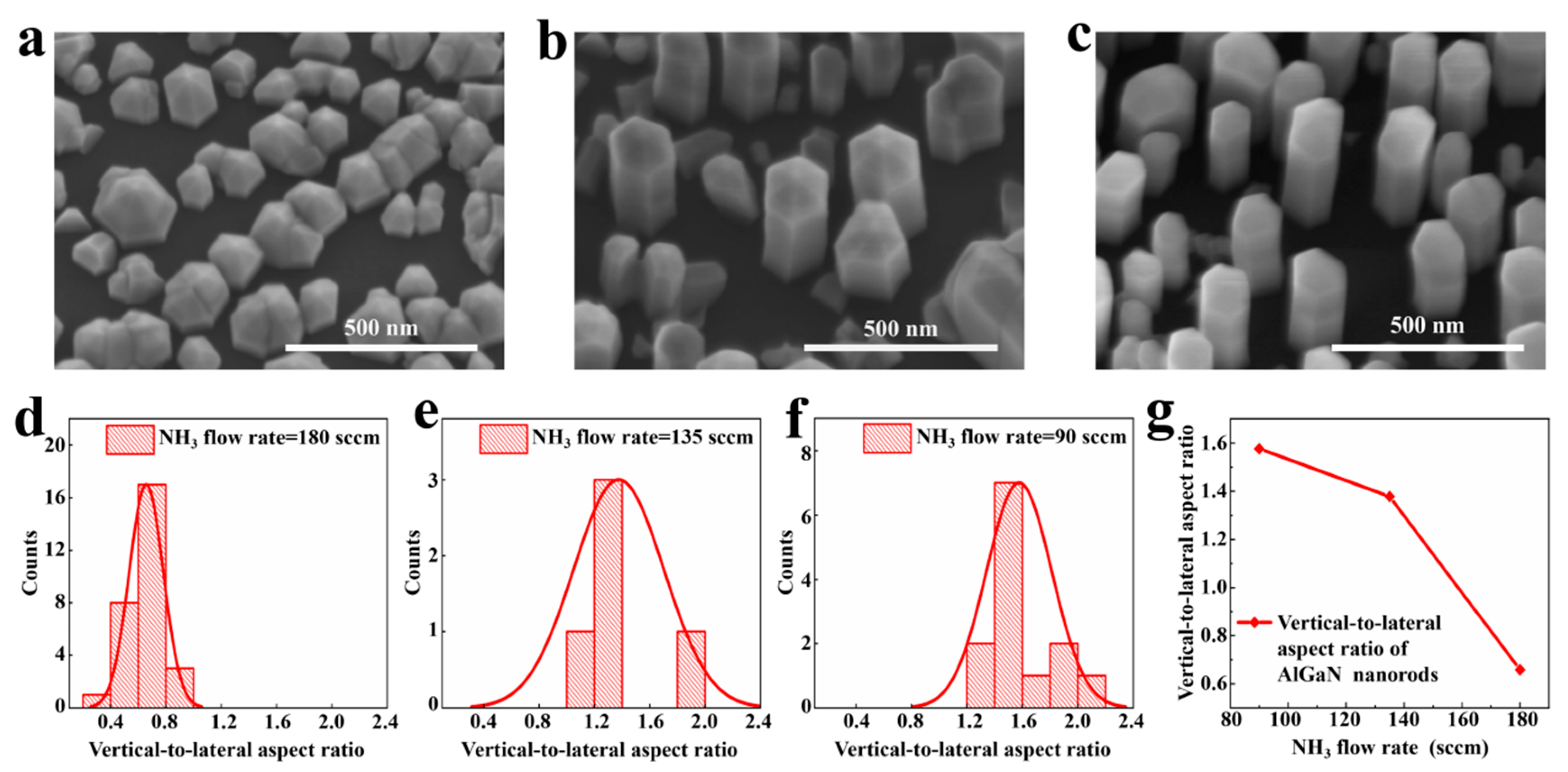
3.2. Effect of NH3 Flow Rate on AlGaN Nanorods

To further investigate the effect of the NH3 flow rate on the morphology of the as-grown AlGaN nanorods, we changed the NH3 flow rate from 180 to 90 sccm, while the reactor pressure and temperature were maintained at 60 Torr and 1280 ℃, as indicated in experiment set B.
Figure 3a–c show the SEM images (25° tilted-view) of the as-grown AlGaN nanorods with the NH3 flow rate of (a) 180 sccm, (b) 135 sccm, and (c) 90 sccm, accordingly. It could be seen that the large pyramidal-shaped AlGaN nanostructures with an average height and diameter about of 67 nm and 107 nm were dominant over the entire substrate when the NH3 flow rate was 180 sccm (Figure 3a). These nanopyramids clearly exhibited the formation of {1–101} sidewalls, indicating that the hydrogen atom decomposed from NH3 bonded with the nitrogen atoms on the semi-polar plane due to the hydrogen-passivation effect, which suppressed the growth rate along the {1–101} direction [27]. As the NH3 flow rate decreased to 135 sccm (Figure 3b), AlGaN nanorods were distributed on the substrate, but they still had pyramid-like structures at the top, demonstrating that the growth rate of the {1–101} planes was increased. When the NH3 flow rate declined from 135 to 90 sccm (Figure 3c), the top morphology of AlGaN nanorods changed from pyramid shape to a flat-topped columnar structure, indicating that the growth rate of the {1–101} plane was even faster than that of (0001).
In addition, the histograms and corresponding vertical-to-lateral aspect ratio distribution images of the AlGaN nanorods can be shown from Figure 3d–g. With a decrease in the NH3 flow rate, the vertical-to-lateral aspect ratio became higher. It inferred that a lower NH3 flow rate might lead to an insufficient supply of N atoms on the sidewall (m-plane) and a longer diffusion length of Ga adatoms to the c-plane under Ga-rich condition, which drastically promoted the longitudinal growth rate [28].

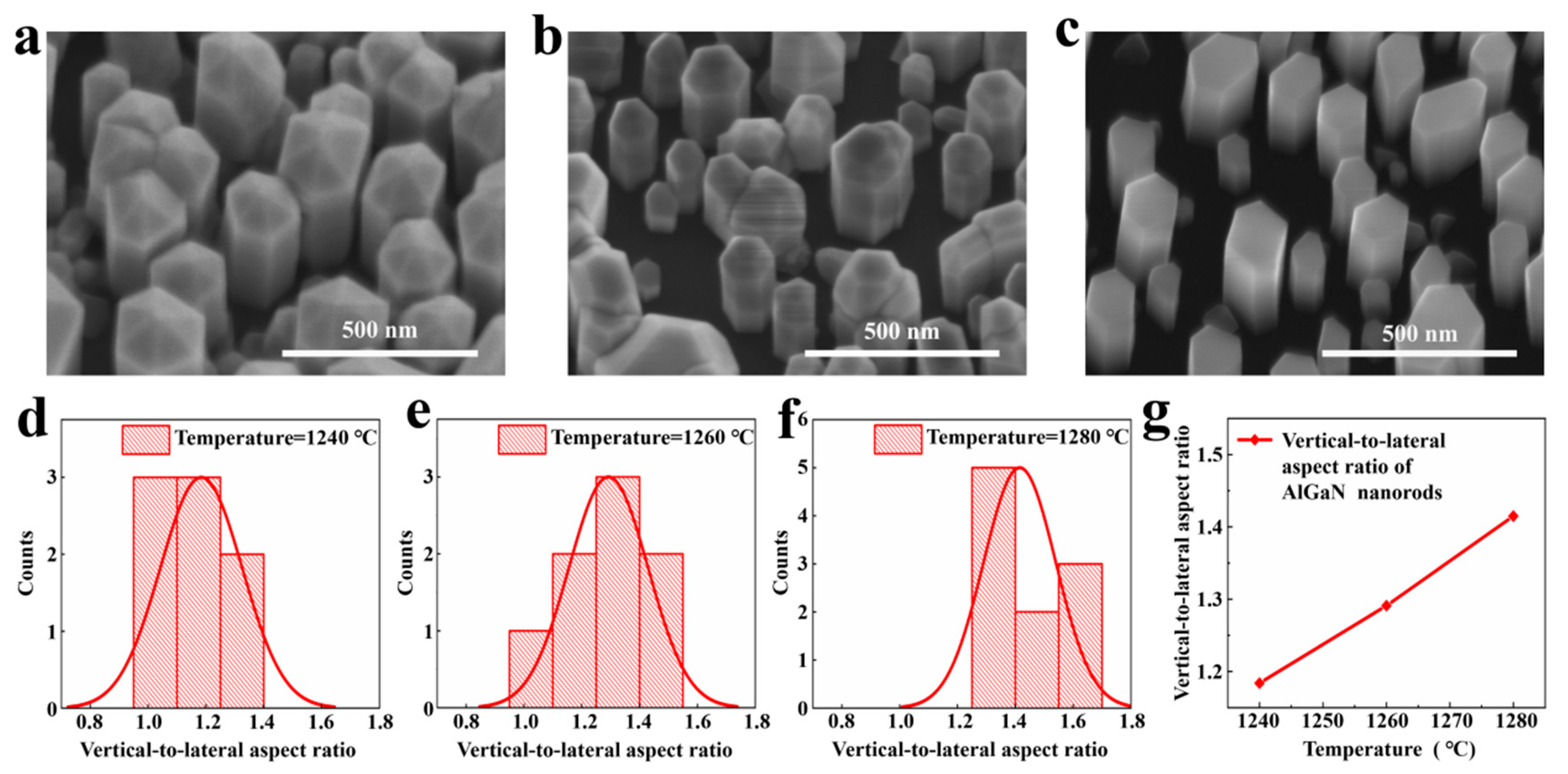
3.3. Effect of Reaction Temperature on AlGaN Nanorods

In the experiment sets A and B, it had been shown that rod-shaped AlGaN nanorods with a high aspect ratio could be obtained at low reactor pressure and low NH3 flow rate. To further gain insight into the influence of the reaction temperature on the formation of AlGaN nanorods, we designed experiment C, in which the reaction temperatures varied as 1240, 1260, and 1280 °C, and the reactor pressure and NH3 flow rate were invariably maintained at 60 Torr and 90 sccm, respectively.
When the growth temperature was 1240 °C, the AlGaN nanorods with semi-polar surfaces were observed, as illustrated in Figure 4a. According to previous reports, the as-grown face planes with the slowest growth rate determined the final morphology of the crystal [29]. Thereby, these vertically aligned AlGaN nanorods implied that the growth rate of {1–101} planes was slower than that of the c-plane. Upon increasing the reaction temperature to 1260 °C, the morphology features of the pyramidal-shaped AlGaN nanorods tip were replaced by the frustum of hexagonal pyramid structures, as shown in Figure 4b. This could be ascribed to the growth rate of the {1–101} planes improving with the increase of temperature. Afterward, the temperature was further increased to 1280 °C (Figure 4c), and the top of the AlGaN nanorods became flat, indicating that the growth rate of the c-plane exceeded that on the {1–101} plane. This might be ascribed to the fact that higher temperatures favored atoms on the semi-polar plane to gain enough energy to overcome the potential barrier and consequently accelerated the growth rate [23].
From the histogram relevant to the AlGaN nanorods buffer layer shown in Figure 4d–f, it clearly revealed that the vertical-to-lateral aspect ratio could be improved under higher reaction temperature. Furthermore, as shown in Figure 4g, the aspect ratio was proportional to the temperature.
Due to the pyramid, nanorods will maintain their shape and penetrate upward, leading to an unsmooth surface of GaN film, and the rod-like nanorods are beneficial for forming a flat and smooth surface finally. So, it is important to grow a rod-like nanorods buffer layer through adjusting the growth parameters. According to the optimized growth parameters, the condition of pressure, NH3 flow rate, and reactor temperature were set at 60 Torr, 90 sccm, and 1280 °C, respectively, to obtain good nanorods morphology for further coalescence into the flat film. On the other hand, by studying the growth rule of nanocrystals under different conditions, we found that the vertical-to-lateral aspect ratio of nanorods was enhanced with the decrease of pressure and NH3 flow rate as well as the increase of reactor temperature. However, the process of nanorods merging into films is essentially the transformation of material growth patterns from three-dimensional longitudinal growth to two-dimensional lateral growth. Consequently, during the coalescence layer growth process, the pressure, NH3 flow rate, and reactor temperature were changed to 120 Torr, 180 sccm, and 1240 °C respectively and lasted for 120 s to promote the lateral overgrowth to get a high-quality layer.

3.4. The Characterization of GaN Films

Cross-sectional TEM was carried out to investigate a detailed epi-structure of the GaN-based LEDs grown on epitaxial AlGaN nanorods buffer layer synthesized on graphene/SiO2/Si (100) substrate. Figure 5a shows a low-magnification cross-sectional TEM image of the as-grown GaN-based LEDs structure. We could clearly identify a 300 nm SiO2 substrate, 142 nm thick AlGaN nanorods/graphene buffer layers, a 450 nm thick fully coalesced GaN epilayer, an approximately 1.2 µm thick layer of n-GaN film, a MQWs active region, and a 20 nm thick layer of p-GaN, as labeled in Figure 5a,b, which displays a zoom-in image of the AlGaN nanorods buffer layer region marked with a red rectangular box in Figure 5a. The interstitial space between the AlGaN nanorods was beneficial to release the stress originated from the SiO2/Si (100) substrate, and the growth of the GaN epilayer was accomplished by controlling nanorods coalescence. Moreover, the fully coalesced GaN epilayer was almost continuous in the top of the AlGaN nanorods. The cross-sectional high-resolution TEM (HRTEM) image (Figure 5c) taken from the interface of AlGaN/graphene/SiO2 indicated the disorder of the amorphous SiO2 substrate and well-ordered and aligned crystal lattices of the crystalline AlGaN/graphene. Figure 5d illustrates the amplified MQWs active region. The abrupt interface between the five pairs of MQWs (InxGa1−xN well and GaN barrier) could be observed. The corresponding high-resolution TEM image of the GaN films region in Figure 5e presents a well-aligned crystal lattice array. Meanwhile, the lattice spacing between the adjacent planes was 0.52 nm, corresponding to the standard crystal plane spacing of GaN (0001) planes [13]. As shown in Figure 5f, the selected area electron diffraction (SAED) pattern from the GaN films shows a single diffraction pattern of the (0001) c-axis-oriented hexagonal wurtzite structure.
Figure 6a shows the smooth and flat surface, and the virtually defect-free areas of the fully coalesced GaN epilayer. Meanwhile, the SEM inset of the sample cross-section also shows that the nanorods buffer layer is clearly visible. The gaps between nanorods can help release the stress of the subsequent GaN layer. Figure 6b presents the X-ray diffraction (XRD) spectra from the as-grown GaN coalescence layer on AlGaN nanorods/graphene. It was worthy to note that the characteristic peaks were observed at approximately 34° and 72°, which was consistent with the (0002) and (0004) orientations of hexagonal wurtzite GaN, respectively. Moreover, the ω-scan rocking curves for the (002) plane illustrated in Figure 6c shows the full-width at half-maximum (FWHM) of the GaN epilayer with an AlGaN nanorods buffer layer that is estimated to be 1.74°, and the estimated density of the screw dislocations was 7.89 × 1010 cm−2.
We also investigated the stress properties of a fully coalesced GaN epilayer by Raman spectroscopy. Figure 6d shows four distinct peaks in the range between 450 and 800 cm−1. Specifically, the typical Raman modes of the GaN layer, A1 (TO), E1 (TO), and E2 (high) phonon modes were detected at 531, 557, and 566 cm−1, respectively, implying that the fully coalesced GaN epilayer was wurtzite crystal structure [30]. Furthermore, the E2 (high) phonon modes at 566 cm−1, which indicated the GaN epilayer grown on AlGaN nanorods, had slight tensile stress. The TO phonon mode at 554 or 555 cm−1 was not found in Figure 6d, indicating that there was no presence of zinc blende (cubic) GaN structure [31]. The resulting room-temperature photoluminescence (PL) exhibited intense emission at 475 nm without yellow luminescence, indicating that the as-grown LED had preferable luminescence property and low defects density. Additionally, the I-V curve of the GaN-based LEDs (Figure 6f) shows a rectifying behavior with a turn-on voltage of 5.7 V, and the inset of Figure 6f shows the optical emission from the GaN-based device with the injection current of 50 mA. The blue emitting from the LEDs device can be observed clearly. Taken together, the results as mentioned above demonstrated that good optical quality GaN-based LEDs could be grown by inserting monolayer graphene and a high-quality AlGaN nanorods buffer layer.

4. Conclusions

In summary, the growth kinetic of nitride nanorods grown on amorphous SiO2 substrate was studied to realize a continuous and flat film. We found that the morphology and vertical-to-lateral aspect ratio of nanorods could be controlled by adjusting the growth parameters via inserting the AlGaN nanorods and graphene buffer layers. In virtue of such a growth kinetic, we successfully realized continuous and flat GaN films on amorphous SiO2 substrate. The XRD, Raman, and TEM demonstrated the hexagonal wurtzite structure and aligned c-axis orientation of the GaN films. Finally, MQWs were fabricated on SiO2/Si (100) substrate and strong PL opticals, and the I-V curve shows a turn-on voltage of 5.7 V. This study provides an effective method to grow GaN-based LEDs on the amorphous substrate by integrating graphene along with the AlGaN nanorods as buffer layers, which is beneficial for the application of large-area GaN-based optoelectronic device fabrication. Meanwhile, this work also provides the possibility of integrating GaN-based optoelectronic devices with Si (100) CMOS electronics in the future.

Author Contributions

Conceptualization, W.S. and F.R.; methodology, W.S., and Y.W.; validation, W.S., F.R., and Y.Y.; formal analysis, W.S., Y.W. and B.S.; investigation, W.S. and F.R.; resources, Y.Y., S.Z. and M.L.; data curation, W.S. and T.F.; writing—original draft preparation, W.S.; writing—review and editing, W.S., F.R., Z.L. and Y.Z.; visualization, W.S., T.W., and J.W. (Jianwei Wang); supervision, J.Y., J.L. and J.W. (Junxi Wang); project administration, W.S.; funding acquisition, X.Y. and Z.L. All authors have read and agreed to the published version of the manuscript.

Funding

This research was funded by National Key R&D Program of China, grant number 2017YFB0403300, 2017YFB0403302; National Natural Science Foundation of China (61974140), (61604140).

Conflicts of Interest

The authors declare no conflict of interest.

References

  1. Akasaki, I.; Amano, H. Crystal Growth and Conductivity Control of Group III Nitride Semiconductors and Their Application to Short Wavelength Light Emitters. Jpn. J. Appl. Phys. 1997, 36, 5393–5408. [Google Scholar] [CrossRef]
  2. Chung, K.; Lee, C.-H.; Yi, G.-C. Transferable GaN Layers Grown on ZnO-Coated Graphene Layers for Optoelectronic Devices. Science 2010, 330, 655–657. [Google Scholar] [CrossRef] [PubMed]
  3. Giannazzo, F.; Fisichella, G.; Greco, G.; La Magna, A.; Roccaforte, F.; Pécz, B.; Yakimova, R.; Dagher, R.; Michon, A.; Cordier, Y. Graphene integration with nitride semiconductors for high power and high frequency electronics. Phys. Status Solidi 2016, 214, 1600460. [Google Scholar] [CrossRef]
  4. Schlotter, P.; Schmidt, R.; Schneider, J. Luminescence conversion of blue light emitting diodes. Appl. Phys. A 1997, 64, 417–418. [Google Scholar] [CrossRef]
  5. Hahn, B.; Lugauer, H.-J.; Bader, S.; Baur, J.; Eisert, D.; Strauss, U.; Zehnder, U.; Lell, A.; Hiller, N. GaN-Based LEDs and Lasers on SiC. Phys. Status Solidi 2000, 180, 5–13. [Google Scholar] [CrossRef]
  6. Mo, C.; Fang, W.; Pu, Y.; Liu, H.; Jiang, F. Growth and characterization of InGaN blue LED structure on Si(111) by MOCVD. J. Cryst. Growth 2005, 285, 312–317. [Google Scholar] [CrossRef]
  7. Wang, L.; Wang, J.; Li, H.; Xi, G.; Jiang, Y.; Zhao, W.; Han, Y.; Luo, Y. Study on Injection Efficiency in InGaN/GaN Multiple Quantum Wells Blue Light Emitting Diodes. Appl. Phys. Express 2008, 1, 21101. [Google Scholar] [CrossRef]
  8. Choi, J.H.; Zoulkarneev, A.; Kim, S.I.; Baik, C.W.; Yang, M.H.; Park, S.S.; Suh, H.; Kim, U.J.; Bin Son, H.; Lee, J.S.; et al. Nearly single-crystalline GaN light-emitting diodes on amorphous glass substrates. Nat. Photonics 2011, 5, 763–769. [Google Scholar] [CrossRef]
  9. Yu, J.; Hao, Z.-B.; Wang, J.; Deng, J.; Yu, W.; Wang, L.; Luo, Y.; Han, Y.; Sun, C.; Xiong, B.; et al. Study on AlN buffer layer for GaN on graphene/copper sheet grown by MBE at low growth temperature. J. Alloy. Compd. 2019, 783, 633–642. [Google Scholar] [CrossRef]
  10. Hayashi, H.; Konno, Y.; Kishino, K. Self-organization of dislocation-free, high-density, vertically aligned GaN nanocolumns involving InGaN quantum wells on graphene/SiO2covered with a thin AlN buffer layer. Nanotechnology 2015, 27, 55302. [Google Scholar] [CrossRef]
  11. Littlejohn, A.J.; Xiang, Y.; Rauch, E.; Lu, T.-M.; Wang, G.-C. van der Waals epitaxy of Ge films on mica. J. Appl. Phys. 2017, 122, 185305. [Google Scholar] [CrossRef]
  12. Chen, Z.; Chang, H.; Cheng, T.; Wei, T.; Wang, R.; Yang, S.; Dou, Z.; Liu, B.; Zhang, S.; Xie, Y.; et al. Direct Growth of Nanopatterned Graphene on Sapphire and Its Application in Light Emitting Diodes. Adv. Funct. Mater. 2020, 30, 2001483. [Google Scholar] [CrossRef]
  13. Chen, Z.; Zhang, X.; Dou, Z.; Wei, T.; Liu, Z.; Qi, Y.; Ci, H.; Wang, Y.; Li, Y.; Chang, H.; et al. High-Brightness Blue Light-Emitting Diodes Enabled by a Directly Grown Graphene Buffer Layer. Adv. Mater. 2018, 30, 1801608. [Google Scholar] [CrossRef] [PubMed]
  14. Li, Y.; Zhao, Y.; Wei, T.; Liu, Z.; Duan, R.; Wang, Y.; Zhang, X.; Wu, Q.; Yan, J.; Yi, X.; et al. Van der Waals epitaxy of GaN-based light-emitting diodes on wet-transferred multilayer graphene film. Jpn. J. Appl. Phys. 2017, 56, 85506. [Google Scholar] [CrossRef]
  15. Ren, F.; Yin, Y.; Wang, Y.; Liu, Z.; Liang, M.; Ou, H.; Ao, J.; Wei, T.; Yan, J.; Yuan, G.; et al. Direct Growth of AlGaN Nanorod LEDs on Graphene-Covered Si. Materials 2018, 11, 2372. [Google Scholar] [CrossRef] [Green Version]
  16. Zhao, S.; Lu, J.; Hai, X.; Yin, X. AlGaN Nanowires for Ultraviolet Light-Emitting: Recent Progress, Challenges, and Prospects. Micromachines 2020, 11, 125. [Google Scholar] [CrossRef] [Green Version]
  17. Min, J.-W.; Priante, D.; Tangi, M.; Liu, G.; Kang, C.H.; Prabaswara, A.; Zhao, C.; Al-Maghrabi, L.; Alaskar, Y.; Albadri, A.; et al. Unleashing the potential of molecular beam epitaxy grown AlGaN-based ultraviolet-spectrum nanowires devices. J. Nanophotonics 2018, 12, 43511. [Google Scholar] [CrossRef] [Green Version]
  18. Kim, J.; Bayram, C.; Park, H.; Cheng, C.-W.; Dimitrakopoulos, C.; Ott, J.A.; Reuter, K.B.; Bedell, S.W.; Sadana, D.K. Principle of direct van der Waals epitaxy of single-crystalline films on epitaxial graphene. Nat. Commun. 2014, 5, 4836. [Google Scholar] [CrossRef] [Green Version]
  19. Kovács, A.; Duchamp, M.; Dunin-Borkowski, R.E.; Yakimova, R.; Neumann, P.L.; Behmenburg, H.; Foltynski, B.; Giesen, C.; Heuken, M.; Pécz, B. Graphoepitaxy of High-Quality GaN Layers on Graphene/6H-SiC. Adv. Mater. Interfaces 2014, 2, 1400230. [Google Scholar] [CrossRef]
  20. Liu, Y.; Xu, Y.; Cao, B.; Li, Z.; Zhao, E.; Yang, S.; Wang, C.; Wang, J.; Xu, K. Transferable GaN Films on Graphene/SiC by van der Waals Epitaxy for Flexible Devices. Phys. Status Solidi 2019, 216, 1801027. [Google Scholar] [CrossRef]
  21. Mulyo, A.L.; Rajpalke, M.K.; Kuroe, H.; Vullum, P.-E.; Weman, H.; Fimland, B.-O.; Kishino, K. Vertical GaN nanocolumns grown on graphene intermediated with a thin AlN buffer layer. Nanotechnology 2018, 30, 15604. [Google Scholar] [CrossRef] [PubMed]
  22. Munshi, A.M.; Dheeraj, D.L.; Fauske, V.T.; Kim, D.-C.; Van Helvoort, A.T.J.; Fimland, B.-O.; Weman, H. Vertically Aligned GaAs Nanowires on Graphite and Few-Layer Graphene: Generic Model and Epitaxial Growth. Nano Lett. 2012, 12, 4570–4576. [Google Scholar] [CrossRef] [PubMed]
  23. Wang, Y.; Dheeraj, D.; Liu, Z.; Liang, M.; Li, Y.; Yi, X.; Wang, J.; Li, J.; Weman, H.J. AlGaN nanowires grown on SiO2/Si (100) using graphene as a buffer layer. Cryst. Growth Des. 2019, 19, 5516–5522. [Google Scholar] [CrossRef]
  24. Chae, S.J.; Seo, T.H.; Bae, J.J.; Suh, E.-K.; Yang, C.-W.; Duong, D.L.; Kim, Y.H.; Lee, S.M.; Park, M.H.; Jeong, M.S. Direct growth of etch pit-free GaN crystals on few-layer graphene. RSC Adv. 2015, 5, 1343–1349. [Google Scholar] [CrossRef]
  25. Araki, T.; Uchimura, S.; Sakaguchi, J.; Nanishi, Y.; Fujishima, T.; Hsu, A.; Kim, K.K.; Palacios, T.; Pesquera, A.; Centeno, A.; et al. Radio-frequency plasma-excited molecular beam epitaxy growth of GaN on graphene/Si(100) substrates. Appl. Phys. Express 2014, 7, 71001. [Google Scholar] [CrossRef]
  26. Lin, Y.-T.; Yeh, T.-W.; Nakajima, Y.; Dapkus, P.D. Catalyst-Free GaN Nanorods Synthesized by Selective Area Growth. Adv. Funct. Mater. 2014, 24, 3162–3171. [Google Scholar] [CrossRef]
  27. Lin, Y.-T.; Yeh, T.-W.; Dapkus, P.D. Mechanism of selective area growth of GaN nanorods by pulsed mode metalorganic chemical vapor deposition. Nanotechnology 2012, 23, 465601. [Google Scholar] [CrossRef]
  28. Willardson, R.K.; Weber, E.R.; Moustakas, T.D.; Pankove, J.I. Gallium-Nitride (GaN) II; Academic Press, 1998; Available online: https://www.elsevier.com/books/gallium-nitride-gan-ii/willardson/978-0-12-752166-4 (accessed on 5 September 2020).
  29. Song, K.M.; Kim, D.-H.; Kim, J.-M.; Cho, C.-Y.; Choi, J.; Kim, K.; Park, J.; Kim, H. White light emission of monolithic InGaN/GaN grown on morphology-controlled, nanostructured GaN templates. Nanotechnology 2017, 28, 225703. [Google Scholar] [CrossRef]
  30. Tabata, A.; Enderlein, R.; Leite, J.; Silva, A.S.; Galzerani, J.C.; Schikora, D.; Kloidt, M.; Lischka, K. Comparative Raman studies of cubic and hexagonal GaN epitaxial layers. J. Appl. Phys. 1996, 79, 4137. [Google Scholar] [CrossRef]
  31. Bülbül, M.; Smith, S.; Obradovic, B.; Cheng, T.; Foxon, C. Raman spectroscopy of optical phonons as a probe of GaN epitaxial layer structural quality. Eur. Phys. J. B 2000, 14, 423–429. [Google Scholar] [CrossRef]
Figure 1. Schematic diagram depicting the graphene transfer procedure and GaN-based light-emitting diode (LED) structure by coalescence of nanorods: (I) spin-coated poly(methyl methacrylate) (PMMA) onto the graphene membrane; (II) transfer of the PMMA/graphene membrane onto the SiO2 (300 nm)/Si wafer; (III) dissolving PMMA; (IV) growth of AlGaN nanorods by metal organic chemical vapor deposition (MOCVD); (V) coalescence of nanorods; and (VI) growth of GaN-based LED structures.
Crystals 10 00787 g001
Figure 2. Effect of reactor pressure on AlGaN nanorods: The 25° tilted-view SEM images and corresponding histogram of AlGaN nanorods profile distribution acquired with the pressure of: (a,d) 120 Torr, (b,e) 90 Torr, and (c,f) 60 Torr; (g) The vertical-to-lateral aspect ratio as a function of pressures.
Crystals 10 00787 g002
Figure 3. Effect of NH3 flow rate on AlGaN nanorods: The 25° tilted-view SEM images and corresponding histogram of AlGaN nanorods profile distribution acquired with an NH3 flow rate of (a,d) 180 sccm, (b,e) 135 sccm, and (c,f) 90 sccm; (g) the vertical-to-lateral aspect ratio as a function of NH3 flow rate.
Crystals 10 00787 g003
Figure 4. Effect of temperature on AlGaN nanorods: The 25° tilted-view SEM images and corresponding histogram of AlGaN nanorods profile distribution acquired with the temperature of: (a,d) 1240 °C, (b,e) 1260 °C, and (c,f) 1280 °C; (g) The vertical-to-lateral aspect ratio as a function of temperature.
Crystals 10 00787 g004
Figure 5. The structure of consecutive GaN-based LEDs grown on graphene/SiO2/Si (100) substrate: (a) Low-magnification cross-sectional TEM image of GaN-based LEDs growth structure; (b) The magnified view of the red box area corresponding to the AlGaN nanorods layer; (c) HRTEM taken at the interface of AlGaN/graphene/SiO2; (d) The amplified InxGa1−xN/GaN multi-quantum-wells (MQWs) structure; (e) The corresponding HRTEM image of the GaN epitaxial layer region; (f) selected area electron diffraction (SAED) pattern from the overgrown GaN layer, showing the planes of a single-crystalline wurtzite structure.
Crystals 10 00787 g005
Figure 6. The quality and optical properties of GaN films with LED structure: (a) the SEM of GaN coalescence layer grown on AlGaN nanorods/graphene; the inset shows the SEM of the sample cross-section. (b) XRD spectra of GaN coalescence layer grown on AlGaN nanorods/graphene. (c) X-ray rocking curves of (0002) GaN films grown on graphene/SiO2/Si (100) substrate with AlGaN nanorods interlayers; (d) Raman spectrum of coalesced GaN epitaxial layer. (e) Room-temperature photoluminescence (PL) spectra of GaN-based LEDs grown on graphene/SiO2/Si (100) substrate with AlGaN nanorods interlayers. (f) The current–voltage (I-V) curves of LED device; the inset shows the optical images of light emission from the LED.
Crystals 10 00787 g006
Table 1. The condition parameters for growing AlGaN nanorods of experimental sets A, B, and C.
Experimental
Set
Temperature
[℃]
NH3 Flow Rate
[sccm]
Reactor Pressure
[Torr]
A12809060–120
B128090–18060
C1240–12809060

