Article

X-ray Spectrum Reconstruction by Diamond Detectors with Linear Response to Dose Rate

by
Daniele Maria Trucchi
* and
Paolo Ascarelli
DiaTHEMA Lab, Montelibretti Unit, Istituto di Struttura della Materia ISM-CNR, Via Salaria km 29.3, 00015 Monterotondo Scalo, RM, Italy
*
Author to whom correspondence should be addressed.
Crystals 2021, 11(10), 1258; https://doi.org/10.3390/cryst11101258
Submission received: 1 September 2021 / Revised: 8 October 2021 / Accepted: 13 October 2021 / Published: 18 October 2021

Abstract

:
The absorbers method is here applied by interposing filters of variable thickness between the X-ray source and a detector so to attenuate the radiation intensity by using the attenuation coefficient as a selective photon energy operator. The analysis of the signal provided by a polycrystalline diamond thin film detector exposed to the energy-selectively-attenuated X-ray beam was used for the reconstruction of the radiation spectrum. The 50 μm thick diamond detector achieves conditions of linear response to the dose rate of the incident radiation (linearity coefficient of 0.997 ± 0.003) for a bias voltage ≥90 V, corresponding to an electric field ≥1.8 × 10⁴ V/cm. Once the absorbers method is applied, only the detector signal linearity to dose rate allows reconstructing the source X-ray bremsstrahlung spectrum with sufficiently high accuracy.

Graphical Abstract

1. Introduction

The superior diamond resistance to ionizing radiation associated with its unique electronic properties like the mobility of charge carriers, the wide bandgap energy (5.47 eV) [1] and the consequent low leakage current makes it an appealing material for the detection of photons from UV [2,3,4] to X-rays [5,6,7], charged particles [8,9,10], thermal [11] and fast neutrons [12,13,14,15]. Detectors based on diamond demonstrated a fast response [6,16] and high sensitivity [17] to X-ray beams, providing high applied electric fields with low bias voltage [18] as well as photovoltaic-mode operations [19,20], which enabled the successful application to the medical sector for the monitoring of radiation beams utilized in radiation therapy [21,22,23] and mammography [24]. Diamond films can be even utilized as suitable active material in electrochemical devices [25], radiovoltaic batteries [26,27,28,29], and concentrated solar converters [30] as well as it is an efficient electron emitter [31,32,33].
Although physical properties such as tissue equivalency and damage resistance are common to all diamond films, the electronic properties differ significantly as a function of the different film microstructures. Specifically, single-crystal films produced by chemical vapor deposition (CVD) homoepitaxy are preferred to polycrystalline films where sensitivity and fast response are required, especially for the high mobility and saturation velocity of both charge carriers connected to charge collection efficiency approaching 100% and toleration to high electric fields. However, homoepitaxial single-crystal films have a reduced size far lower than 1 cm2, limited by the diamond plate (usually a cheap high-pressure high-temperature—HPHT crystal) acting as a growth seed [34]. Another strategy has been the development of photodiodes consisting of thin p-type/intrinsic layers grown on HPHT substrates, that were successfully integrated within commercial dosimeters [35,36]. On the other hand, the promising diamond-on-iridium technology demonstrated to produce single-crystal diamond films up to almost 4 inches [37], even though the resulting film electronic properties are comparable to homoepitaxial diamond on restricted areas up to 1 cm2 [38]. As a matter of fact, today the application of single-crystal diamond is limited to the monitoring of small radiation fields as well as the relatively high cost of single-crystal diamond films hampers the practical application of more pixels in mosaic detectors. Conversely, polycrystalline diamond films can be produced by CVD heteroepitaxy, usually on crystalline silicon wafers. The mobility and collection efficiency of charge carriers is lower than single-crystal films, thus hampering the use of polycrystalline diamond detectors in pulsed mode. However, the deposition capability of polycrystalline diamond on large areas allows the fabrication of cheap detectors with a spatial resolution for large radiation fields. Another advantage of polycrystalline films is the easy separation from the growth substrate with chemical etching, which favors the development of thin films with respect to the technologically demanding cut of homoepitaxially-grown single-crystal plates, characterized by a low yield and waste of material. Moreover, the low leakage current of diamond films avoids the fabrication of complicated semiconductor architectures in favor of simple metal–diamond–metal structures, usually arranged according to a sandwich configuration with the aim to exploit all the film’s active volume. Schottky diodes or photoconductors can be fabricated as a function of the selection of the specific electrode material with respect to the specific diamond film microstructure.
The experiment here described aims at demonstrating that a polycrystalline diamond detector can be used for reconstructing the spectrum of an X-ray beam impinging on it with the use of the absorbers method. A necessary condition is that the detector should have a linear response to the energy deposited by the radiation per unit time or, equivalently, to the radiation dose rate. The idea of realizing such a spectrometry system is revisited from the experience of the crystallographers in the early twentieth century, interested in the determination of the energy spectrum distribution emitted by their X-ray sources. Indeed, differently from other methods based on the analysis of the Poisson noise of the detector signal [39] or on the stripping method [40] applied to photon-counting detectors [41] and similarly to what performed in [42] by applying the least square method, the absorbers method consists in applying an energy selective attenuation to a radiation beam by means of absorbers of different thickness. With a sufficient number n of detector signal values obtained by interposing a (n − 1) number of absorber thicknesses (which includes also the condition of absence of absorbers), it is possible to reconstruct the spectrum emitted by the radiation source, since the attenuation coefficient is an energy-dependent operator correlated to the photoelectric cross sections of the absorber and of the detector material. For such reason, the absorbers method is valid up to energies of about 100 keV, where the Compton effect is negligible for a large range of materials. The condition of response linearity to radiation dose rate for the diamond detector is not trivial to be obtained, since the electrodes and the detector size may significantly alter the correct response to the radiation dose rate. The electrodes’ thickness, usually made of metals, should be as low as possible not to induce undesired radiation absorption with unexpected energy dependence, whereas, in order to avoid lack of lateral electronic equilibrium, the electrodes’ size should approach the film surface area [43], as well as the detector size should be significantly smaller than the radiation field [44].
The aim of the present work is to demonstrate that the absorbers method, revisited by refining the model, is able to reconstruct accurately the X-ray spectrum of beams characterized by high photon fluxes, which do not allow a pulsed mode for detector signal formation but current mode. Therefore, a relatively cheap polycrystalline diamond detector can be effectively used if characterized by a linear signal to the radiation dose rate, that anyway represents the necessary condition to be satisfied by any generic detector for a correct application of the method.

2. Materials and Methods
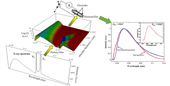
The employed X-ray beam is produced by a copper anode Philips microfocus tube, consisting of three features: the copper Kα and Kβ intensity lines (situated at the energy E = 8.05 and E = 8.90 keV, respectively) and the continuous bremsstrahlung radiation (Figure 1a). In all the experiments the copper Kβ line is almost totally suppressed by a 20 μm nickel foil, therefore the resulting radiation spectrum impinging on the diamond detector mainly consists of two contributions: the sharp copper Kα intensity line and the continuous bremsstrahlung spectrum defined for energy below the value Emax = q Vacc, where q is the elementary electron charge and Vacc the tube accelerating voltage.
The materials used as absorbers are metals of known attenuation coefficient dependence on photon energy: pure aluminum foils were used to attenuate the X-ray tube emission operating at Vacc of 30 kV, whereas pure Nichrome foils (density of 8.4 g cm−3 and nominal composition in a mass of 80% Ni – 20% Cr, data confirmed by energy-dispersive X-ray spectroscopy analysis) were used at Vacc of 40 kV. On the other hand, the cathode current was always kept at 30 mA. Considering that radiations of different energy undergo different attenuation, for an absorber of small thickness the Kα line intensity is predominant with respect to the bremsstrahlung contribution, while the opposite situation takes place at large thickness values (Figure 1b, elaborated by applying the attenuation coefficients tabulated in [45]).
The detector positioned perpendicularly to the incident radiation beam (Figure 1c) consists of a 50 μm free-standing polycrystalline diamond film with a lateral size of 8 × 8 mm2, which is far smaller than the X-ray beam diameter on the detector plane (>5 cm). The diamond film was grown by a microwave CVD system in a 0.5% methane/hydrogen concentration at 700 °C on an <100> oriented p-type silicon substrate, subsequently chemically etched in a standard HNO3:HF diluted solution in water. After the silicon etching, the diamond film was treated in a 1:1:1 HNO3:H2SO4:HClO4 solution to remove the non-diamond phases. Successively, two 200 nm thick 7 × 7 mm2 large silver contacts were thermally evaporated on the opposite sides of the film, called transversal or sandwich configuration, in order to bias the device along its bulk direction. Since the density of surface defect states of polycrystalline diamond films is able to pin the Fermi level and, in case of high defect density, to reduce the depletion region under the contacts [46], the resulting electrodes generally have a nearly ohmic behavior independently from the specific metal used. Ag was preferred to other metals for its good adhesion, stability over time, and fabrication easiness (no post-thermal annealing). The contacts’ thickness was limited to 200 nm in order not to perturb the impinging radiation spectrum. An ohmic behavior at low bias voltages <10 V and a non-linear exponential one at higher voltages were measured in the film dark current, whereas the room temperature film resistivity was measured to be >1013 Ωcm over the explored voltage range. The film was illuminated by prolonged irradiation (about 10 Gy total dose), usually called the “priming” process and aimed to saturate the deep level traps and reach the conditions of a stable response [47,48]. Under operating conditions, the detector was biased by a voltage source and the current flowing through it is measured by a picoammeter (both the functionalities were performed by a Keithley 487 instrument). The net signal produced by the device results in the subtraction of the “dark” current from the total current measured under X-ray exposure, and this operation is performed at each chosen bias voltage. The radiation dose rate was monitored by the ionization chamber Thermo Scientific (Erlangen, Germany) NE2536/3C, designed for X-ray photons and connected to the electrometer Thermo Scientific Dose Farmer mod. 2670.
For the described configuration, the radiation energy deposited per unit time in the detector depending on the absorber thickness x, f(x), can be described as:
f ( x ) 0 E max F ( E ) e α Ni ( E ) d Ni e α F ( E ) x ( 1 e α D ( E ) d ) E w   d E
where F(E) is the component of energy E of the copper emission spectrum, while the second and third terms represent the intensity transmitted by the dNi thick Nickel filter and by the absorbers, respectively, the fourth term is the fraction of intensity absorbed by the device and E/w represents the quantity of generated electron–hole pairs, being w the mean ionization energy to generate such a pair in the detector material (w = 13.1 eV in diamond [49]). αNi(E), αF(E), αD(E) are the attenuation coefficient of the Ni filter, the absorber and the diamond detector, respectively. Equation (1), performing some simple analytical steps, can be written as:
f ( x ) 0 E max F * ( E ) e α F ( E ) [ x + x 0 ]   d E ,
being F * ( E ) = F ( E ) ( 1 e α D ( E ) d ) E /   w and x 0 = d Ni α Ni ( E ) / α F ( E ) , which is a constant independent from energy since the linear attenuation coefficient dependence on photon energy of Ni and of the absorbers Nichrome and Al is proportional to the empirical kE−8/3 function (Figure 1d), where k is a constant related to the specific material. This is true until the photon absorption can be ascribed to the photoelectric effect and is generally valid up to about 100 keV also for other absorbers (e.g., Cu, Cr, Co).
As previously described, the copper emission spectrum F(E) results from the superposition of three contributions: Kα and Kβ lines, which can be mathematically modelled as delta Dirac functions δ(E) and the bremsstrahlung spectrum, that can be modelled as a continuous function of E defined for 0 ≤ EEmax and zero for E > Emax:
F ( E ) = a δ ( E E K α ) + b δ ( E E K β ) + c F bremm ( E )
being a, b, c coefficients with a constant value at each given Vacc. The introduction of the nickel filter causes the suppression of the Kβ contribution and the significant attenuation of the bremsstrahlung contribution up to 8.33 keV [45]. As a consequence, Equation (2) can be separated into two terms:
f ( x ) f K α ( x ) + f bremm ( x )
where f K α ( x ) = Φ K α F * ( E K α ) exp { α F ( E K α ) ( x + x 0 ) } is the solution of the integral for a delta Dirac function contribution, where Φ K α is a constant and f bremm ( x ) is expressed by:
f bremm ( x ) 0 E max F bremm * ( E ) e α F ( E ) [ x + x 0 ]   d E
where F bremm * ( E ) = F bremm ( E ) ( ( 1 e α D ( E ) d ) E / w ) .
It can be shown that an approximated solution of the Equation (5) is similar to that of a diffusion integral [50], with the following solution:
f bremm ( x ) = Φ bremm e α F ( E max ) ( x + x 0 ) B x + x 0
where Φbremm is a constant. This is a function of the value that αF(E) assumes at Emax, and of the B coefficient, dependent on the energy spectrum of the impinging radiation.

3. Results

Figure 2 shows the photogenerated current Iph by the detector as a function of the radiation dose rate Ď and at given bias voltage Vb, obtained by the Nichrome absorber interposition. The experimental data are fitted by Fowler’s equation Iph(Vb) ∝ ĎΔ, where Δ is the linearity coefficient that has to assume the value 1 for a detector acting as an ideal dosimeter [51]. The inset of Figure 2 shows the Δ coefficient as a function of Vb, thus highlighting that the bias voltage progressively favors the detector linearity to dose rate up to 90 V, after that the linearity remains constant since the signal practically saturates. Such behavior can be explained by considering that the collection efficiency of photogenerated charges to the electrodes increases with bias voltage, which induces a more correct signal output with respect to the energy deposited by the radiation.
Figure 3 shows plots of the device signal versus absorber thickness both for Nichrome foils (Vacc = 40 kV) and, in the inset, for aluminum ones (Vacc = 30 kV). The black thick curve represents the exact and numerically calculated solution of Equation(1), obtained by interpolating the spectrum reported in [52] for a copper target tube with a 40 kV acceleration voltage. It is again evident that at increasing voltage values the detector response tends to linearity; the experimental patterns indeed perfectly coincide with the theoretical one for a bias voltage of 90 V (1.8 × 10⁴ V/cm). For higher voltages the patterns continue to superimpose the expected linear response; this condition physically corresponds to the complete collection of all the carriers generated by the radiation. Unfortunately, owing to the lack of the tabulated copper target spectrum for an accelerating voltage of 30 kV, it is not possible to calculate the numerically exact solution of Equation (1) expected for validating the experiment with aluminum foils.
The fits shown in Figure 3 are performed by applying Equation(4), where the values of the known constants are summarized in Table 1. The fits give the values of B = 7.95 cm−1/2 and Φ/Φbremm = 1.95 × 10⁻² for Vb ≥ 90 V.
Once all the parameters have been integrated into the model and the values of B are derived from the fits, the bremsstrahlung spectrum is immediately derivable by the following expression [50]:
F bremm * ( E ) B 2 π ( α F ( E ) α F ( E max ) ) 3 / 2 e B 2 4 ( α F ( E ) α F ( E max ) ) d α F ( E ) d E
which describes the analytical function that, when integrated as in Equation (5), gives the expression f b r e m m ( x ) in Equation (6), used to fit the experimental data. Figure 4 points out the comparison between the copper bremsstrahlung spectral reconstruction and the reported spectrum in [52] as a function of radiation wavelength. We observe that the X-ray spectrum described by Equation (7) is a good approximation of the reference spectrum, showing a small underestimation for low wavelength values (high energies) mainly due to iodine contamination reported in the spectrum in literature (emission line situated at 33.17 keV) and a small overestimation for high wavelength values, which is probably due to the approximation of totally neglecting the copper Kβ intensity line in the model. However, we must recall that the absorption of the bremsstrahlung is rather small with respect to the Kα contribution (actually quantified by the f(x) tail at high x values), therefore the related error can be considered acceptable, as well as the spectral reconstruction, can be considered satisfying. The inset of Figure 4 shows the determination of the copper bremsstrahlung spectrum with Emax = 30 keV, calculated by the aluminum absorbers data.

4. Conclusions

The reported experiments highlight the importance of achieving collection efficiency able to collect all the photogenerated charges of a diamond detector by means of correct bias conditions. Different from the established literature of diamond detectors, this is demonstrated for a peculiar aim: the capability to reconstruct accurately the impinging radiation spectrum, performed by applying the revisited absorbers method and the related model, if the detector response is linear with dose rate. Under such conditions, it is possible to extract accurate spectrometry information from the detector signal. The demonstration of the method effectiveness is here limited to the reconstruction of bremsstrahlung radiation because the use of the fixed Ni filter reduced almost completely the contribution of the Cu Kβ line on the detector plane, thus hampering its reconstruction and, consequently, the comparison with the data reported in the literature. In the future, the use of variable-thickness Ni absorbers can even allow the accurate disentanglement of the Cu Kα and Kβ peaks thanks to the energy position of its absorption edge.

Author Contributions

Conceptualization, P.A.; methodology, D.M.T. and P.A.; validation, D.M.T.; formal analysis, D.M.T. and P.A.; investigation, D.M.T.; data curation, D.M.T.; writing—original draft preparation, D.M.T. and P.A.; writing—review and editing, D.M.T.; visualization, D.M.T. All authors have read and agreed to the published version of the manuscript.

Funding

This research received no external funding.

Institutional Review Board Statement

Not applicable.

Informed Consent Statement

Not applicable.

Data Availability Statement

Not applicable.

Acknowledgments

The authors thank Antonello Ranieri of IC-CNR for the highly valuable technical support.

Conflicts of Interest

The authors declare no conflict of interest.

References

  1. Sussmann, R.S. CVD Diamond for Electronic Devices and Sensors; John Wiley & Sons Ltd.: London, UK, 2009. [Google Scholar]
  2. Liu, Z.; Zhao, D.; Zhu, T.; Wang, J.; Yi, W.; Min, T.; Wang, H. Enhanced Responsivity of Diamond UV Detector Based on Regrown Lens Structure. IEEE Electron Device Lett. 2020, 41, 1829–1832. [Google Scholar] [CrossRef]
  3. Almaviva, S.; Marinelli, M.; Milani, E.; Prestopino, G.; Tucciarone, A.; Verona, C.; Verona-Rinati, G.; Angelone, M.; Pillon, M. Extreme UV single crystal diamond Schottky photodiode in planar and transverse configuration. Diam. Relat. Mater. 2010, 19, 78–82. [Google Scholar] [CrossRef]
  4. Liu, K.; Wang, W.; Dai, B.; Yang, L.; Zhao, J.; Xue, J.; Liu, B.; Lv, Z.; Bi, M.; Shu, G.; et al. Impact of UV spot position on forward and reverse photocurrent symmetry in a gold-diamond-gold detector. Appl. Phys. Lett. 2018, 113, 023501. [Google Scholar] [CrossRef]
  5. Bloomer, C.; Newton, M.E.; Rehm, G.; Salter, P.S. A single-crystal diamond X-ray pixel detector with embedded graphitic electrodes. J. Synchrotron Radiat. 2020, 27, 599–607. [Google Scholar] [CrossRef] [PubMed]
  6. Liu, L.Y.; Ouyang, X.P.; Zhang, J.F.; Jin, P.; Su, C.L. Properties comparison between nanosecond X-ray detectors of polycrystalline and single-crystal diamond. Diam. Relat. Mater. 2017, 73, 248–252. [Google Scholar] [CrossRef]
  7. Marinelli, M.; Milani, E.; Prestopino, G.; Verona, C.; Verona-Rinati, G.; Angelone, M.; Pillon, M.; Kachkanov, V.; Tartoni, N.; Benetti, M.; et al. X-ray beam monitor made by thin-film CVD single-crystal diamond. J. Synchrotron Radiat. 2012, 19, 1015–1020. [Google Scholar] [CrossRef] [Green Version]
  8. Tchouaso, M.T.; Kasiwattanawut, H.; Prelas, M.A. Energy response of diamond sensor to beta radiation. Appl. Radiat. Isot. 2018, 139, 66–69. [Google Scholar] [CrossRef]
  9. Chaudhuri, S.K.; Kleppinger, J.W.; Karadavut, O.; Mandal, K.C. Behavioral Contrast of Electron and Hole Transport in High-Resolution Diamond Detectors: A Biparametric Correlation Study. IEEE Electron Device Lett. 2021, 42, 200–203. [Google Scholar] [CrossRef]
  10. Bäni, L.; Alexopoulos, A.; Artuso, M.; Bachmair, F.; Bartosik, M.; Beck, H.; Bellini, V.; Belyaev, V.; Bentele, B.; Bes, A.; et al. A study of the radiation tolerance of poly-crystalline and single-crystalline CVD diamond to 800 MeV and 24 GeV protons. J. Phys. D Appl. Phys. 2019, 52, 465103. [Google Scholar] [CrossRef]
  11. Holmes, J.; Brown, J.; Koeck, F.A.; Johnson, H.; Benipal, M.K.; Kandlakunta, P.; Zaniewski, A.; Alarcon, R.; Cao, R.; Goodnick, S.M.; et al. Performance of 5-μm PIN diamond diodes as thermal neutron detectors. Nuclear Instrum. Methods Phys. Res. Sect. A Accel. Spectrom. Detect. Assoc. Equip. 2020, 961, 163601. [Google Scholar] [CrossRef]
  12. Muraro, A.; Giacomelli, L.; Nocente, M.; Rebai, M.; Rigamonti, D.; Belli, F.; Calvani, P.; Figueiredo, J.; Girolami, M.; Gorini, G.; et al. First neutron spectroscopy measurements with a pixelated diamond detector at JET. Rev. Sci. Instrum. 2016, 87, 11D833. [Google Scholar] [CrossRef] [Green Version]
  13. Girolami, M.; Bellucci, A.; Calvani, P.; Cazzaniga, C.; Rebai, M.; Rigamonti, D.; Tardocchi, M.; Pillon, M.; Trucchi, D.M. Mosaic diamond detectors for fast neutrons and large ionizing radiation fields. Phys. Status Solidi (A) 2015, 212, 2424–2430. [Google Scholar] [CrossRef]
  14. Angelone, M.; Pilotti, R.; Stacchi, F.; Pillon, M.; Klix, A.; Raj, P.; Loreti, S.; Pagano, G. Performance test of radiation detectors developed for ITER-TBM. Fusion Eng. Des. 2018, 136, 1386–1390. [Google Scholar] [CrossRef]
  15. Claps, G.; Murtas, F.; Foggetta, L.; Di Giulio, C.; Alozy, J.; Cavoto, G. Diamondpix: A CVD Diamond Detector With Timepix3 Chip Interface. IEEE Trans. Nuclear Sci. 2018, 65, 2743–2753. [Google Scholar] [CrossRef]
  16. Trucchi, D.M.; Allegrini, P.; Calvani, P.; Galbiati, A.; Oliver, K.; Conte, G. Very Fast and Priming-less Single-Crystal Diamond X-ray Dosimeters. IEEE Electron Device Lett. 2012, 33, 615–617. [Google Scholar] [CrossRef]
  17. Trucchi, D.M.; Allegrini, P.; Bellucci, A.; Calvani, P.; Galbiati, A.; Girolami, M. Resistant and sensitive single-crystal diamond dosimeters for ionizing radiation. Nuclear Instrum. Methods Phys. Res. Sect. A Accel. Spectrom. Detect. Assoc. Equip. 2013, 718, 373–375. [Google Scholar] [CrossRef]
  18. Pomorski, M.; Caylar, B.; Bergonzo, P. Super-thin single crystal diamond membrane radiation detectors. Appl. Phys. Lett. 2013, 103, 112106. [Google Scholar] [CrossRef] [Green Version]
  19. Bellucci, A.; Orlando, S.; Caputo, D.; Cappelli, E.; Trucchi, D.M. Dosimetric Performance of Single-Crystal Diamond X-Ray Schottky Photodiodes. IEEE Electron Device Lett. 2013, 34, 695–697. [Google Scholar] [CrossRef]
  20. Conte, G.; Spadaro, S.; Di Castro, E.; Carni, M. Zero-bias operation and beam energy dependence of diamond sensors. Key Eng. Mater. 2013, 543, 426–430. [Google Scholar] [CrossRef]
  21. Talamonti, C.; Kanxheri, K.; Pallotta, S.; Servoli, L. Diamond Detectors for Radiotherapy X-Ray Small Beam Dosimetry. Front. Phys. 2021, 9, 112. [Google Scholar] [CrossRef]
  22. Marinelli, M.; Prestopino, G.; Verona, C.; Verona-Rinati, G.; Ciocca, M.; Mirandola, A.; Mairani, A.; Raffaele, L.; Magro, G. Dosimetric characterization of a microDiamond detector in clinical scanned carbon ion beams. Med. Phys. 2015, 42, 2085. [Google Scholar] [CrossRef] [Green Version]
  23. Scaringella, M.; Zani, M.; Baldi, A.; Bucciolini, M.; Pace, E.; de Sio, A.; Talamonti, C.; Bruzzi, M. First dose-map measured with a polycrystalline diamond 2D dosimeter under an intensity modulated radiotherapy beam. Nuclear Instrum. Methods Phys. Res. Sect. A Accel. Spectrom. Detect. Assoc. Equip. 2015, 796, 89–92. [Google Scholar] [CrossRef]
  24. Ade, N. An investigation of the role of defect levels on the radiation response of synthetic diamond crystals when used as sensors for the detection of mammography X-rays. Appl. Radiat. Isot. 2017, 127, 237–244. [Google Scholar] [CrossRef] [PubMed]
  25. Sartori, A.F.; Orlando, S.; Bellucci, A.; Trucchi, D.M.; Abrahami, S.; Boehme, T.; Hantschel, T.; Vandervorst, W.; Buijnsters, J.G. Laser-Induced Periodic Surface Structures (LIPSS) on Heavily Boron-Doped Diamond for Electrode Applications. ACS Appl. Mater. Interfaces 2018, 10, 43236–43251. [Google Scholar] [CrossRef] [PubMed] [Green Version]
  26. Delfaure, C.; Pomorski, M.; de Sanoit, J.; Bergonzo, P.; Saada, S. Single crystal CVD diamond membranes for betavoltaic cells. Appl. Phys. Lett. 2016, 108, 252105. [Google Scholar] [CrossRef]
  27. Trucchi, D.M.; Cappelli, E.; Lisi, N.; Ascarelli, P. Feasibility of CVD diamond radiation energy conversion devices. Diam. Relat. Mater. 2006, 15, 1980–1985. [Google Scholar] [CrossRef]
  28. Bormashov, V.S.; Troschiev, S.Y.; Tarelkin, S.A.; Volkov, A.P.; Teteruk, D.V.; Golovanov, A.V.; Kuznetsov, M.S.; Kornilov, N.V.; Terentiev, S.A.; Blank, V.D. High power density nuclear battery prototype based on diamond Schottky diodes. Diam. Relat. Mater. 2018, 84, 41–47. [Google Scholar] [CrossRef]
  29. Mackenzie, G.R.; Kaluvan, S.; Martin, P.G.; Hutson, C.; Connolley, T.; Cattelan, M.; Dominguez-Andrade, H.; Martin, T.L.; Fox, N.A.; Scott, T.B. A diamond gammavoltaic cell utilizing surface conductivity and its response to different photon interaction mechanisms. Mater. Today Energy 2021, 21, 100688. [Google Scholar] [CrossRef]
  30. Trucchi, D.M.; Bellucci, A.; Girolami, M.; Calvani, P.; Cappelli, E.; Orlando, S.; Polini, R.; Silvestroni, L.; Sciti, D.; Kribus, A. Solar Thermionic-Thermoelectric Generator (ST2G): Concept, Materials Engineering, and Prototype Demonstration. Adv. Energy Mater. 2018, 8, 1802310. [Google Scholar] [CrossRef]
  31. Trucchi, D.M.; Scilletta, C.; Cappelli, E.; Merli, P.; Zoffoli, S.; Mattei, G.; Ascarelli, P. Optimization of the performance of CVD diamond electron multipliers. Diam. Relat. Mater. 2006, 15, 827–832. [Google Scholar] [CrossRef]
  32. Velardi, L.; Turco, V.; Monteduro, L.; Cicala, G.; Valentini, A.; Nassisi, V. Electron beams produced by innovative photocathodes based on nanodiamond layers. Phys. Rev. Accel. Beams 2019, 22, 093402. [Google Scholar] [CrossRef] [Green Version]
  33. Ukraintsev, E.; Kromka, A.; Janssen, W.; Haenen, K.; Takeuchi, D.; Bábor, P.; Rezek, B. Electron emission from H-terminated diamond enhanced by polypyrrole grafting. Carbon 2021, 176, 642–649. [Google Scholar] [CrossRef]
  34. Balmer, R.S.; Brandon, J.R.; Clewes, S.L.; Dhillon, H.K.; Dodson, J.M.; Friel, I.; Inglis, P.N.; Madgwick, T.D.; Markham, M.L.; Mollart, T.P.; et al. Chemical vapour deposition synthetic diamond: Materials, technology and applications. J. Phys. Condens. Matter Inst. Phys. J. 2009, 21, 364221. [Google Scholar] [CrossRef] [PubMed] [Green Version]
  35. Almaviva, S.; Ciancaglioni, I.; Consorti, R.; De Notaristefani, F.; Manfredotti, C.; Marinelli, M.; Milani, E.; Petrucci, A.; Prestopino, G.; Verona, C.; et al. Synthetic single crystal diamond dosimeters for Intensity Modulated Radiation Therapy applications. Nuclear Instrum. Methods Phys. Res. Sect. A Accel. Spectrom. Detect. Assoc. Equip. 2009, 608, 191–194. [Google Scholar] [CrossRef]
  36. Zani, M.; Bucciolini, M.; Casati, M.; Talamonti, C.; Marinelli, M.; Prestopino, G.; Tonnetti, A.; Verona-Rinati, G. A synthetic diamond diode in volumetric modulated arc therapy dosimetry. Med. Phys. 2013, 40, 092103. [Google Scholar] [CrossRef] [Green Version]
  37. Schreck, M. 3.11-Single Crystal Diamond Growth on Iridium. In Comprehensive Hard Materials; Sarin, V.K., Ed.; Elsevier: Oxford, UK, 2014; pp. 269–304. [Google Scholar]
  38. Berdermann, E.; Afanaciev, K.; Ciobanu, M.; Fischer, M.; Gsell, S.; Kiš, M.; Lagomarsino, S.; Lohmann, W.; Mayr, M.; Pomorski, M.; et al. Progress in detector properties of heteroepitaxial diamond grown by chemical vapor deposition on Ir/YSZ/Si(001) wafers. Diam. Relat. Mater. 2019, 97, 107420. [Google Scholar] [CrossRef]
  39. Li, R.; Li, L.; Chen, Z. Spectrum reconstruction method based on the detector response model calibrated by x-ray fluorescence. Phys. Med. Biol. 2017, 62, 1032–1045. [Google Scholar] [CrossRef]
  40. Michel, T.; Talla, P.T.; Firsching, M.; Durst, J.; Bohnel, M.; Anton, G. Reconstruction of X-ray spectra with the energy sensitive photon counting detector Medipix2. Nuclear Instrum. Methods Phys. Res. A 2009, 598, 510–514. [Google Scholar] [CrossRef]
  41. Ponchut, C. Correction of the charge sharing in photon-counting pixel detector data. Nuclear Instrum. Methods Phys. Res. Sect. A Accel. Spectrom. Detect. Assoc. Equip. 2008, 591, 311–313. [Google Scholar] [CrossRef]
  42. Cao, J.; Jiang, C.-Y.; Zhao, Y.-F.; Yang, Q.-W.; Yin, Z.-J. A novel X-ray tube spectra reconstruction method based on transmission measurements. Nuclear Sci. Tech. 2016, 27, 45. [Google Scholar] [CrossRef]
  43. Marsolat, F.; Tromson, D.; Tranchant, N.; Pomorski, M.; Bassinet, C.; Huet, C.; Derreumaux, S.; Chea, M.; Cristina, K.; Boisserie, G.; et al. Why diamond dimensions and electrode geometry are crucial for small photon beam dosimetry. J. Appl. Phys. 2015, 118, 234507. [Google Scholar] [CrossRef]
  44. Ade, N.; Nam, T.L. The influence of detector size relative to field size in small-field photon-beam dosimetry using synthetic diamond crystals as sensors. Radiat. Phys. Chem. 2015, 113, 6–13. [Google Scholar] [CrossRef]
  45. Hubbell, J.H.; Seltzer, S.M. X-Ray Mass Attenuation Coefficients. NISTIR 5632 2004. [Google Scholar] [CrossRef]
  46. Conte, G.; Rossi, M.C.; Salvatori, S.; Fabbri, F.; Loreti, S.; Ascarelli, P.; Cappelli, E.; Trucchi, D. Grain boundary transport in x-ray irradiated polycrystalline diamond. J. Appl. Phys. 2003, 93, 6078. [Google Scholar] [CrossRef]
  47. Bruzzi, M.; Menichelli, D.; Sciortino, S.; Lombardi, L. Deep levels and trapping mechanisms in chemical vapor deposited diamond. J. Appl. Phys. 2002, 91, 5765. [Google Scholar] [CrossRef] [Green Version]
  48. Behnke, T.; Oh, A.; Wagner, A.; Zeuner, W.; Bluhm, A.; Klages, C.P.; Paul, M.; Schafer, L. Development of diamond films for particle detector applications. Diam. Relat. Mater. 1998, 7, 1553–1557. [Google Scholar] [CrossRef]
  49. Shimaoka, T.; Kaneko, J.H.; Sato, Y.; Tsubota, M.; Shimmyo, H.; Chayahara, A.; Watanabe, H.; Umezawa, H.; Mokuno, Y. Fano factor evaluation of diamond detectors for alpha particles. Phys. Status Solidi (A) 2016, 213, 2629–2633. [Google Scholar] [CrossRef]
  50. Greening, J.R. The Determination of X-Ray Wavelength Distributions from Absorption Data. Proc. Phys. Soc. A 1950, 63, 1227–1234. [Google Scholar] [CrossRef]
  51. Fowler, J.F.; Attix, F.H. Solid state electrical conductivity dosimeters. In Radiation Dosimetry, 2nd ed.; Attix, F.H., Roesch, W.C., Eds.; Academic Press: New York, NY, USA, 1966. [Google Scholar]
  52. Macgillavry, C.H.; Rieck, G.D. International Tables For X-ray Crystallography; Volume 3: Physical and Chemical Tables; Kynoch Press for the International Union of Crystallography: Birmingham, UK, 1962; p. 362. [Google Scholar]
Figure 1. (a) The intensity spectrum of the X-ray beam produced by the copper anode tube supplied at Vacc (Emax = q Vacc and λmin = 1240/Emax) passes through a nickel filter in order to suppress the Kβ line (b) and then the radiation intensity is attenuated by the absorbers (Nichrome in the 3D plot) characterized by a defined thickness x. (c) Finally, the beam impinges perpendicularly on the diamond sandwich detector, biased along the bulk direction. (d) The attenuation coefficient dependences on photon energy of diamond, Ni, Al and Nichrome absorbers denote the common E−8/3 dependence up to about 100 keV, as well as the characteristic absorption edges typical of each specific material.
Crystals 11 01258 g001
Figure 2. The detector signal to dose rate dependence. The experimental points are well fitted by Fowler’s equation. Inset: the value of the Δ coefficient tends to the unity for a voltage corresponding to the signal saturation region (≥90 V), approaching the behavior of an ideal dosimeter.
Crystals 11 01258 g002
Figure 3. Plot of the detector signal versus absorber thickness as a function of the applied bias voltage. The continuous thick curve, almost superimposing the signal at Vb ≥ 90 V, represents the exact solution of Equation (1).
Crystals 11 01258 g003
Figure 4. Comparison between the reconstructed and the reported bremsstrahlung distribution as a function of radiation wavelength for X-rays produced at 40 kV by a copper-target tube (30 kV in the inset).
Crystals 11 01258 g004
Table 1. Values of known coefficients derivable from [45] for Nichrome and aluminum absorbers.
Model/Fit ParameterUnitsNichrome AbsorbersAluminum Absorbers
EmaxkeV4030
αNi(E)cm−1432.8432.8
αD(E)cm−116.116.1
αF(E)cm−1746.1135.7
αF(Emax)cm−135.83.04
x0cm2.13 × 10−35.11 × 10⁻²
Publisher’s Note: MDPI stays neutral with regard to jurisdictional claims in published maps and institutional affiliations.

