1. Introduction
Semiconductor-based transistors have been invented and first demonstrated by J. Bardeen and W.H. Brattain in 1948 [
1]. Five years later, J.N. Shive published the first Ge-based photo-transistor [
2,
3]. Many years thereafter, in 1993, M.A. Khan demonstrated the first GaN-based high electron-mobility transistor (HEMT) in enhancement mode [
4]. Thanks to the advent of the InGaN-based blue laser diode, the topic of nitride-based semiconductor alloys has again gained considerable momentum [
5,
6,
7,
8,
9]. Since semiconductor laser diodes allowed—from 1962 onward—the generation of high-frequency modulated optical signals [
10], a robust and ultra-fast phototransistor working at the optical telecommunication wavelength of 1.55 µm would constitute a major breakthrough. In this paper, we, therefore, present the design and simulation of a GaN/AlN-based, rugged and fast phototransistor with a 1.55 µm inter-subband detector acting on the transistor gate. In this type of device, the absence of a p-n-junction, hence of a space charge region, lifts one big, omnipresent problem of bipolar transistors: In terms of limiting frequency, bipolar devices always hit a ‘hard stop’ defined by their parasitic capacitance. However, inter-subband devices do not suffer from this particular limitation. Therefore, the maximal bandwidth of such a photo-transistor can be pushed to very high values.
In order to resolve the doubly unfavorable situation of having (as described in [
11]) a photo-detector with a bandwidth limited to 3 GHz and a responsivity of 10 mV/W, we propose several crucially important improvements. The first one is the use of a sufficiently small area 1.55 µm inter-subband (ISB) photo-detector. As a second important point, a more sophisticated mounting scheme must be used. It will avoid large area metal contacts as much as long wire bonds. These first two measures taken together will reduce both the parasitic capacitance and inductance values of our device; and thus, substantially increase its rollover frequency. As a third improvement, a short, but ultra-strongly coupled (
κL > 1) second-order ‘enhanced coupling strength’ (ECS) diffraction grating—allowing vertical incidence of the incoming radiation—will be fabricated on top of the elongated gate contact. In order to facilitate its fabrication, Schottky metal stripes with a period of 625 nm at 50% filling factor will be thermally evaporated. As a fourth and probably most important measure, the presented superlattice (SL) detector will become the gate region of a monolithically integrated, normally-off HFET [
12]. This strategy will boost the existing signal size to a usefully large value. In order to pave the way for a practical realization of these propositions, we present here a simple model which predicts correct device operation at modulation frequencies of up to 100 GHz.
2. Device Design and Experimental Considerations
This paragraph starts with a brief overview of both design and performance of those GaN-based ISB detectors which have been demonstrated up to now. A more comprehensive description can be found in reference [
11]. In a nutshell, the epitaxial layers are grown on top of a C-face sapphire substrate. Growth conditions are chosen to result in N-polarity for all layers. The first layer is a 4 µm thick, undoped AlN buffer which is deposited by metal-organic vapor phase epitaxy (MOVPE). On top of this buffer layer, the active device structure is grown by plasma-assisted molecular beam epitaxy (PA-MBE). It is based on 100 GaN QWs with a thickness of 1.5 nm each, a high Si-doping level of 5 × 10
19 cm
−3, and 15 nm thick undoped AlN barriers in between. In our experiments described for instance in reference [
11], this SL is covered with an undoped AlN cap layer, whose ideal thickness will here be determined experimentally. In the year 2012, it became evident that the underlying mechanism of these detectors is in fact ‘nonlinear optical rectification’; described for the first time by Emmanuel Rosencher and Philippe Bois in 1991 [
13]. One important note concerns the mode of operation of these devices. In a photo-conductive detector such as a p-n-junction under standard operating conditions, the responsivity is given in units of [
A/W]. However, the proposed inter-subband device works as a photo-voltaic detector [
14]. In this case, the voltage responsivity—defined by
is measured in units of [
V/W]. In Equation (1),
is the optical rectification voltage,
= 1.5 nm the
QW thickness,
the static dielectric constant of GaN,
the refractive index of GaN,
8.85 × 10
−12 As/Vm the vacuum permittivity,
= 370 fs the lifetime of the involved transition [
9],
= 3 Å the mean lateral electron displacement,
=
the volume carrier density,
= 3.1 Å the transition matrix element,
q = 1.602 × 10
−19 C the elementary charge,
= 1.054 × 10
−34 Js Planck’s constant,
the electrical field of the focalized illuminating radiation (
P = 10 mW on a round spot with a diameter of about 60 µm),
= 80% the diffraction efficiency of the second-order enhanced coupling strength (ECS) grating [
15], and 2
Γ = 80 meV the full width at half maximum of the involved transition.
Compared to our previous work [
11], a larger number of
QWs, thicker barrier layers, and a highly efficient ECS grating are used. These changes lead to a noticeable decrease of the parasitic capacitance, and a considerably larger detector bandwidth.
Inter-subband absorption is not only interesting from a physics point-of-view, it is also very well suited for high-frequency applications. The drawback, however, is the low signal produced. In order to increase its size, the presented detector will now become the gate region of a monolithically integrated, photo-induced HFET. This HFET will be operated in enhancement (normally-off) mode. For this purpose, the entire SL serves as a transistor channel, while a 6 nm-thick Al
0.25Ga
0.75N-based (transistor) barrier and a 25 nm-thick p-GaN cap layer (Mg: N
A = 2 × 10
19 cm
−3) are epitaxially grown on top. At zero gate voltage, the p-type cap guarantees a complete depletion of the 2-DEG. In order to couple the incoming radiation efficiently to the gate, a metallic second-order diffraction grating with a period of Λ = 0.625 µm and a metal thickness of
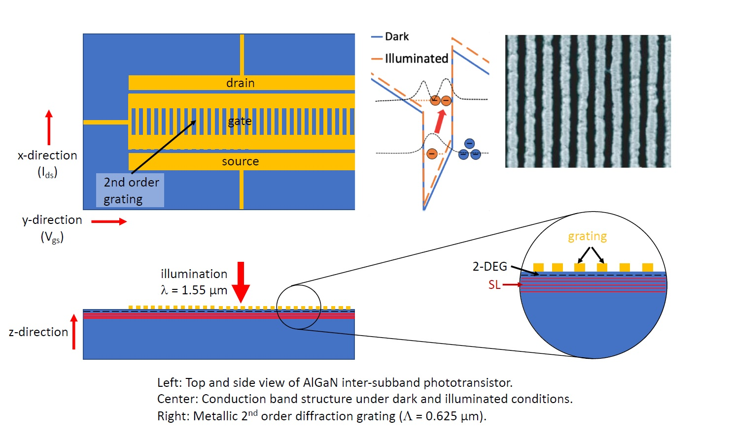
t = 0.21 µm will be defined on the gate. The general architecture of the proposed device is presented in the schematic drawing of
Figure 1.
A gate length (equivalent to the grating width) of Lgate = dgrating = 2 µm with an elongated linear grating length of dgate = Lgrating = 25 µm will be fabricated. Thanks to a so-called ‘enhanced coupling strength’ (ECS) metal grating, even such tight grating dimensions guarantee an extremely high coupling efficiency of roughly 80%, a sufficiently small device area, and thus a high operating bandwidth. On either side of the grating lines, long contiguous metal stripes will be deposited. They will be used for an additional application of a constant gate bias. The metal layers will be the same as for the Schottky metallization (Ti/Au with layer thicknesses of 10/200 nm). On top of the metal grating, a 50 nm thick low refractive index ‘liner layer’ (i.e., SiO2) followed by a 1 µm thick high index ‘cover layer’ (i.e., amorphous Si) have to be deposited to enhance the grating’s coupling strength.
The quantum efficiency of the photo-transistor is related to the diffraction efficiency of the ECS grating on the gate region, for which we estimated η = 80%. The transistor’s overall quantum efficiency at 150 K is therefore 4 mV/W. At 300 K, the corresponding value drops to 0.25 mV/W. The 3 dB-frequency of this device is—as mentioned above—in the range of f3dB = 100 GHz. This is equivalent to rise- and fall-times of 3.5 ps.
3. Simulation
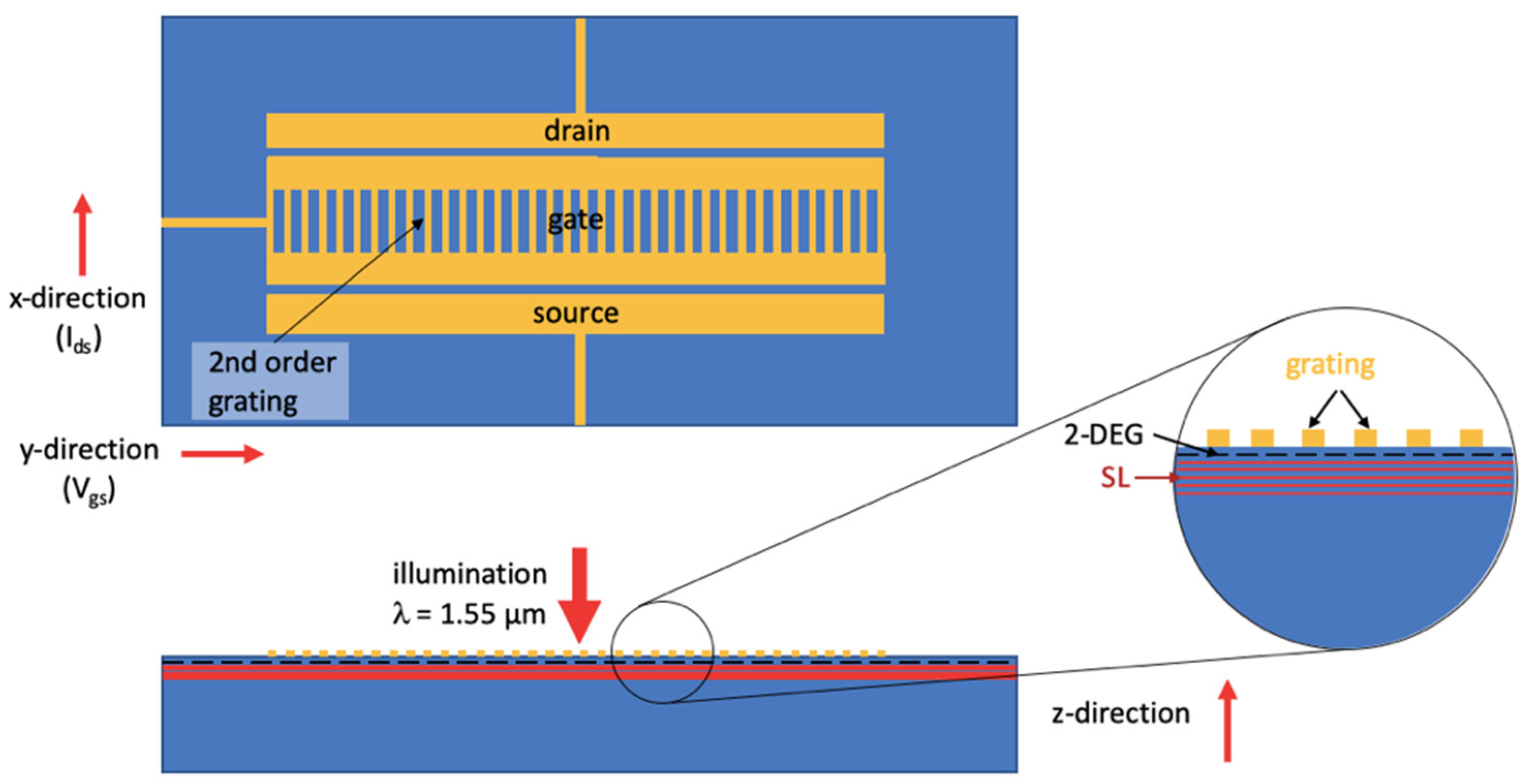
The working principle of this optically induced HFET is schematically shown by its conduction band structure in
Figure 2.
The solid line in blue color illustrates the situation without illumination, whereas the dashed orange line corresponds to the structure under illumination. The moduli squared of the relevant bound state wavefunctions are shown as well. Red arrows illustrate the slightly diagonal electronic transition under optical excitation. For a better visualization, the optical rectification voltage has been exaggerated by a factor of 1000. Evidently, the excitation of electrons induces a change of both the electron concentration of the 2-DEG layer and thus the channel transconductance. By applying a constant bias voltage of either +0.0 V, +0.5 V, +1.0 V, +1.5 V, or +2.0 V on the gate, an experimental determination of the working point of this enhancement-mode HFET will be done. Typical values of the transconductance and the expected source-drain current changes, both normalized to the gate length, are presented in
Table 1. The cited numbers were taken from a paper by Palacios et al. about an enhancement-mode HFET having a p-GaN gate [
16] and using V
ds = 5 V.
Expressed in other words, the ideal condition will be the electrical gate bias V
gs,el, at which the transconductance—defined by g
m = I
ds,el/V
gs,el—reaches its maximal value of g
m = 420 mS/mm. For the enhancement-mode HFET cited above in reference [
16], this is the case for an electrical gate bias of V
gs,el = +1.0 V. At this gate voltage and a drain voltage of V
ds = +5.0 V, the differential source-drain current can then be calculated according to the formulae shown as shown below:
Here, ηgs,or = 3.25 mV/W (0.25 mV/W) is the initial detector responsibility at 150 K (300 K)—serving as transistor gate voltage. Compared to our article from 2009, these values are considerably larger. This is due to a factor of 2.5 in the number of active region periods and a factor of 8 in the diffraction efficiency, whose elevated value is—in the present work—provided by an ECS grating. Vgs,el = +1.0 V is the dc bias on the electrical gate voltage necessary to achieve maximal transconductance, Ids,el is the illumination-independent drain-source current due to the electrical gate voltage, gm = 420 mS/mm (gm = 100 mS/mm) the maximally possible transconductance at 150 K (300 K), dgrating = Lgate = 2 µm the gate length, Lgrating = dgate = 25 µm the gate width, Popt = 10 mW the optical input power, and ηcoupler = 80% the diffraction efficiency of the second-order ECS grating. Finally, ∆Ids,or is the drain current due to optical rectification alone. In Equations (2)–(4), it is important to subtract the drain-source current due to the constant electrical gate voltage (Ids,el). For Vgs,el = +1.0 V (0.0 V), this results in a normalized net source-drain current change of ∆Ids,or = 10.92 µA/mm (0.84 µA/mm). For a typical gate length of 2 µm, we therefore calculate at 1.0 V (0.0 V) gate voltage a source-drain current of 21.84 nA (1.68 nA). Current values of that order of magnitude can be measured with a high-quality current amplifier—for instance with a ‘Stanford Research Systems’ (model SR570)—which allows setting a much more sensitive current gain level of 1 pA/V. At zero electrical gate voltage (Vgs,el = +0.0 V), a factor of 17 smaller source-drain currents of ∆Ids,or = 1.3 nA (0.1 nA) would occur.
A crucial issue will be the efficient rejection of visible and UV wavelengths. This is especially important because of the high bandgap of GaN and AlGaN. For this purpose, three different mechanisms will be exploited—taking advantage of direction, energy, and polarization.
First, a directional discrimination is achieved using a second-order diffraction grating for 1.55 µm (or 800 meV). Incoming light at angles different from perpendicular to the surface will after diffraction not end up propagating horizontally—and will, therefore, not be absorbed.
Second, energy discrimination is obtained via inter-subband absorption in appropriately designed GaN QWs. Based on our earlier experimental results, a GaN-based QW with a thickness of 1.5 nm (along with 15 nm thick AlN barriers) leads to absorption at the optical telecommunication wavelength of 1.55 µm or 800 meV. In addition, the narrow stopband of the diffraction grating provides an additional, precise energy selection (typically Δλ/λ < 1 × 10⁻²).
Third, polarization discrimination is provided by the use of QW-based inter-subband absorption. Owing to the quantum-mechanical polarization selection rule, only TM polarized radiation can strongly interact with the QWs.
Below the GaN bandgap (hν < 3.4 eV), all wavelengths will pass the QW region without any interaction. The only exception from this rule is a relatively narrow wavelength range corresponding to the QW inter-subband transition energy. There, strong absorption will occur.
Above the GaN bandgap (hν > 3.4 eV), all wavelengths will be strongly absorbed by the QWs. In order to prevent any unwanted absorption of interband radiation at these visible and UV wavelengths, it is necessary to insert a long-pass filter into the optical path. Alternatively, this filter can be evaporated directly on top of the grating.
4. Results
By conservatively assuming that the practical lower measurement limit of the source-drain current is a factor of 220 smaller than the 22 nA cited above—thus 100 pA—then this latter value is still 100 times as large as the specified lower current limit (1 pA) producing 1 V of output signal. In addition, the ‘Stanford model SR570’ current amplifier allows a constant offset of the illumination independent part of the source-drain current while the illumination-dependent current alone is amplified. Based on this reasoning (and at a temperature of 150 K), optical intensities as small as 10 µW can be measured safely. At 300 K, where the optical rectification signal will be roughly a factor of 10 smaller than at 150 K, the detection limit will—in an inversely proportional dependence—increase to roughly 100 µW.
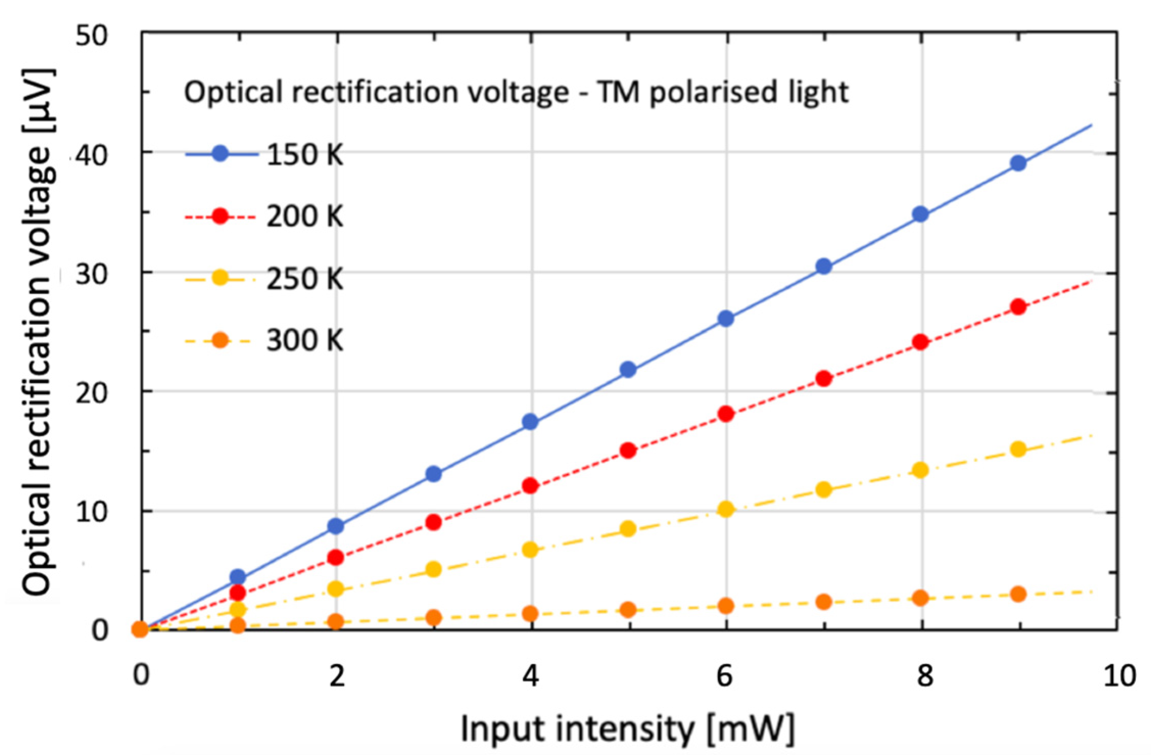
After this rather numerical analysis, the question remains how the proposed device will be configured in detail. As outlined, for instance in [
17], the polarization selection rule normally prevents any ISB-interaction between vertically incoming light and horizontally oriented QWs. Therefore, an optical diffraction grating to reorient the light into the horizontal direction is required. In
Figure 3, we present the measured optical rectification voltage as a function of light input intensity; thus, the typical responsivity characteristics of existing 1.55 µm ISB detectors. Another crucially important issue is the time response of such devices. The time response of the described detector can be estimated as follows: We first compare the frequency response of the proposed photo-transistor to the typical frequency response of an equivalent superlattice detector—like described in [
13]. From the frequency response, the rise and fall times can then be estimated via the following relation: τ
rise = τ
fall = 0.35/f
res. The detector from the previous publication is square-shaped with 200 µm side length; and is therefore roughly 800 times as large as the 2 × 25 µm
2 sized photo-transistor gate. More precisely, its metal surface is, therefore, 1600 times as large as the net (50%) metal coverage of the gate of this device. For our above cited, stand-alone detector, a 3 dB frequency of f
3dB = 250 MHz was seen. If this quantity is conservatively multiplied by the geometrical factor 400 from above, then we end up at a 3 dB frequency of f
3dB = 100 GHz and rise/fall times of 3.5 ps.
For a broad range of appropriately oriented optical input intensities—i.e., from vertically incident power levels between 0.1 mW and 10 mW and on a spot size of 60 µm diameter—a linear dependence of the measured electrical output voltage was observed [
11]. Based on these data, the general strategy of the presented optimizing procedure becomes evident: Although the responsivity characteristics of our ISB SL device reveals a clear photovoltaic behavior, its signal needs to be amplified to reach a practically useful level. And since the nitride materials are routinely used for the fabrication of multi-GHz HFET amplifiers, a monolithic integration of these two device functionalities (i.e., ‘ISB detector’ and ‘HFET amplifier’) will—without any doubt—result in a much higher overall detector performance.
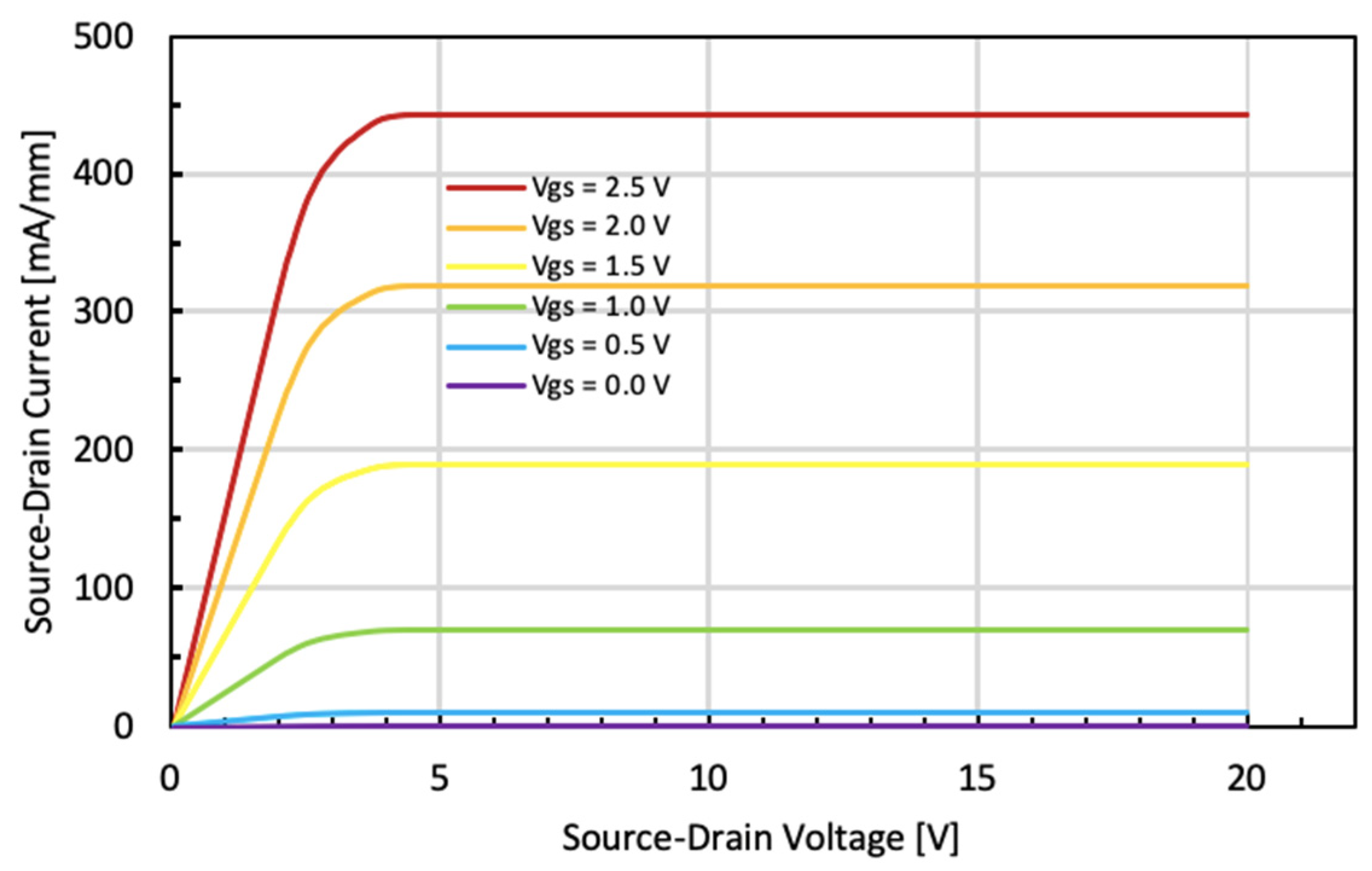
Figure 4 shows the simulated HFET characteristics based on reference [
16], but taking into account the present device with its considerably thicker channel layer than standard transistors. Compared to the best reported devices, it is obvious that a slightly lower performance level is expected.
How will such a monolithically integrated ISB-detector/HFET device be utilized in practical applications? Among the different possibilities, we envisage two different interesting cases. In the first type of applications, the device will serve as a sensitive detector for the near-infrared wavelength range around 1.55 µm. On the basis of such a device—configured as a one- or even a two-dimensional array—a very robust near-infrared camera with a lower detection limit of 10 µW per pixel can be built. However, an even more appealing application is given by the high-frequency capability of a stand-alone detector. Since no p-n-junction is present in this device, no space charge region and, therefore, no parasitic capacitance will build up under operation. For this reason, the frequency limit of the proposed device will be much higher than the one of classical p-n-junction photo-detectors. Based on our numerical simulations, we expect that the corner frequency of an appropriately small device will reach values in excess of 100 GHz. Together with the high chemical, thermal, and mechanical robustness of this detector, this is very interesting for optical telecommunication applications under harsh environmental conditions.
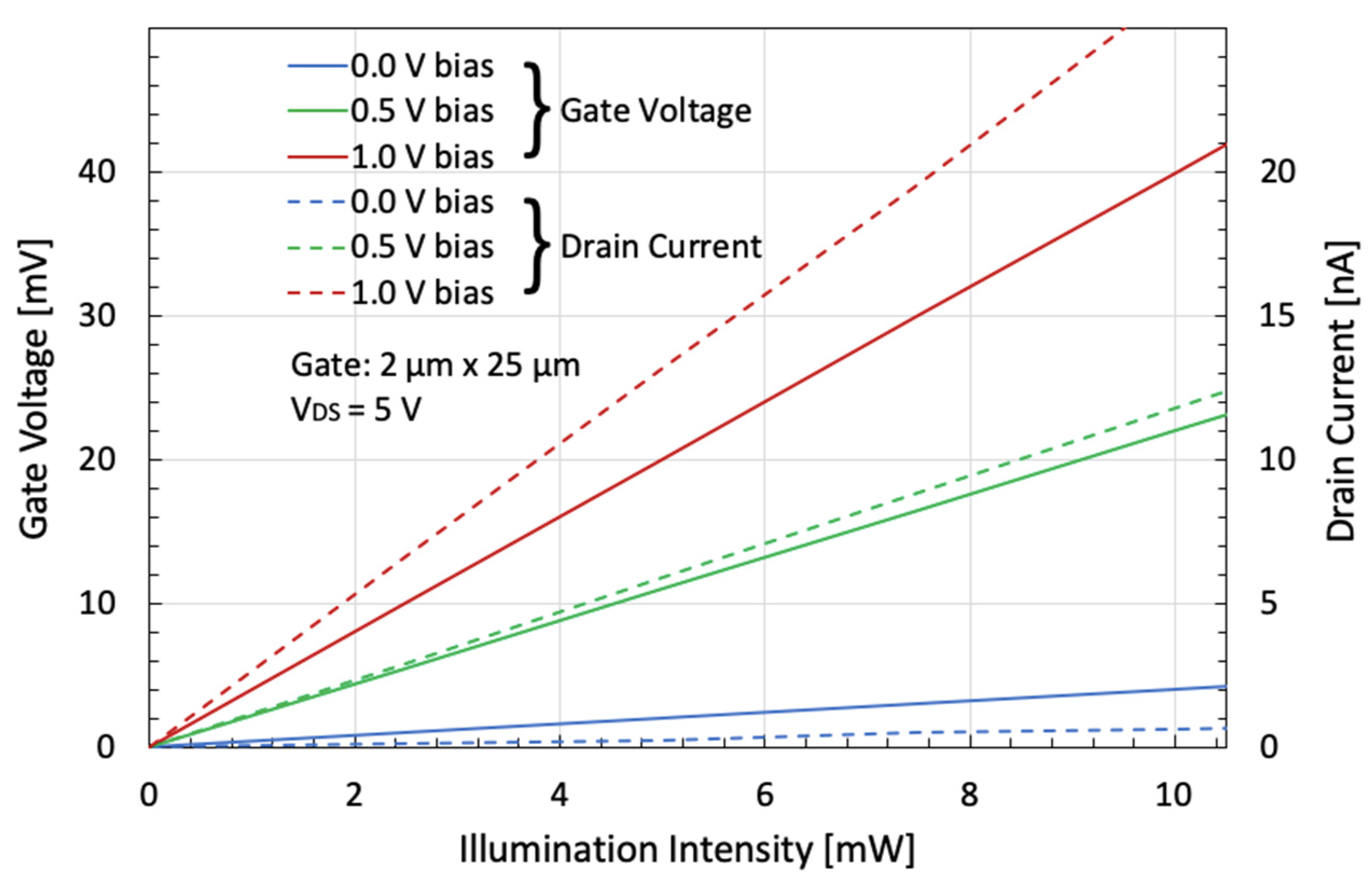
Therefore, we present, in
Figure 5, gate voltage and drain current vs. illumination intensity of this photo-transistor. Three different constant bias voltages of V
gs,el = 0.0, 0.5, and 1.0 V were applied. As expected from its maximal transconductance value, the application of V
gs,el = 1 V results in the highest signal.
Such GaN-based photo-transistors lend themselves also for a potential use as an optically logic gate under harsh environmental conditions. They could be combined suitably to form either a logic AND or NAND or an OR or NOR-gate. The input would be optical, while the output will become electrical. In the simplest configuration, an elongated transistor with two parallel gates can be imagined. This example would correspond to a logic AND-gate: The transistor will switch only if both gates are illuminated and enable current flow from source to drain.
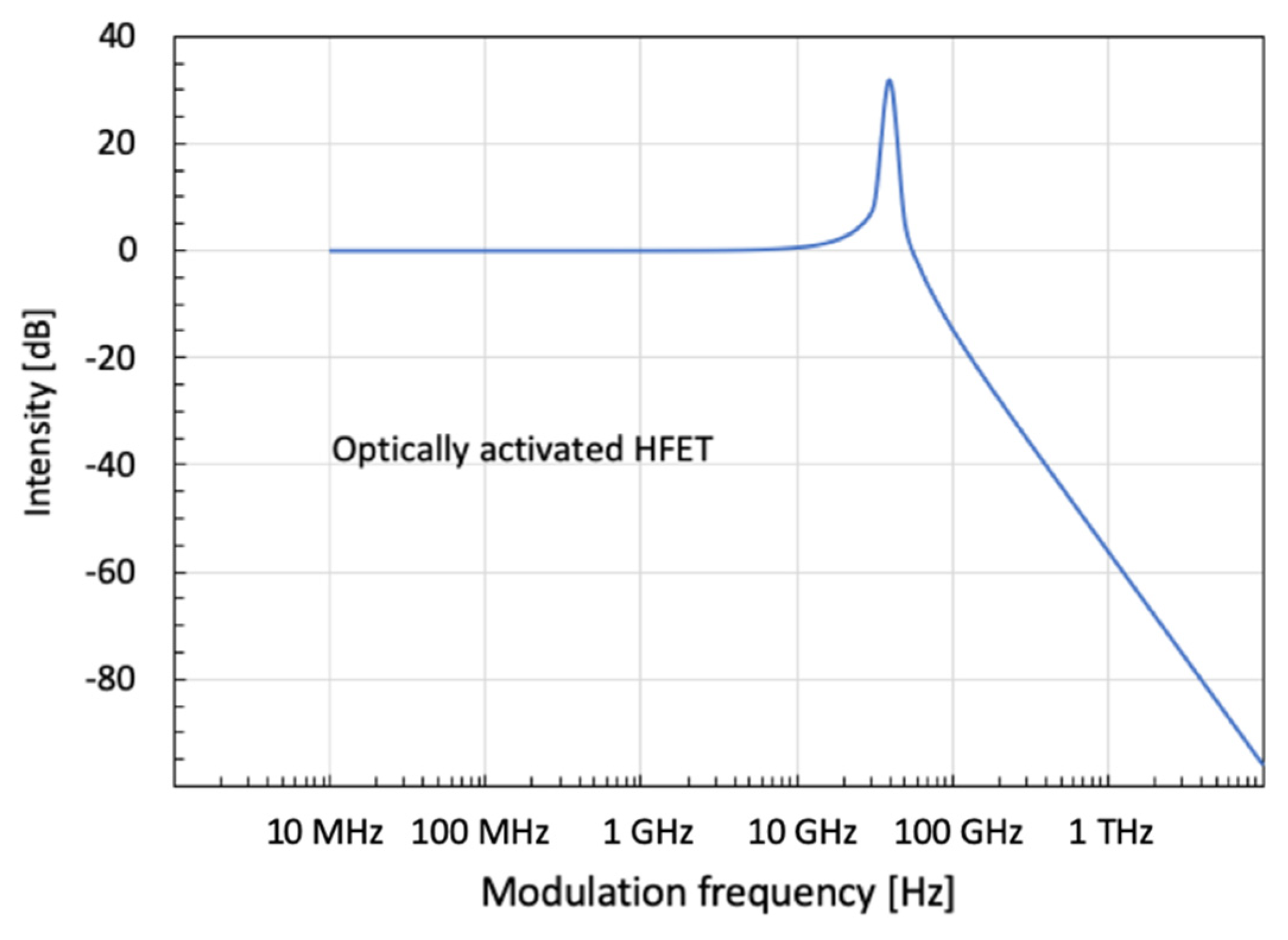
In
Figure 6, we finally show the simulated high frequency behavior of this HFET-amplified AlN/GaN-SL-detector. The signal gets maximal at nearly 80 GHz and—with a slightly reduced intensity—reaches frequencies around 100 GHz. Even higher bandwidth limits are expected from a careful process optimization.
5. Conclusions
A GaN/AlN-based, highly sensitive, and very fast photo-transistor for 1.55 µm is proposed. The device consists of a 100-period SL detector with 1.5 nm GaN QWs and 15 nm AlN barrier layers, which will be used as gate region of an AlGaN-based HFET. Based on measured characteristics of a standard GaN/AlN SL detector, numerical simulations of the final device predict a marked performance improvement. Our simulations suggest for this device a frequency limit approaching 100 GHz.


