
Simulation and Analysis of Microring Electric Field Sensor Based on a Lithium Niobate-on-Insulator

 ,
, 
Abstract
:1. Introduction
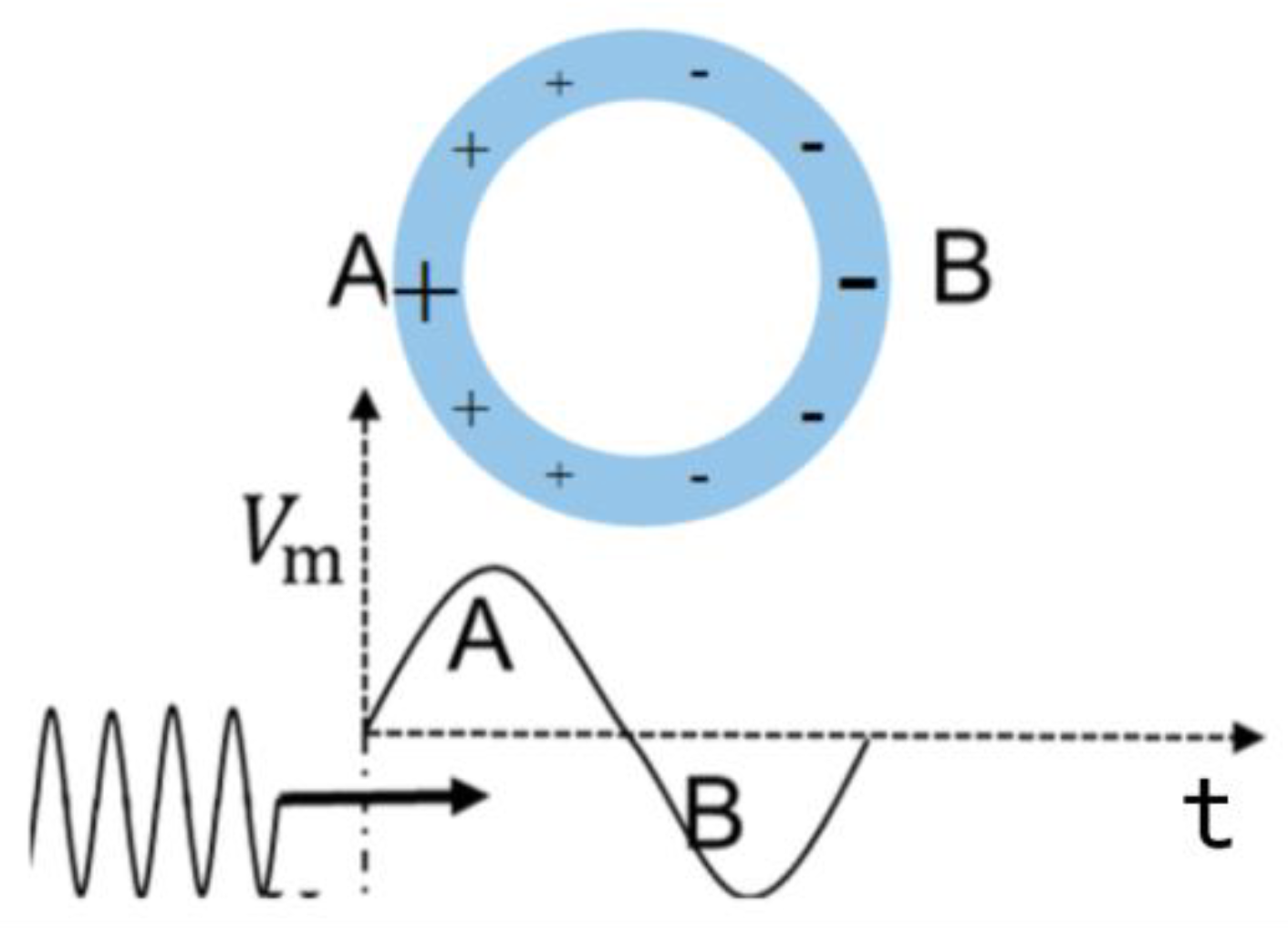
2. Structure
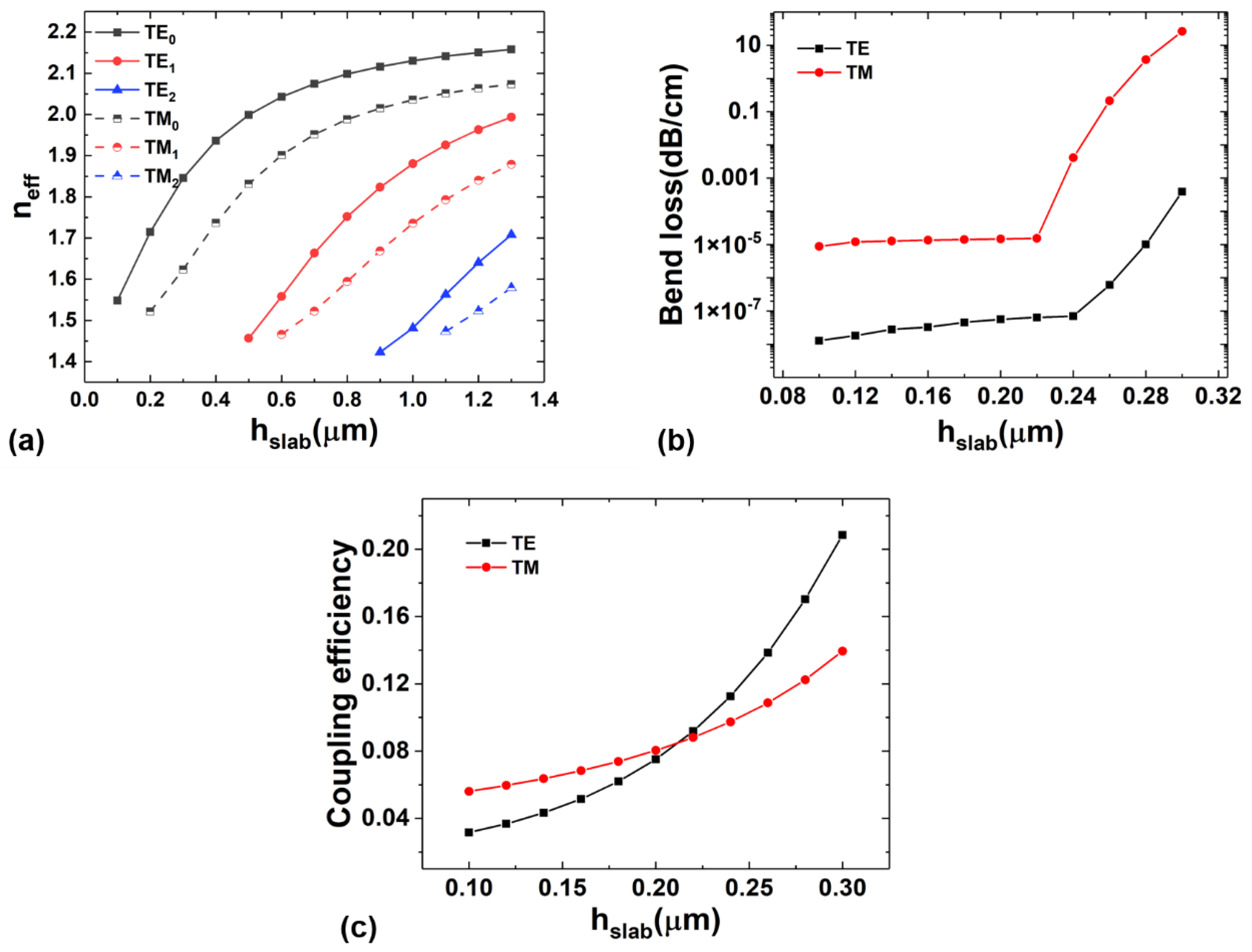
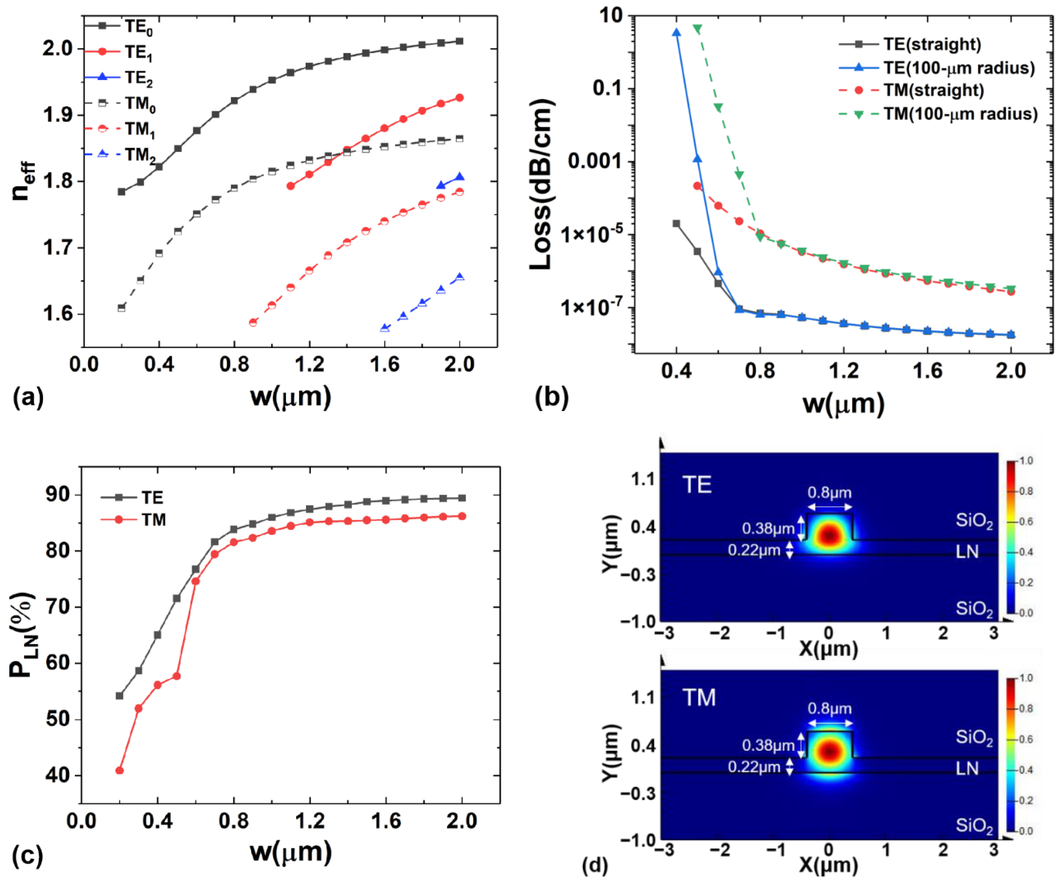
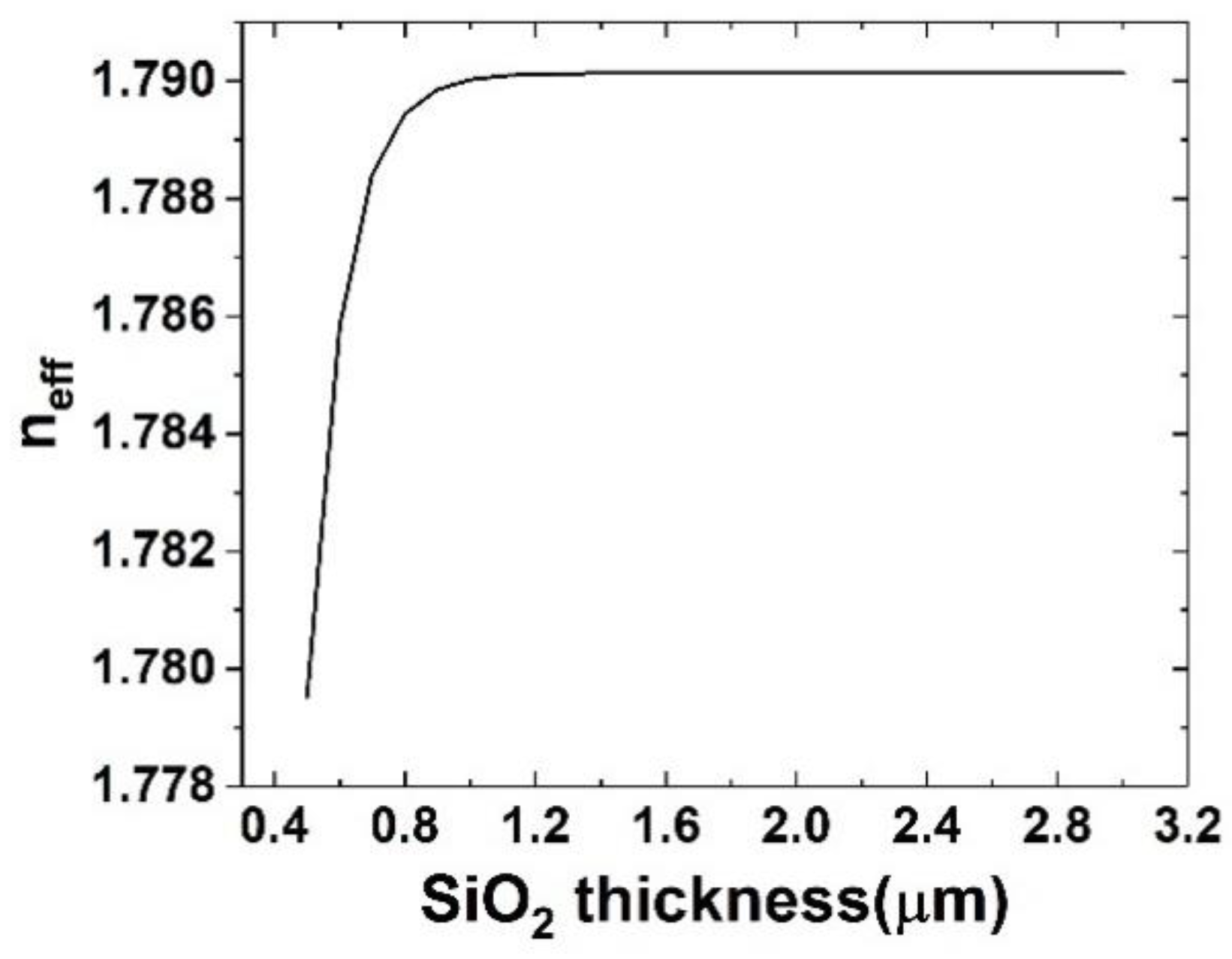
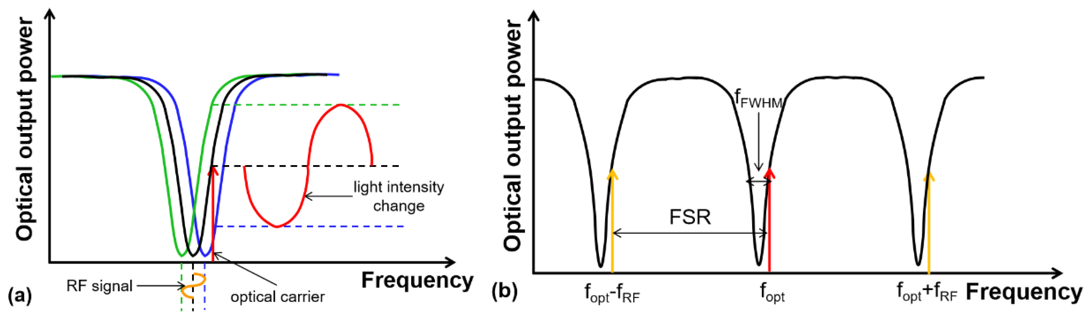
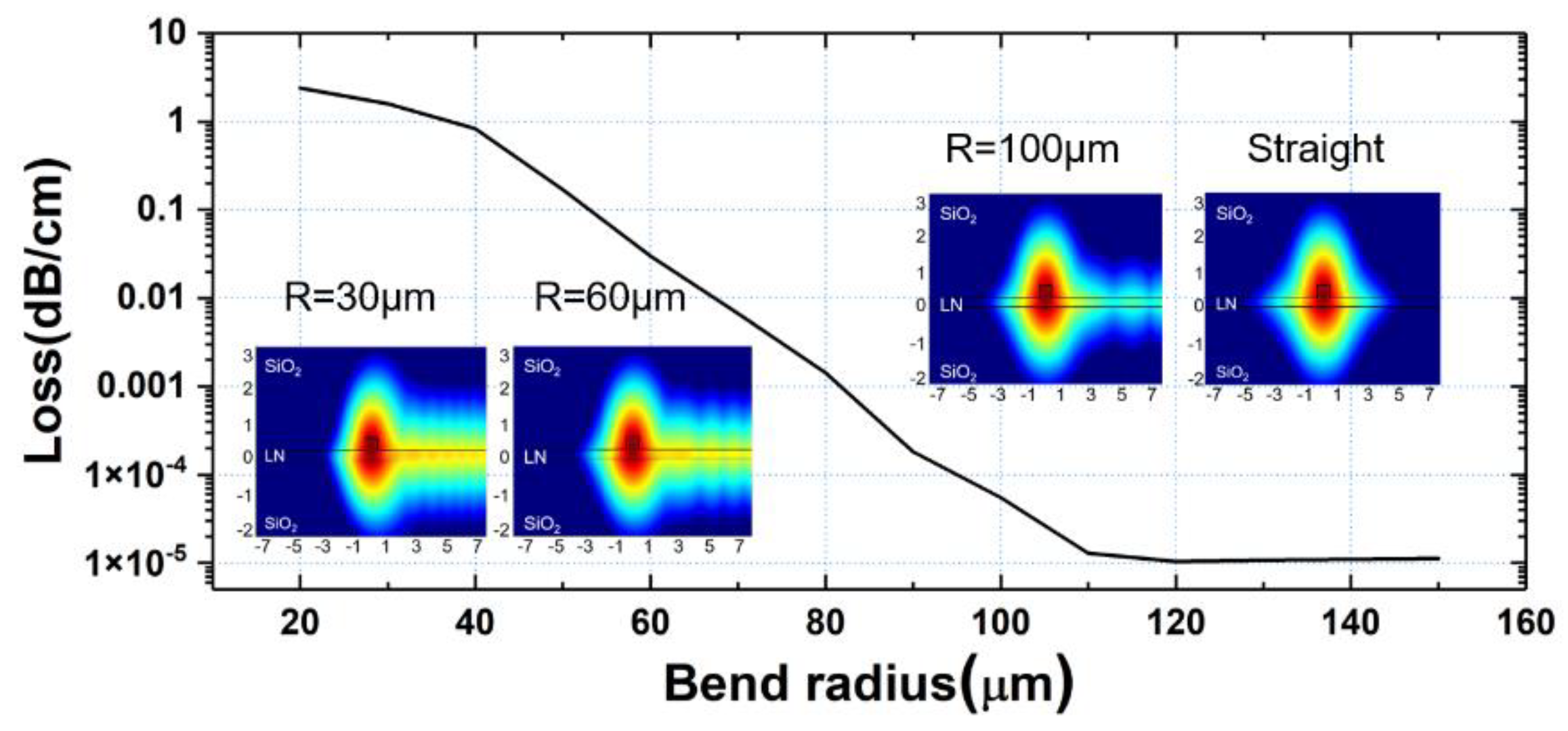
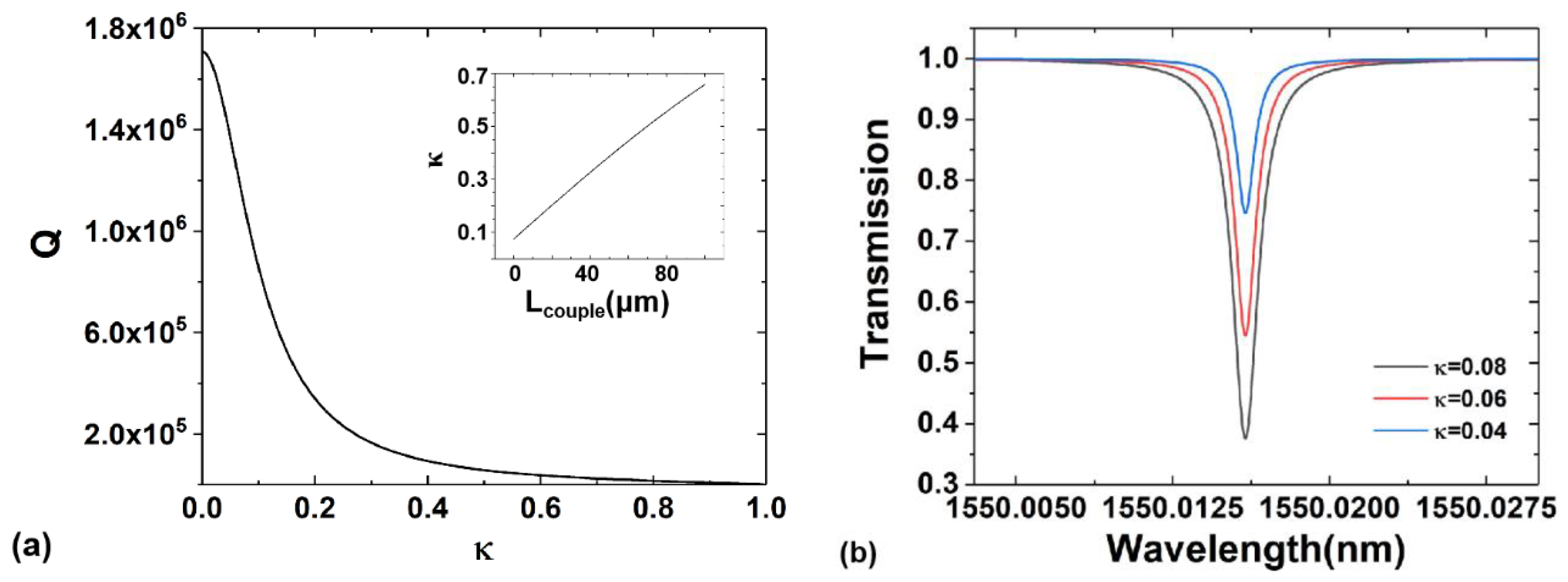
3. Results and Discussion
4. Conclusions
Author Contributions
Funding
Institutional Review Board Statement
Informed Consent Statement
Data Availability Statement
Acknowledgments
Conflicts of Interest
References
- Rabiei, P.; Steier, W.H.; Zhang, C.; Dalton, L.R. Polymer micro-ring filters and modulators. J. Light. Technol. 2002, 20, 1968–1975. [Google Scholar] [CrossRef]
- Hryniewicz, J.V.; Absil, P.P.; Little, B.E.; Wilson, R.A.; Ho, P.T. Higher order filter response in coupled microring resonators. IEEE Photonics Technol. Lett. 2000, 12, 320–322. [Google Scholar] [CrossRef]
- Chen, L.; Reano, R.M. Compact electric field sensors based on indirect bonding of lithium niobate to silicon microrings. Opt. Express 2012, 20, 4032–4038. [Google Scholar] [CrossRef]
- Huang, M.; Yang, J.; Jun, S.; Mu, S.; Lan, Y. Simulation and Analysis of a Metamaterial Sensor Based on a Microring Resonator. Sensors 2011, 11, 5886–5899. [Google Scholar] [CrossRef] [Green Version]
- Zhou, L.; Sun, X.; Li, X.; Chen, J. Miniature Microring Resonator Sensor Based on a Hybrid Plasmonic Waveguide. Sensors 2011, 11, 6856–6867. [Google Scholar] [CrossRef] [Green Version]
- Wan, L.; Chandrahalim, H.; Chen, C.; Chen, Q.S.; Mei, T.; Oki, Y.; Nishimura, N.; Guo, L.J.; Fan, X.D. On-chip, high-sensitivity temperature sensors based on dye-doped solid-state polymer microring lasers. Appl. Phys. Lett. 2017, 111, 061109. [Google Scholar] [CrossRef]
- Tazawa, H.; Kuo, Y.H.; Dunayevskiy, I.; Luo, J.D.; Jen, A.K.Y.; Fetterman, H.R.; Steier, W.H. Ring resonator-based electrooptic polymer traveling-wave modulator. J. Light. Technol. 2006, 24, 3514–3519. [Google Scholar] [CrossRef]
- Wang, C.; Zhang, M.; Stern, B.; Lipson, M.; Loncar, M. Nanophotonic lithium niobate electro-optic modulators. Opt. Express 2018, 26, 1547–1555. [Google Scholar] [CrossRef] [Green Version]
- Chen, L.; Wood, M.G.; Reano, R.M. 12.5 pm/V hybrid silicon and lithium niobate optical microring resonator with integrated electrodes. Opt. Express 2013, 21, 27003–27010. [Google Scholar] [CrossRef]
- Guarino, A.; Poberaj, G.; Rezzonico, D.; Degl’Innocenti, R.; Gunter, P. Electro-optically tunable microring resonators in lithium niobate. Nat. Photonics 2007, 1, 407–410. [Google Scholar] [CrossRef]
- Zhang, M.; Buscaino, B.; Wang, C.; Shams-Ansari, A.; Reimer, C.; Zhu, R.R.; Kahn, J.M.; Loncar, M. Broadband electro-optic frequency comb generation in a lithium niobate microring resonator. Nature 2019, 568, 373–377. [Google Scholar] [CrossRef]
- Stern, B.; Ji, X.C.; Okawachi, Y.; Gaeta, A.L.; Lipson, M. Battery-operated integrated frequency comb generator. Nature 2018, 562, 401–405. [Google Scholar] [CrossRef] [PubMed] [Green Version]
- Bogaerts, W.; De Heyn, P.; Van Vaerenbergh, T.; De Vos, K.; Selvaraja, S.K.; Claes, T.; Dumon, P.; Bienstman, P.; Van Thourhout, D.; Baets, R. Silicon microring resonators. Laser Photonics Rev. 2012, 6, 47–73. [Google Scholar] [CrossRef]
- Liu, M.; Yin, X.B.; Ulin-Avila, E.; Geng, B.S.; Zentgraf, T.; Ju, L.; Wang, F.; Zhang, X. A graphene-based broadband optical modulator. Nature 2011, 474, 64–67. [Google Scholar] [CrossRef] [PubMed]
- Novoselov, K.S.; Fal’ko, V.I.; Colombo, L.; Gellert, P.R.; Schwab, M.G.; Kim, K. A roadmap for graphene. Nature 2012, 490, 192–200. [Google Scholar] [CrossRef] [PubMed]
- Xu, Q.F.; Schmidt, B.; Pradhan, S.; Lipson, M. Micrometre-scale silicon electro-optic modulator. Nature 2005, 435, 325–327. [Google Scholar] [CrossRef] [PubMed]
- Zhang, C.; Morton, P.A.; Khurgin, J.B.; Peters, J.D.; Bowers, J.E. Ultralinear heterogeneously integrated ring-assisted Mach-Zehnder interferometer modulator on silicon. Optica 2016, 3, 1483–1488. [Google Scholar] [CrossRef]
- Timurdogan, E.; Sorace-Agaskar, C.M.; Sun, J.; Hosseini, E.S.; Biberman, A.; Watts, M.R. An ultralow power athermal silicon modulator. Nat. Commun. 2014, 5, 4008. [Google Scholar] [CrossRef] [PubMed] [Green Version]
- Aoki, M.; Suzuki, M.; Sano, H.; Kawano, T.; Ido, T.; Taniwatari, T.; Uomi, K.; Takai, A. Ingaas/Ingaasp Mqw Electroabsorption Modulator Integrated with a dfb Laser Fabricated by Band-Gap Energy Control Selective-Area Mocvd. IEEE J. Quantum Electron. 1993, 29, 2088–2096. [Google Scholar] [CrossRef]
- Lee, M.; Katz, H.E.; Erben, C.; Gill, D.M.; Gopalan, P.; Heber, J.D.; McGee, D.J. Broadband modulation of light by using an electro-optic polymer. Science 2002, 298, 1401–1403. [Google Scholar] [CrossRef] [PubMed]
- Ahmed, A.N.R.; Shi, S.Y.; Zablocki, M.; Yao, P.; Prather, D.W. Tunable hybrid silicon nitride and thin-film lithium niobate electro-optic microresonator. Opt. Lett. 2019, 44, 618–621. [Google Scholar] [CrossRef] [Green Version]
- Boes, A.; Corcoran, B.; Chang, L.; Bowers, J.; Mitchell, A. Status and Potential of Lithium Niobate on Insulator (LNOI) for Photonic Integrated Circuits. Laser Photonics Rev. 2018, 12, 1700256. [Google Scholar] [CrossRef]
- Bahadori, M.; Yang, Y.S.; Goddard, L.L.; Gong, S.B. High performance fully etched isotropic microring resonators in thin-film lithium niobate on insulator platform. Opt. Express 2019, 27, 22025–22039. [Google Scholar] [CrossRef] [Green Version]
- Zhang, M.; Wang, C.; Cheng, R.; Shams-Ansari, A.; Loncar, M. Monolithic ultra-high-Q lithium niobate microring resonator. Optica 2017, 4, 1536–1537. [Google Scholar] [CrossRef]
- Cai, L.T.; Kong, R.R.; Wang, Y.W.; Hu, H. Channel waveguides and y-junctions in x-cut single-crystal lithium niobate thin film. Opt. Express 2015, 23, 29211–29221. [Google Scholar] [CrossRef]
- Wang, Y.W.; Chen, Z.H.; Cai, L.T.; Jiang, Y.P.; Zhu, H.B.; Hu, H. Amorphous silicon-lithium niobate thin film strip-loaded waveguides. Opt. Mater. Express 2017, 7, 4018–4028. [Google Scholar] [CrossRef]
- Jin, S.L.; Xu, L.T.; Zhang, H.H.; Li, Y.F. LiNbO3 Thin-Film Modulators Using Silicon Nitride Surface Ridge Waveguides. IEEE Photonics Technol. Lett. 2016, 28, 736–739. [Google Scholar] [CrossRef]
- Wu, R.B.; Wang, M.; Xu, J.; Qi, J.; Chu, W.; Fang, Z.W.; Zhang, J.H.; Zhou, J.X.; Qiao, L.L.; Chai, Z.F.; et al. Long Low-Loss-Litium Niobate on Insulator Waveguides with Sub-Nanometer Surface Roughness. Nanomaterials 2018, 8, 910. [Google Scholar] [CrossRef] [Green Version]
- Ayazi, A.; Hsu, R.C.J.; Houshmand, B.; Steier, W.H.; Jalali, B. All-dielectric photonic-assisted wireless receiver. Opt. Express 2008, 16, 1742–1747. [Google Scholar] [CrossRef] [PubMed]
- Hsu, R.C.J.; Ayazi, A.; Houshmand, B.; Jalali, B. All-dielectric photonic-assisted radio front-end technology. Nat. Photonics 2007, 1, 535–538. [Google Scholar] [CrossRef]
- Cohen, D.A.; Levi, A.F.J. Microphotonic components for a mm-wave receiver. Solid·State Electron. 2001, 45, 495–505. [Google Scholar] [CrossRef]
- Schlarb, U.; Betzler, K. A generalized sellmeier equation for the refractive indices of lithium niobate. Ferroelectrics 1994, 156, 99–104. [Google Scholar] [CrossRef]
- Jazbinsek, M.; Zgonik, M. Material tensor parameters of LiNbO3 relevant for electro- and elasto-optics. Appl. Phys. B Lasers Opt. 2002, 74, 407–414. [Google Scholar]
- Ilchenko, V.S.; Savchenkov, A.A.; Matsko, A.B.; Maleki, L. Whispering-gallery-mode electro-optic modulator and photonic microwave receiver. J. Opt. Soc. Am. B Opt. Phys. 2003, 20, 333–342. [Google Scholar] [CrossRef]
- Sun, Y.X.; Ji, W.; Yin, R.; Wu, C.H.; Gong, Z.S. The reconfigurable dispersion compensator based on LNOI waveguide grating. Opt. Quantum Electron. 2018, 50, 310. [Google Scholar] [CrossRef]
- Han, H.P.; Xiang, B.X.; Zhang, J.L. Simulation and Analysis of Single-Mode Microring Resonators in Lithium Niobate Thin Films. Crystals 2018, 8, 342. [Google Scholar] [CrossRef] [Green Version]
- Han, H.P.; Xiang, B.X. Simulation and analysis of electro-optic tunable microring resonators in silicon thin film on lithium niobate. Sci. Rep. 2019, 9, 6302. [Google Scholar] [CrossRef] [PubMed]


Publisher’s Note: MDPI stays neutral with regard to jurisdictional claims in published maps and institutional affiliations. |
© 2021 by the authors. Licensee MDPI, Basel, Switzerland. This article is an open access article distributed under the terms and conditions of the Creative Commons Attribution (CC BY) license (http://creativecommons.org/licenses/by/4.0/).
Share and Cite
Wu, Z.; Lin, Y.; Han, S.; Yin, X.; Ding, M.; Guo, L.; Yang, X.; Zhao, M. Simulation and Analysis of Microring Electric Field Sensor Based on a Lithium Niobate-on-Insulator. Crystals 2021, 11, 359. https://doi.org/10.3390/cryst11040359
Wu Z, Lin Y, Han S, Yin X, Ding M, Guo L, Yang X, Zhao M. Simulation and Analysis of Microring Electric Field Sensor Based on a Lithium Niobate-on-Insulator. Crystals. 2021; 11(4):359. https://doi.org/10.3390/cryst11040359
Chicago/Turabian StyleWu, Zhenlin, Yumeng Lin, Shaoshuai Han, Xiong Yin, Menghan Ding, Lei Guo, Xin Yang, and Mingshan Zhao. 2021. "Simulation and Analysis of Microring Electric Field Sensor Based on a Lithium Niobate-on-Insulator" Crystals 11, no. 4: 359. https://doi.org/10.3390/cryst11040359