Article

High Thermal Stability of κ-Ga2O3 Grown by MOCVD

Center for Quantum Devices, Department of Electrical and Computer Engineering, Northwestern University, Evanston, IL 60208, USA
*
Author to whom correspondence should be addressed.
Crystals 2021, 11(4), 446; https://doi.org/10.3390/cryst11040446
Submission received: 24 March 2021 / Revised: 18 April 2021 / Accepted: 18 April 2021 / Published: 20 April 2021
(This article belongs to the Special Issue Advanced Functional Oxide Ceramics)

Abstract

:
We report a high thermal stability of kappa gallium oxide grown on c-plane sapphire substrate by metal organic chemical vapor deposition. Kappa gallium oxide is widely known as a metastable polymorph transitioning its phase when subjected to a high temperature. Here, we show the kappa gallium oxide whose phase is stable in a high temperature annealing process at 1000 °C. These oxide films were grown at 690 °C under nitrogen carrier gas. The materials showed high electrical resistivity when doped with silicon, whereas the film conductivity was significantly improved when doped with both indium and silicon. This work provides a pathway to overcoming limitations for the advance in utilizing kappa gallium oxide possessing superior electrical characteristics.

1. Introduction

Gallium oxide (Ga2O3) has been regarded as a promising next-generation material for realizing future ultra-wide bandgap optoelectronics and/or electronics such as ultraviolet solar blind photodetectors (SBPD) or high-power transistors. Despite of its potential, a complicated nature of Ga2O3 requires further understanding in the structural and electronic properties to advance the application fields to the greater extend. Among five different polymorphic forms (α-, β-, γ-, δ-, and κ-) of Ga2O3, β-phase Ga2O3 has widely been studied, since it is the most thermally and chemically stable as compared to other structures [1,2]. Moreover, a recent development in fabricating single crystal β-Ga2O3 substrates has been boosting up the expectation for the realization of devices based on such material in near future [3]. Apart from this promising phase of Ga2O3, growing attention has also been given to the metastable phase of Ga2O3, which is widely known as ε- or κ-phase [4,5], since it exhibits similar properties with β-Ga2O3 such as a wide direct bandgap energy of approximately 4.8 eV. Furthermore, various alloys containing other elements such as magnesium, indium, and aluminum can be utilized to tune its bandgap within the ultraviolet C light (UVC) solar blind band (200–280 nm) [6,7,8]. More importantly, the κ-Ga2O3 has been reported to exhibit unique properties, ferroelectric behavior and large polarization, that other polymorphs do not possess [9,10]. For example, the κ-Ga2O3 is predicted to have a large spontaneous polarization value which is about three times larger than the one of aluminum nitride [9]. In spite of numerous advantages of κ-phase, little has been studied making use of κ-Ga2O3 in the application. This is mainly due to the fact that the κ-Ga2O3 transits its phase to the β-Ga2O3 if high temperature energy is applied in order to activate dopants and to decrease the defect density inside layers [2,3]. Thus, further advancement of employing κ-Ga2O3 cannot be made unless the phase transition at high temperature issue is solved. Herein, we report a high thermal stability of κ-Ga2O3 grown on c-plane sapphire substrate by metal organic chemical vapor deposition (MOCVD). The κ-Ga2O3 thin films can withstand a high temperature annealing process at 1000 °C without having a phase transition. Moreover, when the materials are doped with both silicon and indium, the improvement in electrical properties has been observed. This work provides a pathway to overcome limitations for the advance in utilizing kappa gallium oxide possessing superior electrical characteristics.

2. Materials and Methods

We grow various structures listed in Table 1 under N2 carrier gas using Trimethyl-gallium (TMGa), Trimethyl-indium (TMIn), pure H2O vapor and Silane (SiH4) as Ga, In, O and Si precursors, respectively. Ga2O3 growth was performed on c-plane sapphire substrates by AIXTRON AIX200/4 horizontal MOCVD reactor at the growth temperature of 690 °C and at the pressure of 50 mbar. The post thermal annealing process was carried out for 1 minute by either ex situ rapid thermal annealing (RTA) or in situ annealing within the MOCVD reactor [11]. The structural property and the corresponding phase of the as-grown and annealed Ga2O3 epilayers were investigated by high-resolution x-ray diffraction (HR-XRD). Field emission scanning electron microscopy (SEM), Hitachi S-4500, was utilized to analyze the surface morphology of samples and also to measure the thickness of respective Ga2O3 epilayers. Electrical characteristics, including resistivity, mobility, and carrier concentration, of the films were obtained by using Van der Pauw Hall technique at room temperature. Optical characterizations were performed by photoluminescence (PL) measurement using an Ar ion laser with excitation wavelength of 244 nm.

3. Results and Discussion

Figure 1 shows the XRD spectra of all the as-grown and annealed materials listed in Table 1. The corresponding phase of these as-grown epilayers is identified to be κ-phase (Figure 1a), aligning with the calculated (002), (004), and (006) planes, similar to the materials grown under H2 carrier gas as reported in our prior studies [11,12]. However, after the annealing process at 1000 °C, we did not observe any phase transition from κ- to β-phase. The phase of annealed epilayers remained the same, as shown in Figure 1b, which is opposed to the annealed Ga2O3 films grown under H2 [11]. This observation indicates a high thermal stability of κ-Ga2O3 epilayers grown under N2 carrier gas.
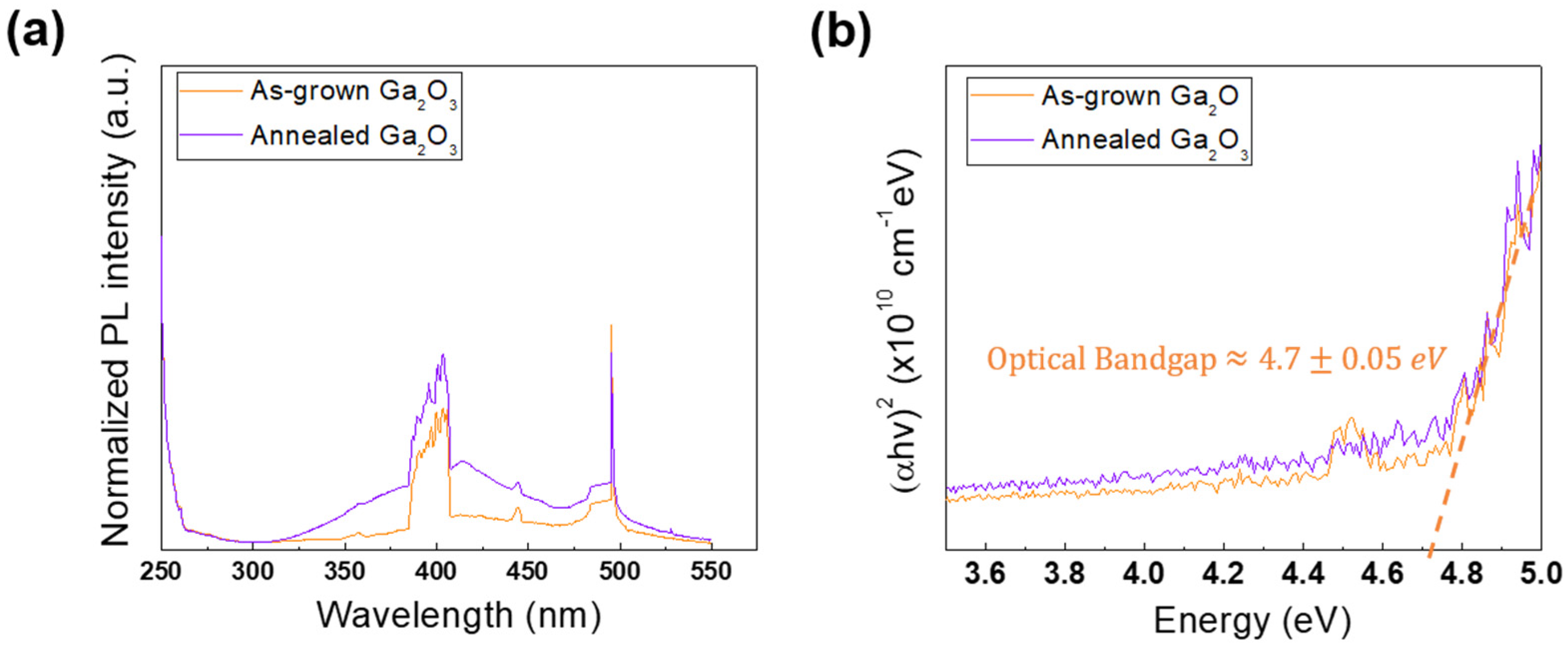
Normalized PL spectra were measured from all of the various as-grown and annealed Ga2O3 films in Table 1. As shown in Figure 2a, we could not observe any change in PL peaks as comparing between before and after annealing. However, in our previous papers [11,12], we demonstrated that the difference in PL peaks depending on its phase has been found, exhibiting that the peak of κ-Ga2O3 is around 420 nm, while the β-phase has a 360 nm PL peak. In addition to the PL spectrum, even in the optical bandgap measurement, the materials grown under N2 did not vary their optical bandgap upon annealing, which is in contrast to the materials grown under H2 ambience [12]. Both optical characterization techniques confirm that the phase of as-grown materials is κ-phase and this phase can be maintained even after annealing at 1000 °C, suggesting the thermal stable κ-Ga2O3 epilayers can be grown under N2 carrier gas.
Electrical characteristics of all epilayers listed in Table 1 are summarized in Table 2. The as-grown Ga2O3 layers without either silicon or indium dopant (Structure 1 and Structure 2) displayed extremely high resistivity, similar to the as-grown Ga2O3 grown under H2 carrier gas [12]. However, when materials were doped with silicon and the presence of TMIn during the growth (Structure 3), the hall mobility of the sample was remarkably improved. It exhibited an electron concentration (n ≈ 2 × 1017 cm−3) similar to that grown under H2, whereas the obtained hall electron mobility value was as low as around µ = 2 cm2V−1s−1. Regarding this phenomenon, we recently reported that the indium can play a role of a surfactant, causing the formation of less defective thin films, and thus resulting in the improvement in hall mobility [12]. On the other hand, contrary to our previous results, the annealing process did not induce an improvement of material conductivity. The Ga2O3 epilayers (Structure 1 and Structure 2) still presented a high resistivity while the co-doped Ga2O3 layer (Structure 3) had a slight increase in both carrier concentration (n ≈ 4 × 1018 cm−3) and hall mobility (µ = 4 cm2V−1s−1).
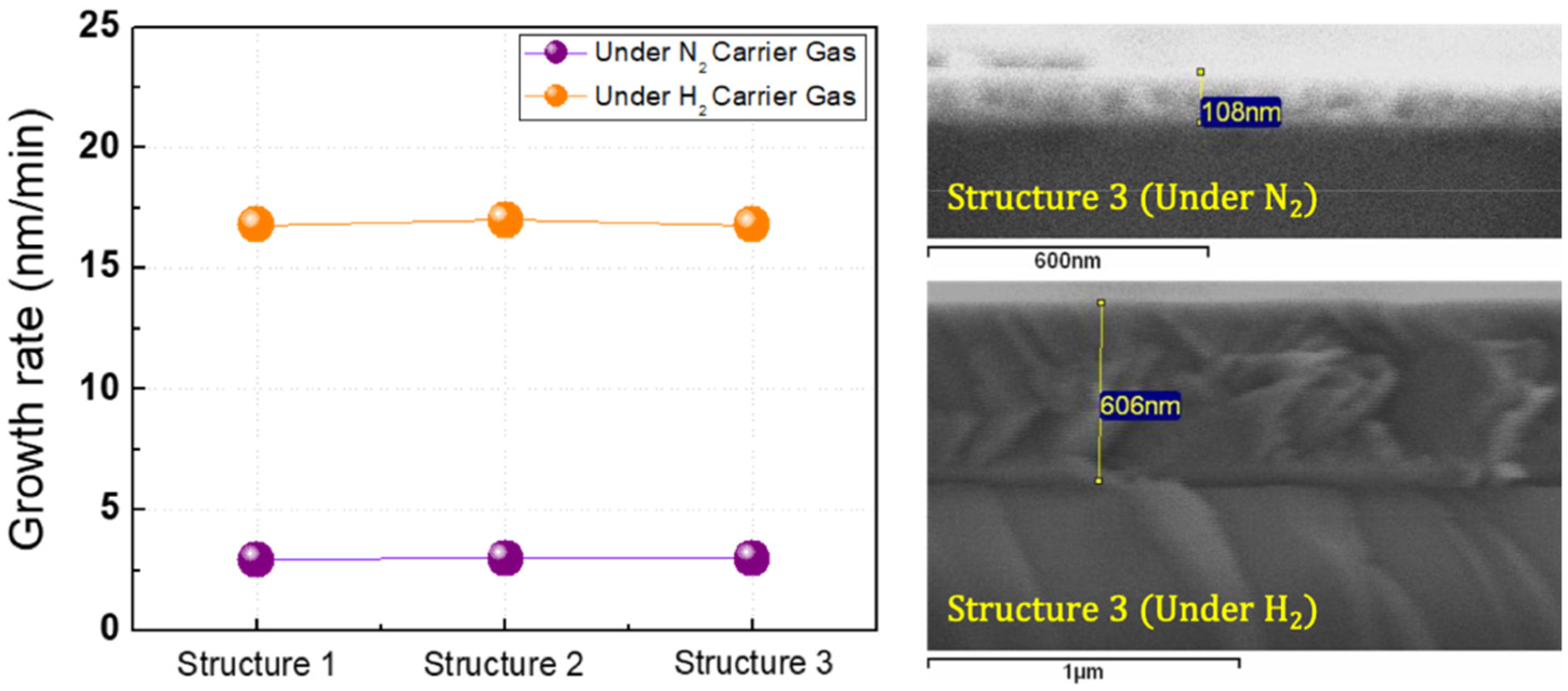
The thicknesses of the epilayers grown under different carrier gases were measured through the scanning electron microscope (SEM). The growth rates of respective epilayers under N2 carrier gas were around 3 nm/min regardless of structures (Figure 3), which is significantly lower than the layers grown under H2 carrier gas (17 nm/min) [11,12]. In case of structure 3, the film thickness was approximately 600 nm when it was deposited under H2. On the other hand, this was considerably reduced to 110 nm under N2 ambient. The decrease of the growth rate under N2 carrier gas can be interpreted as follows: according to the chemical reactions under either H2 or N2 carrier gas, the decomposition rate under N2 is much less efficient than under H2 carrier gas, leading to the low growth rate. This is also supported by the work [13], showing the TMGa is decomposed in different rates depending on the carrier gas. Due to the low decomposition speed, the undissolved organometallic complex would incorporate within epilayers giving the materials a high stable κ-phase. Furthermore, the incorporation of such organometallic complex makes the Si-doped materials compensated on the basis of the electrical properties displaying low carrier mobility and carrier concentration.

4. Conclusions

Highly thermal stable κ-Ga2O3 epilayers grown on c-plane sapphire substrate by MOCVD using N2 carrier gas were demonstrated through the various characterization techniques such as structural (XRD and SEM), optical (PL and transmission), and electrical (Hall measurement) measurement. Structural as well as optical characterization data have confirmed that the metastable κ-phase Ga2O3 can withstand its phase even when subjected to the annealing at 1000 °C, which is opposed to the case grown under H2 carrier gas where the phase transition occurred from κ- to β-phase. If the materials were grown with either silicon dopant or TMIn, both of the as-grown and annealed Ga2O3 films showed high resistive properties. However, the materials became conductive when doped with both silicon and indium. The growth rate under N2 carrier gas was significantly decreased as compared to those grown under H2, which can be attributed to different TMGa decomposition rates depending on the carrier gas. Despite the reduced growth rate, this observation suggests a pathway to maintain metastable κ-Ga2O3 possessing tremendous potential for further exploitation in the semiconductor industry.

Author Contributions

J.L. grew and characterized the materials and wrote the paper. H.K. helped with the X-ray measurement, and L.G. did the transmission measurement. M.R. provided the idea and supervised the whole research. All authors have read and agreed to the published version of the manuscript.

Funding

This work is supported by Air Force under agreement of FA9550-19-1-0410.

Institutional Review Board Statement

Not applicable.

Informed Consent Statement

Not applicable.

Data Availability Statement

The data presented in this study are available on request from the corresponding author.

Acknowledgments

This work is supported by Air Force under agreement of FA9550-19-1-0410. The authors would like to acknowledge the support and interest of Ali Sayir of USAF-AFMC AFMCAFOSR/RTB).

Conflicts of Interest

The authors declare no conflict of interest.

References

  1. Roy, R.; Hill, V.G.; Osborn, E.F. Polymorphism of Ga2O3 and the System Ga2O3—H2O. J. Am. Chem. Soc. 1952, 74, 719–722. [Google Scholar] [CrossRef]
  2. Razeghi, M.; Park, J.H.; McClintock, R.; Pavlidis, D.; Teherani, F.H.; Rogers, D.J.; Magill, B.A.; Khodaparast, G.A.; Xu, Y.; Wu, J.; et al. A Review of the Growth, Doping, and Applications of β-Ga2O3 Thin Films. Proc. SPIE 2018, 10533, 105330R1-24. [Google Scholar]
  3. Zhou, H.; Zhang, J.; Zhang, C.; Feng, Q.; Zhao, S.; Ma, P.; Hao, Y. A review of the most recent progresses of state-of-art gallium oxide power devices. J. Semicond. 2019, 40, 011803. [Google Scholar] [CrossRef]
  4. Cora, I.; Mezzadri, F.; Boschi, F.; Bosi, M.; Čaplovičová, M.; Calestani, G.; Dódony, I.; Pécz, B.; Fornari, R. The real structure of ε-Ga2O3 and its relation to κ-phase. CrystEngComm 2017, 19, 1509–1516. [Google Scholar] [CrossRef] [Green Version]
  5. Nikolaev, V.; Stepanov, S.; Pechnikov, A.V.; Shapenkov, S.; Scheglov, M.; Chikiryaka, A.; Vyvenko, O.F. HVPE Growth and Characterization of ε-Ga2O3 Films on Various Substrates. ECS J. Solid State Sci. Technol. 2020, 9, 045014. [Google Scholar] [CrossRef]
  6. Anhar Uddin Bhuiyan, A.F.M.; Feng, Z.; Johnson, J.M.; Huang, H.L.; Hwang, J.; Zhao, H. MOCVD Epitaxy of ultrawide bandgap β-(AlxGa1−x)2O3 with high-Al composition on (100) β-Ga2O3 substrates. Cryst. Growth Des. 2020, 20, 6722–6730. [Google Scholar] [CrossRef]
  7. Hatipoglu, I.; Mukhopadhyay, P.; Alema, F.; Sakthivel, T.S.; Seal, S.; Osinsky, A.; Schoenfeld, W.V. Tuning the responsivity of monoclinic solar-blind photodetectors grown by metal organic chemical vapor deposition. J. Phys. D Appl. Phys. 2020, 53, 454001. [Google Scholar] [CrossRef]
  8. Bi, X.; Wu, Z.; Huang, Y.; Tang, W. Stabilization and enhanced energy gap by Mg doping in ε-phase Ga2O3 thin films. AIP Adv. 2018, 8, 025008. [Google Scholar] [CrossRef] [Green Version]
  9. Maccioni, M.B.; Fiorentini, V. Phase diagram and polarization of stable phases of (Ga1−xInx)2O3. Appl. Phys. Express 2016, 9, 041102. [Google Scholar] [CrossRef] [Green Version]
  10. Nishinaka, H.; Miyauchi, N.; Tahara, D.; Morimoto, S.; Yoshimoto, M. Incorporation of indium into ε-gallium oxide epitaxial thin films grown via mist chemical vapour deposition for bandgap engineering. CrystEngComm 2018, 20, 1882–1888. [Google Scholar] [CrossRef]
  11. Lee, J.; Kim, H.; Gautam, L.; He, K.; Hu, X.; Dravid, V.; Razeghi, M. Study of Phase Transition in MOCVD Grown Ga2O3 from κ to β Phase by Ex Situ and In Situ Annealing. Photonics 2021, 8, 17. [Google Scholar] [CrossRef]
  12. Lee, J.; Kim, H.; Gautam, L.; Razeghi, M. Highly Conductive Co-Doped Ga2O3:Si-In Grown by MOCVD. Coatings 2021, 11, 287. [Google Scholar] [CrossRef]
  13. Chen, Q.; Dapkus, P.D. On the Thermal Decomposition of Trimethylgallium—A Molecular Beam Sampling Mass Spectroscopy Study. J. Electrochem. Soc. 1991, 138, 2821. [Google Scholar] [CrossRef]
Figure 1. (a) XRD patterns from the various (a) as-grown Ga2O3 layers and (b) the annealed samples listed in Table 1.
Crystals 11 00446 g001
Figure 2. (a) Photoluminescence spectra from representative value of the as-grown and annealed Ga2O3 layers. (b) Transmission measurement data of as-grown and annealed Ga2O3 thin films.
Crystals 11 00446 g002
Figure 3. Growth rate variation for different structures and the corresponding SEM images of structure 3.
Crystals 11 00446 g003
Table 1. Detail information about various growth structures. Nitrogen was used as a carrier gas during the growth.
StructureComponentsTMGaTMInH2OSiH4
Structure 1Ga2O3 [Reference]5 sccm (N2)0 sccm (N2)1600 sccm (N2)20 sccm (N2)
Structure 2Superlattice
[Ga2O3 (30 s)/In2O3 (1 min)]
5 sccm (N2)70 sccm (N2)1600 sccm (N2)0
Structure 3Superlattice
[Ga2O3 (30 s)/In2O3 (1 min)]
5 sccm (N2)70 sccm (N2)1600 sccm (N2)20 sccm (N2)
Table 2. Summary of the hall measurement data for the epitaxial layers listed in Table 1.
Before Annealing After Annealing
Hall MobilityCarrier ConcentrationHall MobilityCarrier Concentration
Structure 1Highly resistiveHighly resistiveHighly resistiveHighly resistive
Structure 2Highly resistiveHighly resistiveHighly resistiveHighly resistive
Structure 32 cm2/V·s2 × 1017 cm−34 cm2/V·s4 × 1018 cm−3
Publisher’s Note: MDPI stays neutral with regard to jurisdictional claims in published maps and institutional affiliations.