Article

Growth of SrB4O7 Crystal Fibers along the c-Axis by Micro-Pulling-Down Method

Graduate School of Science and Engineering, Yamaguchi University, Yamaguchi 753-8511, Japan
*
Author to whom correspondence should be addressed.
Crystals 2021, 11(8), 987; https://doi.org/10.3390/cryst11080987
Submission received: 10 July 2021 / Revised: 13 August 2021 / Accepted: 18 August 2021 / Published: 20 August 2021
(This article belongs to the Special Issue New Trends in Growth Technique of Micro-Pulling-Down Method)

Abstract

:
SrB4O7 (SBO) receives much attention as solid-state ultraviolet lasers for micro-machining, photochemical synthesis, and laser spectroscopy. For the application of SBO, the SBO crystals require the control of twinning to amplify the conversion light. We also expected that the inhibitation of the SrB2O4 appearance was essential. Here, we show the growth of SBO crystals along the c-axis through the micro-pulling-down method while alternating the application of electric fields (E). Without the application, single crystals were grown. At E ≧ 400 V/cm no needle domains of SrB2O4 inside SBO crystals existed; however, composition planes were formed and twin boundaries did not appear. In contrast, the inversion of surface morphology emerged, and the convex size was especially large at 1000 V/cm. These results demonstrate that convection is generated perpendicular to the growth front by alternating the application of electric fields. This surface morphological change contradicts the conventional concept of growth through the micro-pulling-down method. The distance from seed crystals vs. grain density plot also showed that the density did not decrease with a sufficient slope. Consequently, we concluded that the selection of the c-axis as growth faces is not fruitful to fabricate twins, and the selection of the growth condition, under which geometrical selection strongly affects, is the key.

1. Introduction

SrB4O7 (SBO) belongs to an orthorhombic structure with the space group of Pmn21 (a = 4.4273 Å, b = 10.714 Å, c = 4.2359 Å) [1,2]. SBO crystals also show high nonlinearity [3,4,5,6,7] and are transparent down to the deepest ultraviolet wavelength (125 nm) [4,5,6,7,8,9]. Hence, SBO receives much attention as solid-state ultraviolet lasers for semiconductor photolithography, micro-machining, photochemical synthesis, laser spectroscopy, and photoemission spectroscopy.
For the application of SBO, the SBO crystals require the appearance of the periodic twin structure, which is so-called quasi-phase-matching (QPM) structures. The QPM is the structure in which the sign of the nonlinear optical coefficient is periodically reversed and enabled to compensate the phase shift of the second harmonic generation [10,11]. Hence, the conversion light is, generally, amplified owing to the QPM structure. It is well-known that QPM structures in ferroelectric oxide materials can be formed by the application of an external electric field such as the poling method [10,12,13,14,15] and hot-pressing method [16]. However, since borates are non-ferroelectric crystals, with the utilization of the poling method and the hot-pressing method it is difficult to control twin boundary orientation.
Aleksandrovsky et al., for the first time, reported twinned structures of SBO crystals [17,18]. They succeeded in growing partially twinned SBO crystals by the Czochralski method (CZ). We expect that to control the formation of twin boundaries, the active incorporation of defects is further required by combining the growth under high temperature gradient G with the periodic application of electric fields. The growth by the micro-pulling-down method (μ-PD method) can be a suitable method. The orientation of the ions in the melt and the dipoles in the crystals can be controlled by alternating the application of electric fields. The temperature gradient range of the μ-PD method is 1–2 units larger than that of the CZ method because of the small hot zone [19,20,21], and electric fields can be applied homogeneously. The incorporation of homogenous composition in crystals is also possible owing to a high temperature gradient. Actually, in the case of the ferroelectric LiNbO3 (LN), Uda et al. succeeded in the domain inversion by applying an external electric current during the growth through the μ-PD method [22].
Recently, we tried to grow twinned SBO crystals along the b-axis during the application of electric fields by the μ-PD method [23]. Then, our previous study explored that the growth of SBO by the μ-PD method via alternating the application of opposing electric fields (E) exhibits two mechanisms. At E ≧ 400 V/cm needles of SrB2O4 appeared inside SBO fibers. At E≧ 1000 V/cm, new domains of SBO grew from the seed crystals, and growth twins were, interestingly, formed perpendicular to growth fronts. The twin face was (100) face. Thus, we revealed new challenges that the twin boundary is formed perpendicular to the growth front. Furthermore, we found the inversion of surface shapes during the growth even by the μ-PD method. We can explain the relationship between the two mechanisms and the inversion of surface shapes, using the concept of convection.
We expect that the inhibitation of the SrB2O4 appearance by the convection is the key for the fabrication of twins. Furthermore, the growth conditions, under which defects are further incorporated, are necessary for the formation of twins, as described so far. The orientation of the growth face is crucial for the fabrication of twins as well. Here we show the growth of SBO crystal fibers along the c-axis by the μ-PD method.

2. Materials and Methods

The μ-PD furnace used in this study was the same as in our previous studies [23,24,25,26]. 
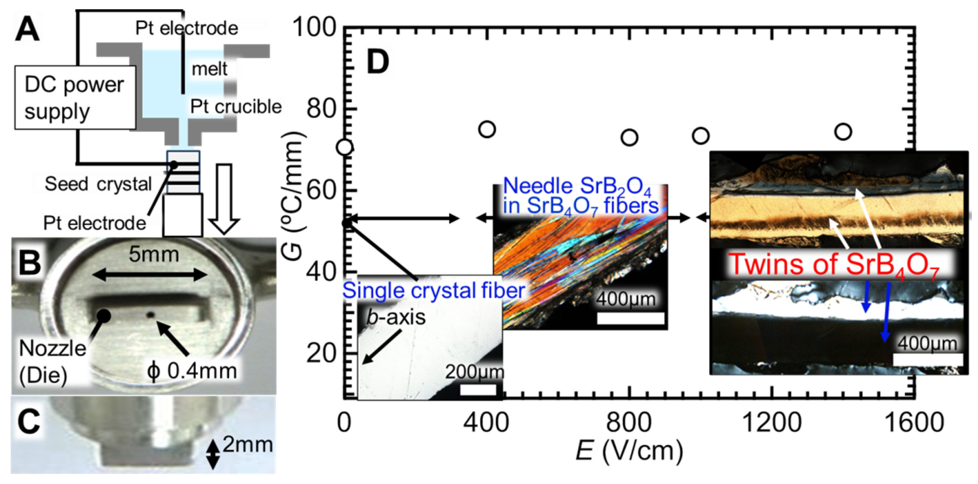
Figure 1A–C show a hot zone of the μ-PD furnace. A platinum crucible with a rectangular nozzle (5 mm × 1 mm × 2 mm (height)), which has a 0.4 mm cylindrical hole at the center of the base, was used. To set a temperature gradient (G) in crystals, the platinum crucible was surrounded by the refractory [23]. SBO ceramic powders with stoichiometric composition were prepared, and the raw material was melted in the platinum crucible by applying DC power. The temperature near the bottom of a nozzle remained at 1050 °C during the growth. Afterheaters were not placed in the furnace to carry out a high temperature gradient. Then, Pt electrodes were immersed in the melt. The tip of the Pt electrodes was placed on ca. 5 mm from the bottom of the nozzle. Seed crystals were fixed on an aluminum rod by Pt wire. The orientation of the seed crystals was confirmed by X-ray diffraction, transmittance electron microscopy (TEM), and the selected area electron diffraction (SAED). Then, they were attached to the bottom of the platinum nozzle, and were pulled down in air along the c-axis.
Figure 1D shows the growth conditions. The photographs corresponded to the summary of our previous study, which grew at 50–55 K/mm [23]. At that time, the pulling-down direction was the b-axis. In this study, the G of 70–75 K/mm just below the nozzle, and larger than in our previous study [23] was selected. Before the growth, the temperature profile from the bottom of the nozzle along the pulling-down direction was confirmed by a thermocouple. Then, the temperature gradient of 0.5–1 mm away from the nozzle was determined by the linear approximation [25]. These values would correspond to the intrinsic temperature gradient in the crystals near the interface to understand the crystal growth.
A pulling-down rate was also 0.02 mm/min. During the growth, various voltages were applied to the seed crystals through Pt wires and Pt electrodes. During the growth, various voltages of E in the range of 0–1400 V/cm were applied to the growth fronts of seed crystals through Pt electrodes [23]. The external voltage was switched every 30 min through a power supply.
After the growth, the fiber crystals were fixed in resin, and test pieces were polished. Then the fibers were observed by polarized optical microscopy (BX51, Olympus, Japan). During the growth, photographs of the meniscus just below the die were taken by a camera (SZ-31MR, Olympus, Japan). To determine the crystal faces of the boundaries in the test pieces, the fibers were cut off. The cross sections of fiber crystals were also processed by focused ion beam (FIB) (JIB-4000, JEOL, Japan), and the orientation of domain boundaries in crystal fibers was evaluated by TEM and SAED. The TEM/SAED observation was carried out, using a JEOL JEM-2100 electron microscope at an acceleration voltage of 200 kV. The camera length was 80 cm. The thickness of the samples, which were obtained by FIB, was ca. 200 ± 20 nm. The sample widths were ca. 5 μm, and the samples almost had no gradient at the surface. The brightness and contrast of the images were adjusted, using a software (ImageJ) [27]. The reciprocal lattice was evaluated and the zone axes were finally obtained, using the ReciPro software which can calculate the relation between the orientation of the crystals and 2D diffraction patterns [28,29]. In addition, the schematic drawing of the crystal structures was illustrated by a software (VESTA) [30].

3. Results

Figure 2 shows the SBO crystal fibers grown without the application of electric fields. Although the crystal has rough surfaces, the sample was almost transparent. The test piece was observed under crossed Nicols, and symbols in Figure 2C correspond to the crystallographic orientation of the seed crystals. The crystal showed uniform polarized light. In addition, the boundary between the seed crystals and grown crystals did not exist. Hence, we confirmed that the orientation of seed crystals remained in the grown crystal. Since SBO is too hard and fragile, polishing the test piece was difficult. By polishing, the test piece received scratches, and there were cracks. Sometimes the samples also partially lacked. When the stage was rotated by 45°, the polarized light was uniformly extinguished. This result demonstrates that the sample is a single crystal.
In this study, we separated and considered the growth conditions into E < 1000 and 1000 ≦ E to understand the growth mechanism. Figure 3 shows SBO crystal fibers grown at 400 V/cm. The fibers were slightly opaque owing to rough surfaces. The alternating timing of electric fields corresponded to the increase in the radius of the fiber. At the tip of fibers, no change in the radius was observed since the electrode of the Pt wire became away from the growth front of the seed crystals. Just above the surface of the seed crystal, additional domains appeared and grew (Figure 3B). In contrast, needle domains of SrB2O4 did not appear, and the inside of the fibers was not uniform. The number of domains decreased with a distance from the seed crystals owing to the geometrical selection. In the tip of the fiber, two domains survived (Figure 3C). Figure 3D shows the cross-sectional view of the fiber in Figure 3B,C. The two domains were confirmed. Then, the portions of the black lines were processed by FIB to determine the crystallographic face of the boundary by TEM/SAED.
Figure 3F,G show electron diffraction patterns of the two domains near the boundary. In Figure 3F, reciprocal vectors of OF, OF′, and FF′ were ca. 2.3, 2.4, and 3.3 nm−1, respectively. In contrast, reciprocal vectors of OG, OG′, and GG′ were ca. 2.5, 2.3, and 3.3 nm−1, respectively. The spatial resolution of the measurement was calculated. Consequently, the errors of the reciprocal vectors were ± 0.17 nm−1. The ReciPro calculation shows that the crystallographic orientations of OF, OF′, and FF′ corresponded to [100], [001], and [ 1 ¯ 01 ], respectively. The crystallographic orientations of OG, OG′, and GG′ also corresponded to [100], [011], and [ 1 1 ¯ 1 ¯ ], respectively. The calculation of the zone axes demonstrated that the orientation perpendicular to the paper in Figure 3F,G were [ 0 1 ¯ 0 ] and [ 01 1 ¯ ], respectively. Thus, the boundary in Figure 3D was the composition plane given by [ 0 1 ¯ 0 ] and [ 01 1 ¯ ].
The next SBO crystal fibers were grown at 800 V/cm (Figure A1). The fibers were slightly opaque owing to rough surfaces. Just above the surface of the seed crystal additional domains appeared and grew. The geometrical selection also occurred. In contrast, needle domains of SrB2O4 did not appear as well as at 400 V/cm. Thus, no SrB2O4 appeared even at low E. Furthermore, we determined that the composition plane of [ 4 3 ¯ 0 ] and [ 0 1 ¯ 1 ] was formed perpendicular to the growth front.
Figure 4 shows SBO crystal fibers grown at 1000 V/cm. The fibers were slightly opaque owing to rough surfaces. When alternating electric fields, the radius of the fiber slightly increased. Just above the surface of the seed crystal, additional domains appeared and grew. Figure 4D shows the cross-sectional view of the fiber. The two domains existed.
Figure 4F,G show electron diffractions of the two domains on the white lines in Figure 4E. In Figure 4F, reciprocal vectors of OF, OF′, and FF′ were ca. 2.2, 2.3, and 3.1 nm−1, respectively. In contrast, reciprocal vectors of OG, OG′, and GG′ were ca. 3.2, 5.4, and 5.3 nm−1, respectively. The ReciPro calculation shows the orientations of OF, OF′, and FF′ corresponded to [100], [001], and [ 1 ¯ 01 ], respectively. In addition, the orientations of OG, OG′, and GG′ corresponded to [112], [ 1 ¯ 01 ], and [211], respectively. Consequently, from the calculation of zone axes, we determined that the crystallographic orientation perpendicular to the paper in Figure 4F,G were [ 0 1 ¯ 0 ] and [ 1 ¯ 3 1 ¯ ], respectively. Thus, we can determine that the boundary corresponded to the composition plane of [ 0 1 ¯ 0 ] and [ 1 ¯ 3 1 ¯ ].
Figure A2 shows SBO crystal fibers grown at 1400 V/cm. The fibers were slightly opaque. Just above the surface of the seed crystal, additional domains appeared and grew. The geometrical selection was observed as well. The boundary in the cross-section was the composition plane of [ 31 2 ¯ ] and [ 0 1 ¯ 1 ]. Thus, no twin boundary appeared in this study.
In contrast, we attempted to determine whether the domains remained in the orientation of the seed crystals except without the application. However, it was difficult to determine the relationship between the pulling-down direction and the electron diffraction patterns owing to the error observed through the processing of test pieces.
Figure 5 shows the relation between the geometrical selection and growth conditions. Here we defined fiber width over average domain width as domain density at a distance from the surfaces of seed crystals. To compare the effects of the growth conditions, we also analyzed the data (filled squares) in our previous study [23]. With a distance from the surfaces of the seed crystals, the domain density decreased. Furthermore, when comparing open squares with filled squares, at 75 K/mm the domain density decreased slower than at 55 K/mm. When comparing open circles with filled squares, at 400 V/cm the domain density decreased earlier than at 1000 V/cm. In general, the geometrical selection means that when the crystal faces of preferential growth are oriented fully perpendicular to the growth front, such domains survive. Then, the crystal faces at the side of the preferential domains remain. Hence, the results demonstrate that the condition, under which the geometrical selection strongly occurs, is the key to the growth of SBO crystals with twin faces. If we selected under mild growth conditions, the preferential growth of (001) faces would provide the facet of the intrinsic domains such as (100) face and (010) face.
Figure 6 shows the shapes of the meniscus between SBO crystals and the melt to understand the growth mechanism. The surface morphology without the application of electric fields was concave (Figure 6A,B). The result was the same as the growth along the b-axis shown in our previous study. In general, the limited process of the melt growth is the removal of the latent heat, and the heat flow corresponds to the surface morphology in the melt growth. Hence, this result demonstrates that the latent heat of crystal growth remains at the center of the growth front. Since the center was hotter than the peripherical region, this result should be valid.
On the other hand, the application of electric fields provides surface-morphological changes. Figure 6C–F show the growth along the b-axis at 55 K/mm and 1000 V/cm. When the electrodes in the melt and growth fronts became + and −, respectively, a convex shape was generated at the center of the growth front. In 30 min, the surface morphology was back to concave. At 75 K/mm and 400 V/cm, when the electrodes in the melt and growth fronts during the growth along the c-axis became − and +, respectively, a convex shape was formed at the center of the growth front (Figure 6G,H). In 30 min, the surface morphology of the SBO was also back to concave (Figure 6I,J). At 75 K/mm and 1000 V/cm, the morphological change was observed as well (Figure 6K–N). These results demonstrate that when the electrodes in the melt and growth fronts became + and −, respectively, the latent heat flowed from the top of the convex shape to the peripheral parts. In other words, the convex shape demonstrates that convection is compulsorily generated perpendicular to the growth front by alternating the application of electric fields. The convection also emerged irrespective of crystal faces of growth fronts.
Furthermore, the convex shape with a size larger than Figure 6C,D were observed. Since the pulling-down rate corresponds to the growth rate, and the growth rate was not changed in this study. In this study, the surface kinetics of the growth should be governed by the application of electric fields and temperature gradients. Therefore, these results suggest that a high temperature gradient accelerates the convection formed by alternating the application of electric fields.

4. Discussion

We revealed that unfortunately, the growth along the c-axis is not proper for the formation of twins. As shown in Figure 7, only the (100) faces include the twin faces in (100), (010), and (001) faces. Hence, we expected that twin boundaries perpendicular to the growth fronts would appear. However, only composition planes were formed under the growth conditions. Twin boundaries perpendicular to the growth fronts did not appear unlike the previous study [23].
Now we focus on the frequency of the geometrical selection to understand the reason. During the geometrical selection, the growth faces, which show fast crystal growth, preferentially survive. We expect that some domains in Figure 3F, Figure 4F, Figure A1F, and Figure A2F have a relatively large area in the domains, and these can keep the crystal orientations of seed crystals according to the geometrical selection mechanism. However, our growth condition does not strongly provide the geometrical selection, compared with our previous study (Figure 5). Since the growth rate of (100) faces can be slower than that of high indexes faces, the facets of (100) faces cannot survive perpendicular to the growth front.
In contrast, a high temperature gradient accelerates the convection formed by alternating the application of electric fields, and the appearance of the SrB2O4 was further inhibited in the broad region of the temperature gradient. Hence, the utilization of high temperature gradients can be useful for the fabrication of twins. In addition, it is well-known that the growth by μ-PD method does not exhibit the generation of the convection even in the growth during the application of electric fields [21,26,31,32]. Many researchers strongly believe that borates, which show extremely high viscosity, grow without convection. Therefore, the finding contradicts the conventional concept of growth by the μ-PD method. The convection also emerged irrespective of crystal faces of growth fronts.
However, from the viewpoint of twin formation, effects of the geometrical selection and the convection compete under high temperature-gradient conditions. We need to consider such two factors when the growth conditions are selected. In addition, our growth conditions are different from the previous LN study [22]. The pulling-down rate in the previous study was 10 times larger than that in our case. We need to reconsider the pulling-down rate conditions. In the future, we are going to systematically investigate the effects of crystallographic orientation and temperature gradient. Afterheaters will be set in the furnace, and the growth at a low temperature gradient will be essential.

5. Conclusions

In this study, we attempted to grow SBO crystal fibers along the c-axis by the μ-PD method via applying external electric fields. Without the application of electric fields, single crystals were grown. At E ≧ 400 V/cm, no needle SrB2O4 crystals inside SBO crystal fibers appeared in the growth. However, composition planes were formed, and twin boundaries did not emerge. In contrast, the inversion of surface morphology was observed. This result demonstrates that the convection appears by alternating the application of the electric fields. The convection also emerges irrespective of crystal faces of growth fronts. Since it is well-known that growth by the μ-PD method does not exhibit the generation of the convection, even in the growth during the application of electric fields [21,26,31,32], the result contradicts the conventional concept of the growth by μ-PD method. In particular, the convex size became large at 75 K/mm and 1000 V/cm. The comparison with our previous study [23] suggested that the convection can be accelerated by a relatively high temperature gradient. To understand the reason for the failure, we verified how often the geometrical selection emerged. Consequently, the distance from seed crystals vs. grain density plot showed that a decrease in the density with a distance was slower than our previous study [23]. Generally, the geometrical selection means that when the crystal faces of preferential growth are oriented fully perpendicular to the growth front, such domains survive. Then, the crystal faces at the side of the preferential domains remain. Namely, the geometrical selection sufficiently did not appear under our growth conditions. Therefore, we concluded that the selection of the c-axis as growth faces is not fruitful to fabricate twins, and the selection of the growth condition, under which geometrical selection strongly affects, is the key. A high temperature gradient can also play an important role in the assist of convection. We are going to systematically investigate the effects of crystallographic orientation and temperature gradient in the future.

Author Contributions

H.A. and R.K. designed the research performed by R.I. and H.A; R.K. produced the experimental system. H.A. wrote the paper. The authors declare no conflict of interest. All authors have given approval to the final version of the manuscript.

Funding

This research received no external funding.

Data Availability Statement

Not applicable.

Acknowledgments

This work was supported by YAMAGUCHI UNIVERSITY FUND. The authors thank N. Harada, K. Yuki, Y. Tsugeno, and N. Takada (Yamaguchi Univ.) for their technical support of TEM/SAED observation.

Conflicts of Interest

The authors declare no conflict of interest.

Abbreviations

SBO: SrB4O7; μ-PD method, micro-pulling-down method; QPM, quasi-phase-matching; LiNbO3, LN; DC power, direct current power; FIB, focused ion beam; SAED, selected-area electron diffraction; TEM, transmitted electron microscopy; XRD, X-ray diffraction.

Appendix A

The fibers were slightly opaque. Although we did not understand the reason, the change in the radius of the fiber by alternating timing of electric fields did not strongly emerge. In Figure A1B, just above the surface of the seed crystal, additional domains appeared. The number of domains decreased with a distance from the seed crystals owing to the geometrical selection. As shown in Figure A1C, at the end of the growth only one domain survived. In contrast, the two domains were confirmed in the cross-section. Then, the parts of the white lines were measured by electron diffraction as well. Reciprocal vectors of OF, OF′, and FF′ were ca. 7.5, 2.4, and 8.1 nm−1, respectively. In contrast, OG, OG′, and GG′ corresponded to ca. 2.3, 2.5, and 3.5 nm−1, respectively. The ReciPro calculation shows the crystallographic orientations of OF, OF′, and FF′′ were [340], [001], and [ 3 ¯ 4 ¯ 1 ], respectively. The crystallographic orientations of OG, OG′, and GG′ were [100], [011], and [ 1 ¯ 11 ], respectively. the calculation of zone axes demonstrated that the crystallographic orientation perpendicular to the paper in Figure A1F,G were [ 4 3 ¯ 0 ] and [ 0 1 ¯ 1 ], respectively. Thus, the boundary was the composition plane.
Figure A1. SBO crystal fibers grown at 800 V/cm: (A) external form of SBO crystal fibers; (B,C) polarized optical microscope image of the SBO crystal taken under crossed Nicols; (D) cross-sectional view of the crystal fiber at the white arrowhead position of (A) (A portion between (B,C)); (E) parts processed by FIB for the TEM/SAED observation (white lines); (F) electron diffraction pattern of the domain at the left of (E); (G) electron diffraction pattern of the domain at the right of (E). Symbols in (A) correspond to the crystallographic orientation of seed crystals. A white arrow corresponds to the pulling-down direction. Alternating timing of electric fields corresponded to solid lines (electrodes in the melt, +; growth fronts, −) and dashed lines (electrodes in the melt, −; growth fronts, +).
Crystals 11 00987 g0a1
The fibers were slightly opaque. The alternating timing of electric fields corresponded to the increase in the radius of the fiber. In Figure A2B, just above the surface of the seed crystal, additional domains appeared. The number of domains decreased with a distance from the seed crystals owing to the geometrical selection. Then, the pieces in the direction of the individual white lines were measured by electron diffraction. Reciprocal vectors of OF, OF′, and FF′ were ca. 3.4, 2.8, and 5.1 nm−1, respectively. In contrast, reciprocal vectors of OG, OG′, and GG′ were ca. 2.4, 2.5, and 3.5 nm−1, respectively. The ReciPro calculation shows the crystallographic orientations of OF, OF′, and FF′ corresponded to [ 11 1 ¯ ], [021], and [ 1 ¯ 30 ], respectively. The orientations of OG, OG′, and GG′ also corresponded to [001], [110], and [ 11 1 ¯ ], respectively. Consequently, the calculation demonstrated that the orientation perpendicular to the paper in Figure A2F,G were [ 21 3 ¯ ] and [ 1 ¯ 10 ], respectively. Thus, the boundary was the composition plane.
Figure A2. SBO crystal fibers grown at 1400 V/cm: (A) external form of SBO crystal fibers; (B,C) polarized optical microscope image of the SBO crystal taken under crossed Nicols; (D) cross-sectional view of the crystal fiber at the white arrowhead position of (A) (A portion between (B,C)); (E) parts processed by FIB for the TEM/SAED observation (white lines); (F) electron diffraction pattern at the left of (E); (G) electron diffraction pattern at the right of (E). Symbols in (A) correspond to the crystallographic orientation of seed crystals. A white arrow corresponds to the pulling-down direction. Alternating timing of electric fields was drawn by solid lines (electrodes in the melt, +; growth fronts, −) and dashed lines (electrodes in the melt, −; growth fronts, +).
Crystals 11 00987 g0a2

References

  1. Block, S.; Perloff, A.; Weir, C.E. The crystallography of some M2+ borates. Acta Crystallogr. 1964, 17, 314–315. [Google Scholar] [CrossRef]
  2. Krogh-Moe, J.; Magnéli, A.; Seip, R.; Seip, H.M. The Crystal Structure of Strontium Diborate, SrO·2B2O3. Acta Chem. Scand. 1964, 18, 2055–2060. [Google Scholar] [CrossRef] [Green Version]
  3. Bohatý, L.; Liebertz, J.; Stähr, S. Strontiumtetraborat SrB4O7: Einkristallzüchtung, elektrooptische und elektrostriktive Eigenschaften, Z. Kristallogr. Cryst. Mater. 1985, 172, 135–138. [Google Scholar]
  4. Oseledchik, Y.; Prosvirnin, A.; Starshenko, V.; Osadchuk, V.; Pisarevsky, A.; Belokrys, S.; Korol, A.; Svitanko, N.; Selevich, A.; Krikunov, S. Crystal growth and properties of strontium tetraborate. J. Cryst. Growth 1994, 135, 373–376. [Google Scholar] [CrossRef]
  5. Oseledchik, Y.; Prosvirnin, A.; Pisarevskiy, A.; Starshenko, V.; Osadchuk, V.; Belokrys, S.; Svitanko, N.; Korol, A.; Krikunov, S.; Selevich, A. New nonlinear optical crystals: Strontium and lead tetraborates. Opt. Mater. 1995, 4, 669–674. [Google Scholar] [CrossRef]
  6. Pan, F.; Shen, G.; Wang, R.; Wang, X.; Shen, D. Growth, characterization and nonlinear optical properties of SrB4O7 crystals. J. Cryst. Growth 2002, 241, 108–114. [Google Scholar] [CrossRef]
  7. Zaitsev, A.I.; Aleksandrovskii, A.S.; Zamkov, A.V.; Sysoev, A.M. Nonlinear optical, piezoelectric, and acoustic properties of SrB4O7. Inorg. Mater. 2006, 42, 1360–1362. [Google Scholar] [CrossRef]
  8. Komatsu, R.; Kawano, H.; Oumaru, Z.; Shinoda, K.; Petrov, V. Growth of transparent SrB4O7 single crystal and its new applications. J. Cryst. Growth 2005, 275, e843–e847. [Google Scholar] [CrossRef]
  9. Tanaka, Y.; Shikata, K.; Murai, R.; Takahashi, Y.; Imanishi, M.; Sugita, T.; Mori, Y.; Yoshimura, M. Growth of high-quality transparent SrB4O7 single crystals with high degradation resistance for DUV laser application. Appl. Phys. Express 2018, 11, 125501. [Google Scholar] [CrossRef]
  10. Myers, L.E.; Bosenberg, W.R.; Miller, G.D.; Eckardt, R.C.; Fejer, M.M.; Byer, R.L. Quasi-phase-matched 1064-μm-pumped optical parametric oscillator in bulk periodically poled LiNbO3. Opt. Lett. 1995, 20, 52–54. [Google Scholar] [CrossRef] [PubMed] [Green Version]
  11. Armstrong, J.A.; Bloembergen, N.; Ducuing, J.; Pershan, P.S. Interactions between Light Waves in a Nonlinear Dielectric. Phys. Rev. 1962, 127, 1918–1939. [Google Scholar] [CrossRef]
  12. Chen, Q.; Risk, W. Periodic poling of KTiOPO4 using an applied electric field. Electron. Lett. 1994, 30, 1516–1517. [Google Scholar] [CrossRef]
  13. Kuroda, A.; Kurimura, S.; Uesu, Y. Domain inversion in ferroelectric MgO: LiNbO3 by applying electric fields. Appl. Phys. Lett. 1996, 69, 1565–1567. [Google Scholar] [CrossRef]
  14. Sonoda, S.; Tsuruma, I.; Hatori, M. Second harmonic generation in a domain-inverted MgO-doped LiNbO3 waveguide by using a polarization axis inclined substrate. Appl. Phys. Lett. 1997, 71, 3048–3050. [Google Scholar] [CrossRef]
  15. Meyn, J.-P.; Klein, M.E.; Woll, D.; Wallenstein, R.; Rytz, D. Periodically poled potassium niobate for second-harmonic generation at 463 nm. Opt. Lett. 1999, 24, 1154–1156. [Google Scholar] [CrossRef]
  16. Harada, M.; Muramatsu, K.-I.; Iwasaki, Y.; Kurimura, S.; Taira, T. Periodic Twinning in Crystal Quartz for Optical Quasi-Phase Matched Secondary Harmonic Conversion. J. Mater. Res. 2004, 19, 969–972. [Google Scholar] [CrossRef]
  17. Zaitsev, A.; Aleksandrovsky, A.; Vasiliev, A.; Zamkov, A. Domain structure in strontium tetraborate single crystal. J. Cryst. Growth 2008, 310, 1–4. [Google Scholar] [CrossRef]
  18. Aleksandrovsky, A.S.; Vyunishev, A.M.; Zaitsev, A.I.; Vyunishev, A.M. Applications of Random Nonlinear Photonic Crystals Based on Strontium Tetraborate. Crystals 2012, 2, 1393–1409. [Google Scholar] [CrossRef]
  19. Mimura, Y.; Okamura, Y.; Komazawa, Y.; Ota, C. Growth of Fiber Crystals for Infrared Optical Waveguides. Jpn. J. Appl. Phys. 1980, 19, L269–L272. [Google Scholar] [CrossRef]
  20. Yoon, D.; Rudolph, P.; Fukuda, T. Morphological aspects of potassium lithium niobate crystals with acicular habit grown by the micro-pulling-down method. J. Cryst. Growth 1994, 144, 207–212. [Google Scholar] [CrossRef]
  21. Rudolph, P.; Fukuda, T. Fiber Crystal Growth from the Melt. Cryst. Res. Technol. 1999, 34, 3–40. [Google Scholar] [CrossRef]
  22. Tsuboi, Y.; Kimura, H.; Koizumi, H.; Uda, S. Polarization mechanism of LiNbO3 crystal due to thermoelectric power and current-induced electric fields during growth via micro-pulling-down method. J. Cryst. Growth 2009, 311, 4089–4093. [Google Scholar] [CrossRef]
  23. Inaba, S.; Ishibashi, R.; Asakawa, H.; Machida, T.; Hamada, Y.; Komatsu, R. Effects of the Application of Electric Fields on the Growth of SrB4O7 Crystals by the Micro-Pulling-Down Method. Cryst. Growth Des. 2021, 21, 86–93. [Google Scholar] [CrossRef]
  24. Machida, T.; Inaba, S.; Ueda, M.; Asakawa, H.; Komatsu, R. Growth of transparent SrB4O7 crystal fiber by the μ-PD method. Trans. Mater. Res. Soc. Jpn. 2017, 42, 65–68. [Google Scholar] [CrossRef] [Green Version]
  25. Inaba, S.; Machida, T.; Asakawa, H.; Komatsu, R. Effects of temperature gradient on growth of SrB4O7 crystals by the micro-pulling-down method. Trans. Mater. Res. Soc. Jpn. 2017, 42, 123–126. [Google Scholar] [CrossRef] [Green Version]
  26. Asakawa, H.; Machida, T.; Inaba, S.; Yamamoto, K.; Kitakaze, A.; Uneda, H.; Komatsu, R. Growth of SrB4O7 Crystal Fibers with Near-Stoichiometric Composition by the Micro-Pulling-Down Method. Cryst. Growth Des. 2019, 19, 6258–6265. [Google Scholar] [CrossRef]
  27. Schneider, C.A.; Rasband, W.S.; Eliceiri, K.W. NIH Image to ImageJ: 25 years of image analysis. Nat. Methods 2012, 9, 671–675. [Google Scholar] [CrossRef]
  28. How to Use ReciPro. Available online: https://github.com/seto77/ReciPro (accessed on 9 July 2021).
  29. Matsumoto, M.; Tomeoka, K.; Seto, Y.; Miyake, A.; Sugita, M. Nepheline and sodalite in the matrix of the Ningqiang carbonaceous chondrite: Implications for formation through parent-body processes. Geochim. et Cosmochim. Acta 2013, 126, 441–454. [Google Scholar] [CrossRef]
  30. Momma, K.; Izumi, F. VESTA: A three-dimensional visualization system for electronic and structural analysis. J. Appl. Crystallogr. 2008, 41, 653–658. [Google Scholar] [CrossRef]
  31. Uda, S.; Kon, J.; Shimamura, K.; Fukuda, T. Analysis of Ge distribution in Si1 − xGex single crystal fibers by the micro-pulling down method. J. Cryst. Growth 1996, 167, 64–73. [Google Scholar] [CrossRef]
  32. Shi, Q.; Uda, S. Non-steady-state crystal growth of LiNbO3 in the presence of an interface electric field. J. Cryst. Growth 2021, 566–567, 126161. [Google Scholar] [CrossRef]
Figure 1. Growth by the micro-pulling-down method with applying electric fields. (A) Schematic drawing of the setup; (B) bottom of the Pt crucible; (C) side view of the Pt crucible; (D) growth condition (open circles) of this study. A white arrow corresponds to the pulling-down direction (c-axis). Seed crystals were fixed to the alumina rod by Pt wire. The other Pt wire was immersed into melt of SBO. The photographs in (D) show the summary of our previous study [23], and these correspond to the growth along the b-axis. At E ≧ 400 V/cm needles of SrB2O4 appeared inside SBO fibers, and at E ≧ 1000 V/cm growth twins of {100} faces were formed perpendicular to growth fronts. Figure 1 reprinted with permission from Sho Inaba, Ryouta Ishibashi, Harutoshi Asakawa, Takaaki Machida, Yuki Hamada, and Ryuichi Komatsu, Effects of the Application of Electric Fields on the Growth of SrB4O7 Crystals by the Micro-Pulling-Down Method, Cryst. Growth Des. 2021, 21, 1, 86–93. Copyright 2020 American Chemical Society.
Crystals 11 00987 g001
Figure 2. SBO crystal fibers grown without the application of voltage: (A) external form of SBO crystals; (B) SBO crystals observed by polarized optical microscopy; (C) the test piece of (B) rotated by 45°. A white arrow corresponds to the pulling-down direction. Symbols in (C) correspond to the crystallographic orientation of seed crystals.
Crystals 11 00987 g002
Figure 3. SBO crystal fibers grown at 400 V/cm: (A) external form of SBO crystal fibers; (B,C) polarized optical microscope image of the SBO crystal taken under crossed Nicols; (D) cross-sectional view of the crystal fiber at the white-arrowhead position of (A) (a portion between (B,C)); (E) parts processed by FIB for the TEM/SAED observation (black lines); (F) electron diffraction pattern of the domain at the left of (E); (G) electron diffraction pattern of the domain at the right of (E). Symbols in (A) correspond to the crystallographic orientation of seed crystals. A white arrow shows the pulling-down direction. Alternating timing of electric fields corresponds to solid lines (electrodes in the melt; +; growth fronts: −) and dashed lines (electrodes in the melt: −; growth fronts: +).
Crystals 11 00987 g003
Figure 4. SBO crystal fibers grown at 1000 V/cm: (A) external form of SBO crystal fibers; (B,C) polarized optical microscope image of the SBO crystal taken under crossed Nicols; (D) cross-sectional view of the crystal fiber at the white-arrowhead position of (A) (a portion between (B,C)); (E) parts processed by FIB for the TEM/SAED observation (white lines); (F) electron diffraction pattern at the left of (E); (G) electron diffraction pattern at the right of (E). Symbols in (A) correspond to the crystallographic orientation of seed crystals. A white arrow corresponds to the pulling-down direction. Alternating timing of electric fields was drawn by solid lines (electrodes in the melt: +; growth fronts: −) and dashed lines (electrodes in the melt: −; growth fronts: +).
Crystals 11 00987 g004
Figure 5. Distance from seed crystals vs. grain density plots. Open circles: 75 K/mm (400 V/cm); open squares: 73.4 K/mm (1000 V/cm); filled squares: 55 K/mm (1000 V/cm) [23]. A solid line corresponds to the existence of two domains in fiber crystals.
Crystals 11 00987 g005
Figure 6. Interfaces between SBO crystals and melt just below a nozzle. (A,B): 70.6 K/mm, 0 V/cm; (C,D): 55 K/mm, 1000 V/cm (melt: +; growth: −); (E,F) 55 K/mm, 1000 V/cm (melt: +; growth: −); (G,H) 75 K/mm, 400 V/cm (melt: +; growth: −); (I,J) 75 K/mm, 400 V/cm (melt: +; growth: −); (K,L) 73.4 K/mm, 1000 V/cm (melt: −; growth: +); (M,N) 73.4 K/mm, 1000 V/cm (melt: +; growth: −). (B,D,F,H,J,L,N) were the same as (A,C,E,G,I,K,M) respectively, and were emphasized on the interfaces. (CF) correspond to the data in our previous study, which grew along the b-axis [23]. Solid and dashed lines show outlines of the interface between the SBO crystals, melt, and the nozzle.
Crystals 11 00987 g006
Figure 7. Crystal structure of SBO [6]. (A): (100) face perpendicular to the paper; (B): (010) face perpendicular to the paper; (C): (001) face perpendicular to the paper. Green, red, blue balls correspond to strontium, oxygen, and boron atoms, respectively. Symbols in the individual drawings show the crystallographic orientation. Dashed lines depict the position of mirror planes.
Crystals 11 00987 g007
Publisher’s Note: MDPI stays neutral with regard to jurisdictional claims in published maps and institutional affiliations.

