Article

Annealing Induced Saturation in Electron Concentration for V-Doped CdO

1
Guangdong Provincial Key Laboratory of Electronic Functional Materials and Devices, Huizhou University, Huizhou 516007, China
2
Materials Sciences Division, Lawrence Berkeley National Laboratory, Berkeley, CA 94720, USA
3
Physics Department and Jiangsu Key Laboratory for Chemistry of Low Dimensional Materials, Huaiyin Normal University, Huaian 223001, China
4
Department of Physics, City University of Hong Kong, Kowloon Tong, Hong Kong 999077, China
5
Department of Materials Science and Engineering, University of California, Berkeley, CA 94720, USA
*
Author to whom correspondence should be addressed.
Crystals 2021, 11(9), 1079; https://doi.org/10.3390/cryst11091079
Submission received: 8 June 2021 / Revised: 28 August 2021 / Accepted: 30 August 2021 / Published: 6 September 2021
(This article belongs to the Special Issue Lanthanide-Activated Inorganic Materials)

Abstract

:
As-grown Ar-deposited Cd1−xVxO and Ar/O2-deposited Cd1−yVyO feature lower and higher electron concentrations than 4 × 1020 cm−3, respectively. After isothermal and isochronal annealing under N2 ambient, we find that the two series exhibit a decrease or increase in electron concentrations until ~4 × 1020 cm−3 which is close to Fermi stabilization energy (EFS) level of CdO, with the assistance of native defects. An amphoteric defects model is used to explain the changing trends in electron concentrations. The tendencies in mobility further confirm our results. This work may provide some strategies to predict the electrical properties in CdO.

1. Introduction

Transparent conductive oxides (TCOs), an attractive type of semiconducting materials that are both optically transparent and electrically conductive, have potential application in optoelectronic devices such as solar cells, photovoltaic, flat panel displays and transparent electrodes [1,2]. Among these TCO materials, Cadmium oxide (CdO) is an n-type II–VI semiconductor with a direct band gap (Eg∼2.2 eV); thus it shows high transparency in the Vis-region. Meanwhile, CdO can achieve even higher conductivity due to its much higher electron mobility with electron concentration [3,4].
It is well known that the electrical properties of CdO film can be tuned through doping with various species and adjusting deposition condition. Intentionally doped CdO with shallow donors (Ga, In and Sn) can get the electron concentration exceeding 1021/cm3 and electron mobility larger than 100 cm2/V-s [5,6,7]. Vanadium (V) belongs to the 3d transition metal group with 3d34s2 valence electron shell, and V doping introduces highly localized d-levels in V, which probably interact with the original band structure of CdO host [8]. This may lead to different electrical properties. Among various technologies for CdO film preparation, the radio frequency (RF) magnetron sputtering method is widely adapted in industry and considered as a low cost, scalable method [3,9]. The electrical properties of CdO film have been found to be strongly dependent on the RF power, deposition time and deposition atmosphere [10,11,12].
However, the as-deposited CdO film usually contain many lattice defects, surface defects and internal stress, which will keep the film at an unstable status [9,13]. Thus, improving the stability of CdO film through post-heat treatment is worth investigating. Rapid thermal annealing (RTA) has proved a versatile technique for the post-treatment of semiconductor materials compared to other techniques due to its precise control over the thermal resources, as well as the annealing atmosphere [13]. To our knowledge., there are few studies about the effect of RTA on V-doped CdO film.
In previous research, we have already studied V doped CdO under ambient Ar deposition [8]. Based on that, Ar/O2-deposited Cd1−yVyO are synthesized as a comparison in this paper. Furthermore, the effects of RTA on the electrical properties of these two series are explored in detail. This work may present further evidence of the position of EFS in CdO and predict its electrical properties.

2. Experimental

V-doped CdO films were deposited on Si glass substrates by rf magnetron sputtering system using CdO target (99.9%) and V2O3 target (99.9%). The chamber was pumped down to 10−6 Torr before introducing pure Ar (Cd1−xVxO) and 80%Ar + 20%O2 (Cd1−yVyO) sputtering gases. The composition was controlled by varying the sputtering power and target to substrate distance of the individual target. The deposition temperature, time and work pressure were 270 °C, 20 min and 5 mTorr, respectively. The as-grown samples were then rapid-thermally annealed in N2 ambient. The isochronal annealing was carried out for 20 s at the temperature range of 300~600 °C and isothermal annealing was carried out at ~500 °C for 600 s.
The crystalline phase of as-grown and annealed films was determined by X-ray diffraction (XRD) using a Siemens D500 diffractometer. The film composition and thickness were characterized by Rutherford backscattering spectrometry (RBS) with 3.04 MeV He++ ion beam. The electrical properties of as-grown and annealed samples were characterized by Hall Effect in Van der Paaw configuration using an Ecopia HMS-3000 system with a 0.6 T magnetic field.

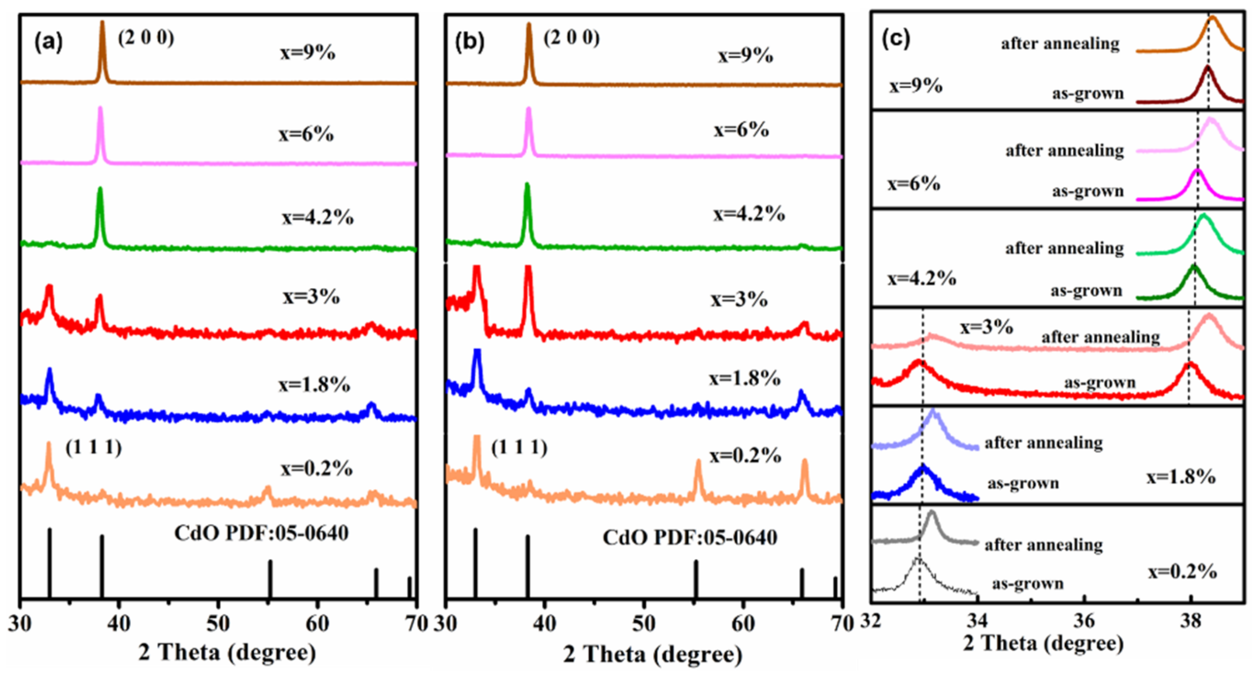
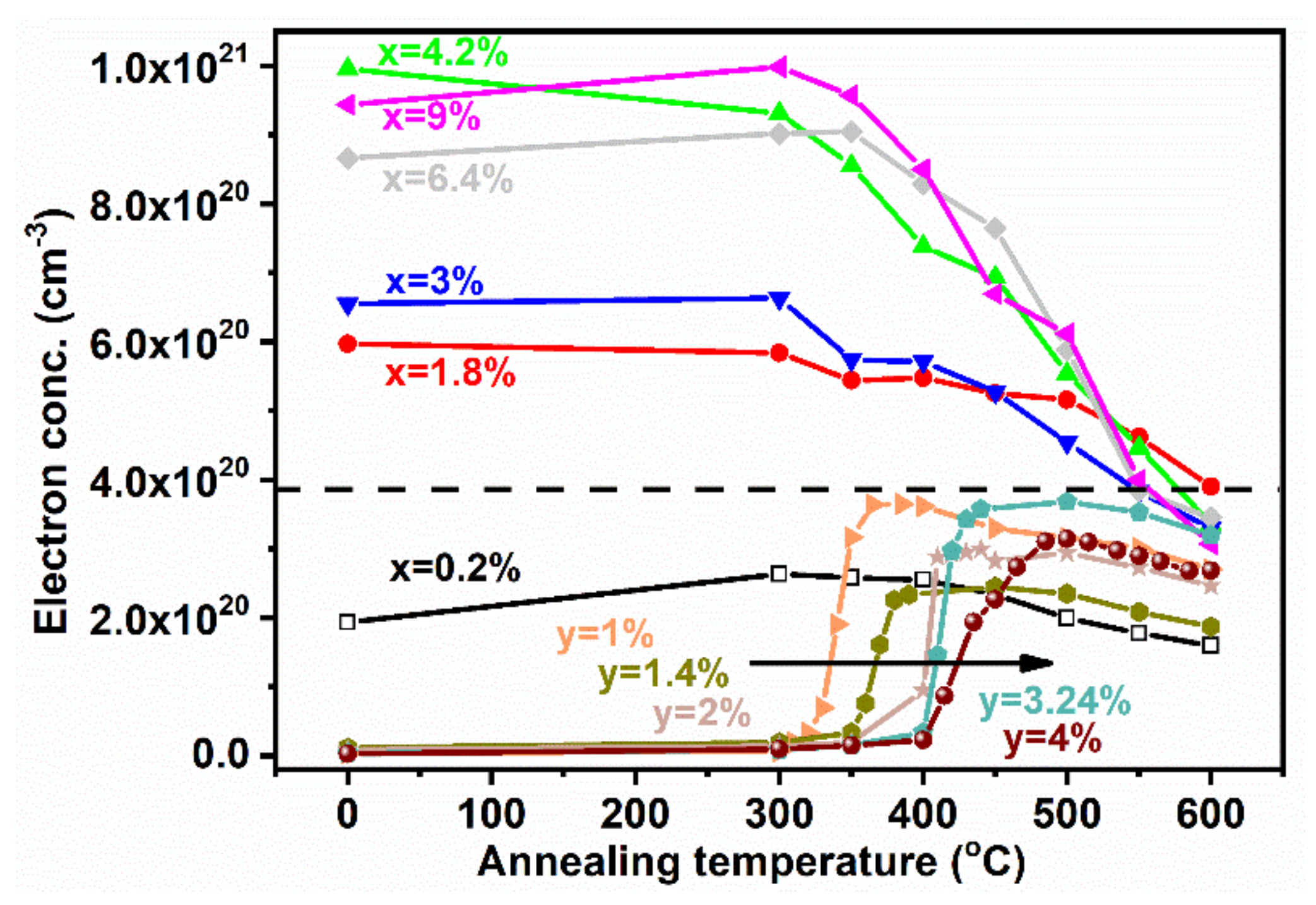
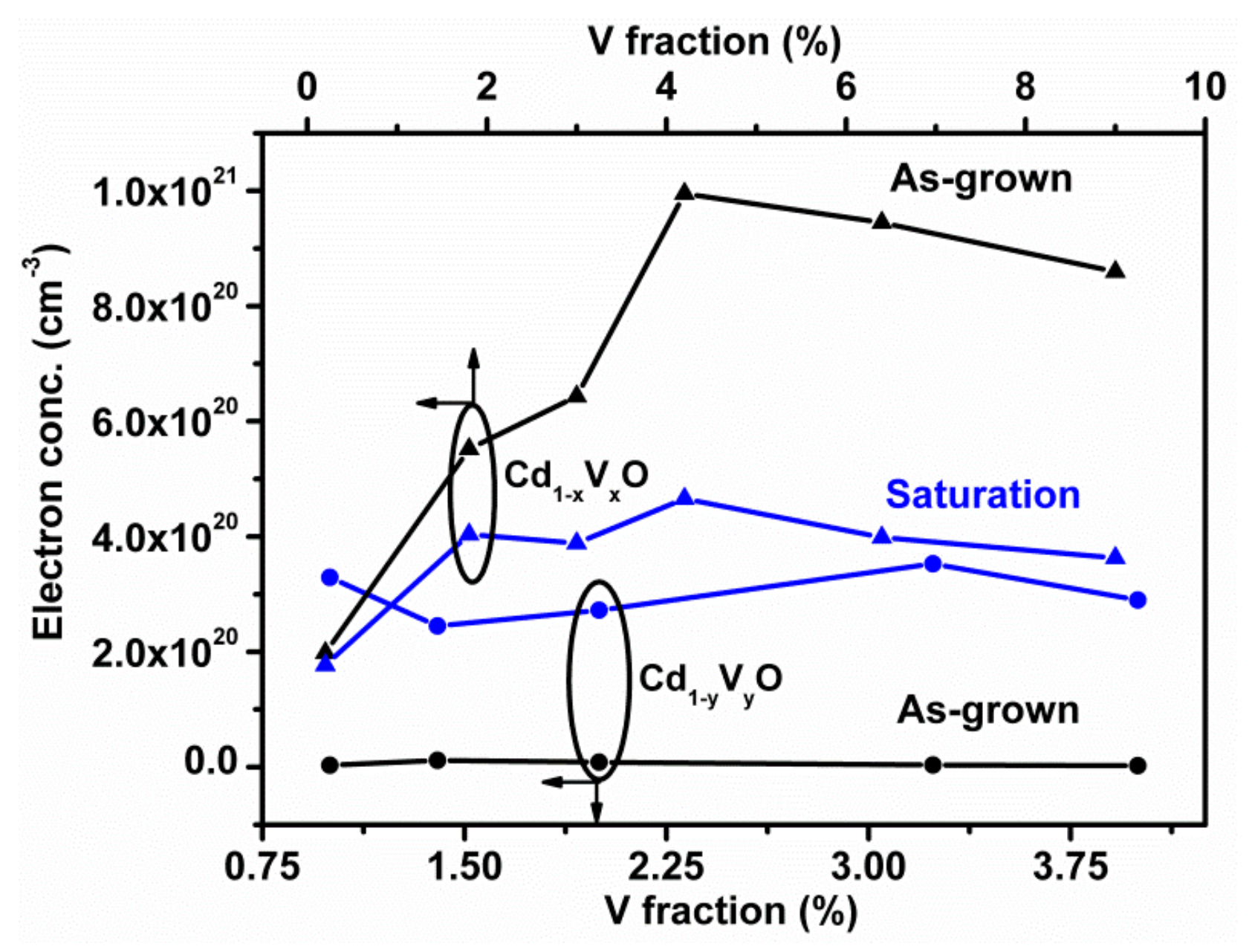
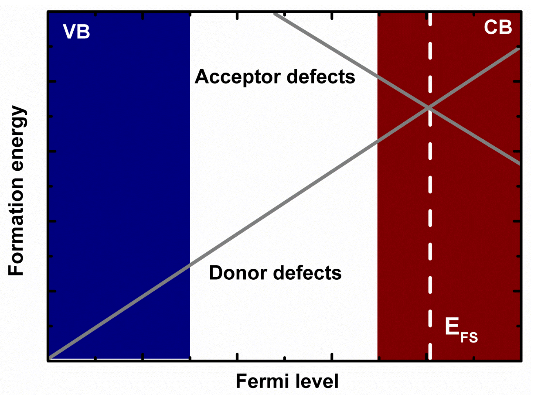
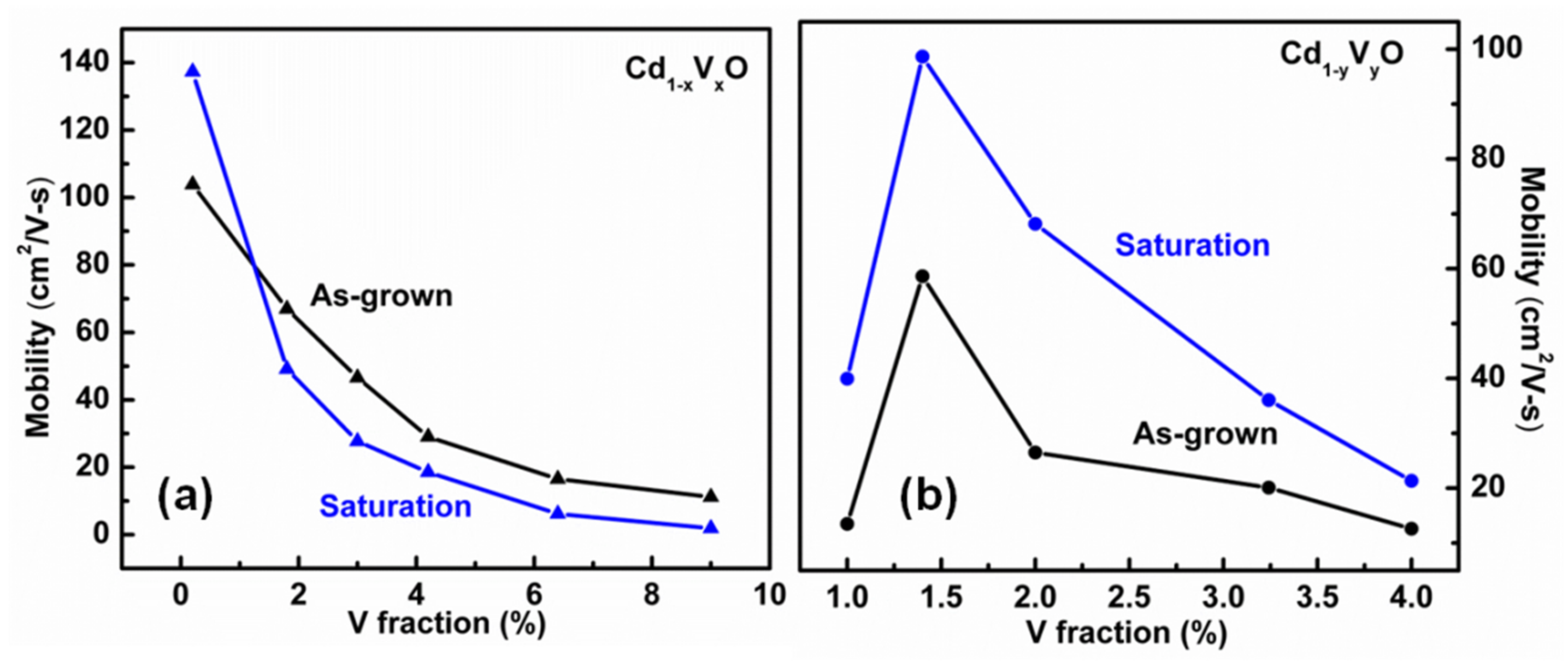
3. Results and Discussion

From RBS results, we arrive at the film thickness in the range of 150~200 nm. Meanwhile, the Ar-deposited composition with x = 0.2~9% and the Ar/O2 deposited composition with y = 1~4% are also determined.
Figure 1a,b show the XRD patterns of as-grown and annealed Cd1−xVxO (x = 0.2~9%). With increasing V fraction up to 9%, all of the as-grown and annealed films are pure phase and match well with the rocksalt CdO. The preferred orientation in film growth changes gradually from (111) to (200) with increasing V, and the turning point in both of the two series is x = 3%. V enter into the CdO lattice and are supposed to substitute for Cd sites based on electronegativity. Comparing the annealed sample with the as-grown one, both of the diffraction peaks (111) and (200) shift to a higher 2θ angle, as shown in Figure 1c. This can be understood by the Bragg equation: 2dsinθ = nλ, where d is the spacing between the planes in the atomic lattice, θ is the angle between the incident ray and the scattering planes, n is an integer, and λ denotes the wavelength of incident wave. Since the ionic radius of V (0.79 Å, 6-coord.) is smaller than Cd (0.95 Å, 6-coord.), d should decrease with more V substituting for Cd sites, which results in the increase of 2θ. This indicates that annealing induces mores V substituting for Cd sites. The XRD of Cd1−yVyO films shows a similar tendency.
Figure 2 shows the effect of annealing temperature on electron concentration in Cd1−xVxO and Cd1−yVyO series. As can be seen, all of the initial electron concentrations of Cd1−xVxO are much higher than that of Cd1−yVyO. V was supposed to behave as donor for CdO in our previous report, which could donate electrons to the charge carrier. However, a part of V donors is probably passivated by the additional O2 atmosphere [14,15], thereby lower electron concentration is obtained in Ar/O2-deposited samples. The initial electron concentration of 0.2%V-doped CdO (Ar) is as low as the undoped CdO due to the very low doping level, which makes this sample exhibit similar properties as pure CdO with annealing. With increasing annealing temperature, the electron concentrations of Cd1−xVxO samples with initial values higher than 4 × 1020 cm−3 show gradual reduction until ~4 × 1020 cm−3 at 500 °C. Meanwhile, it is noted that Cd1−yVyO samples exhibit dramatic increase in electron concentrations until ~4 × 1020 cm−3 in the temperature range 350~450 °C and then plateau, further increasing temperature results in slightly reduced electron concentrations. Furthermore, it is obvious that the “jump temperature” which is used to describe the rapid increase in electron concentration happening to Cd1−yVyO samples gradually increases from 350 °C to 375 °C, 410 °C, 420 °C and 450 °C when increasing the V fraction from 1% to 1.4%, 2%, 3.24% and 4%, respectively. This tendency is represented by the arrow in Figure 2. In summary, after annealing, the high (low) electron concentrations in Ar (Ar/O2)-deposited V-doped CdO downward (upward) shift to a saturation value at an annealing temperature of 500 °C. In addition, the very low V-doped sample (x = 0.2%) keeps a stable electron concentration at around 2 × 1020 cm−3 with annealing.
In order to obtain more detailed information about the saturated electron concentration in these two series, long-time annealing at 500 °C is performed. The saturated electron concentrations, obtained at as long at time as 600 s annealing as a function of V fraction, are shown in Figure 3. Except for the very low V doped sample (x = 0.2%), other Ar-deposited samples with electron concentrations higher than 4 × 1020 cm−3 and Ar/O2-deposited samples with electron concentrations lower than 4 × 1020 cm−3 follow the decreasing and increasing tendencies, respectively. Finally, they saturate at ~4 × 1020 cm−3, which can be understood through the amphoteric defect model.
Figure 4 gives the simplified amphoteric defect model of CdO [16,17]. The formation energy for donor (acceptor) native defects increases (decreases) with the increasing Fermi level, such that formation of donor (acceptor) native defects is most favorable when the Fermi level is below (above) an energy level known as the Fermi-level stabilization energy (EFS) [16,17], denoted as the white dashed line in Figure 4. This level makes the energy at which their character changes, from predominantly donor-like (valence band character) below EFS to predominantly acceptor-like (conduction band character) above the EFS [17]. Consequently, we can obtain the equal formation energies for donor and acceptor native defects at EFS, which means the number of formed donors can balance with that of formed acceptors and no change happens in carrier density when further creating native defects at this point [17]. The EFS is located substantially above the conduction band minimum (CBM) in CdO due to its extremely low CBM, which is different to most conventional semiconductors whose EFS is normally located close to the middle of the fundamental band gap [18] This particular location of EFS in CdO results in the formation energy for compensating acceptor (donor) defects being relatively high (low) with n-type (p-type) doping, allowing CdO to be extrinsically heavily n-type doped, thus p-type CdO is always difficult to achieve [19]. The exact location of EFS in CdO has been determined through the ionic irradiation induced defects which results in the electron concentration stabilizing at a saturation level of ~5 × 1020 cm−3 [20]. Our annealed results are close to EFS of CdO. RTA can fulfill high temperature annealing in a very short time, which results in the reduced defects and improved crystallization properties with minimal dopant redistribution [21]. The thermal energy provided by RTA is able to induce the thermodynamic system to reach equilibrium. Combined with the amphoteric defect model, the electron concentrations of Ar-deposited Cd1−xVxO (x > 0.2%) series with value higher than 4 × 1020 cm−3 have the tendency to go down and saturate at EFS level with the assistance of native acceptors (V vacancy, Cd vacancy or O interstitial) after annealing. As a result, the electron concentrations of these samples stabilize near EFS after long-time annealing at 500 °C. However, the electron concentrations of Cd1−yVyO series with low original electron concentrations in the range of 1018~1019 cm−3 show rapid increase at certain points and then saturate close to the EFS level with time-dependent annealing. During the annealing process, some passivated V species are probably activated under N2 background, then behave as donors to denote electrons to the charge carrier, resulting in increased electron concentrations.
It is worth noting that the “jump temperature” increases from 350 °C to 450 °C with increasing V concentration in Cd1−yVyO series. This means the barrier energy enhances gradually with V doping, which can be calculated through the Arrhenius equation [22].
1 = w O P F × exp ( Δ E k B T )
where wOPF is the optical phonon frequency of CdO with a value of 9.06 × 10¹³ s−1, kB is Boltzmann constant, T is the temperature to overcome the energy barrier and ΔE is the barrier energy. As a result, the calculated ΔE increases linearly from 1.72 eV to 1.79 eV, 1.89 eV, 1.91 eV and 2.00 eV with the V fraction increasing from 1% to 1.4%, 2%, 3.24% and 4%, respectively, indicating that more energy is required to overcome the barrier in order to reach equilibrium when increasing doped V. The reason for the very low V-doped sample (x = 0.2%), almost keeping stable electron concentration at around 2 × 1020 cm−3 with annealing, is because the doped V level is too low to influence the basic electrical properties of CdO.
Based on the above discussion, it is reasonable to check the mobility tendencies to confirm our deduction. Figure 5a,b show the saturated mobility of Cd1−xVxO and Cd1−yVyO after long time annealing at 500 °C, respectively. As-grown mobility is also shown as references. For Cd1−xVxO, the mobility exhibits fast reduction after annealing and becomes smaller than the as-grown ones when x > 0.2%, even though RTA could increase the mobility through reduced defects and improved crystallization properties, which is confirmed by the enhanced mobility in the x = 0.2% sample after annealing. However, for Ar/O2-deposited series, mobility increases greatly after annealing. From the amphoteric defect model, it has been suggested that the nature of formed native defects in Ar-deposited series is acceptor and in Ar/O2-deposited series is donor. Both electron concentration and scattering centers are strongly dependent on the formed defects, which can be expressed as [23].
n = da
Ni = d + a
where d and a denote the number of donors and acceptors, respectively, n is electron concentration and Ni is scattering centers. As the favorably formed defects, acceptors in Ar-deposited series increase greatly after annealing, meanwhile reducing the electron concentration, which is in accord with the result in Figure 2. On the other hand, the increased acceptors would produce more scattering centers and then reduce mobility. Such an effect surpasses the improved mobility from better crystalline, and overall exhibits rapid reduction in mobility. This tendency further confirms the conclusion from the amphoteric defect model. For Ar/O2-deposited samples, donors are the usually formed defects after annealing. From Equation (3), the increased donors are expected to increase scattering centers and then reduce mobility if no change happens to the acceptors. However, the mobility increases greatly after annealing; this indicates that more acceptors may disappear in this process, which could compensate party for the donors. As a result, the overall scattering centers decrease and mobility increases. On the other hand, the combined effects of increased donors and reduced acceptors could finally result in the enhanced electron concentration from Equation (2). This is also verified in Figure 2.

4. Conclusions

Ar-deposited Cd1−xVxO and Ar/O2 deposited Cd1−yVyO show higher and lower electron concentrations than 4 × 1020 cm−3, respectively. V behave as donors for CdO which are probably passivated by O2 in the synthesis process, resulting in much lower electron concentrations in Ar/O2-deposited series than in Ar-deposited series. After annealing in N2, the electron concentrations of the two series reduce or increase to a saturated value of ~4 × 1020 cm−3, which is close to EFS. Based on the amphoteric defect model, the favorably formed defects for Ar-deposited and Ar/O2-deposited series during annealing are acceptors and donors, respectively. This is also confirmed through the combined results of the changing tendency in electron concentration and mobility.

Author Contributions

Conceptualization: Y.L.; Data curation: G.C.; Formal analysis: K.Y.; Resources: W.W.; Software: W.G. All authors have read and agreed to the published version of the manuscript.

Funding

This research was funding by National Natural Science Foundation of China (No. 51602121) and PhD Start-up Program of Huizhou University (No. 2016JB006).

Institutional Review Board Statement

Not applicable.

Informed Consent Statement

Not applicable.

Data Availability Statement

The data presented in this study is available within the article.

Acknowledgments

This work was supported by the U.S. Department of Energy, Office of Science, Basic Energy Sciences, Materials Sciences Engineering Division, China Scholarship Council, National Natural Science Foundation of China (No. 51602121), Guangdong Provincial Natural Science Foundation Project (No.2021A1515010282) and PhD Start-up Program of Huizhou University (No. 2016JB006). This work was also supported by Program for Innovative Research Team of Guangdong Province & Huizhou University (IRTHZU).

Conflicts of Interest

The authors declare no conflict of interest.

References

  1. Ismail, R.A. Improved characte ristics of sprayed CdO films by rapid thermal annealing. J. Mater. Sci. Mater. Electron. 2019, 20, 1219–1224. [Google Scholar] [CrossRef]
  2. Franco-Linton, B.; Castanedo-Pérez, R.; Torres-Delgado, G.; Márquez-Marín, J.; Zelaya-Ángel, O. Influence of vacuum and Ar/CdS atmospheres-rapid thermal annealing (RTA) on the properties of Cd2SnO4 thin films obtained by sol-gel technique. Mater. Sci. Semicond. Process. 2016, 56, 302. [Google Scholar] [CrossRef]
  3. Xie, M.T.; Zhu, W.; Yu, K.M.; Zhu, Z.S.; Wang, G.Z. Fe-embedded Au (111) monolayer as an electrocatalyst for N2 reduction reaction: A first-principles investigation. J. Alloys Compd. 2019, 776, 259. [Google Scholar] [CrossRef]
  4. Morales, G.E.M.; Garcia, M.E.A.; Cruz, S.C.; Plata, B.R.; Moreno, O.P.; Pérez, R.G. CdCO3 nanocrystalline thin film grown by chemical bath and its transition to porous CdO by thermal annealing treatment. Optik 2018, 171, 347–355. [Google Scholar] [CrossRef]
  5. Yu, K.M.; Detert, D.M.; Chen, G.B.; Zhu, W.; Liu, C.P.; Grankowska, S.; Hsu, L.; Dubon, O.D.; Walukiewicz, W. Defects and properties of cadmium oxide based transparent conductors. J. Appl. Phys. 2016, 119, 18150. [Google Scholar] [CrossRef]
  6. Yu, K.M.; Mayer, M.A.; Speaks, D.T.; He, H.; Zhao, R.; Hsu, L.; Mao, S.S.; Haller, E.E.; Walukiewicz, W. Ideal transparent conductors for full spectrum photovoltaics. J. Appl. Phys. 2012, 111, 123505. [Google Scholar] [CrossRef]
  7. Segura, A.; Sanchez-Royo, J.F.; Garia-Domene, B.; Almonacid, G. Current underestimation of the optical gap and Bursterin-Moss shift in CdO thin films: A consequence of extended misuse of α2-versus-hν plots. Appl. Phys. Lett. 2011, 99, 151907. [Google Scholar] [CrossRef]
  8. Li, Y.J.; Yu, K.M.; Chen, G.B.; Liu, C.P.; Walukiewicz, W. Conduction band modifications by d states in vanadium doped CdO. J. Alloys Compd. 2020, 822, 153567. [Google Scholar] [CrossRef]
  9. Yu, J.H.; Kim, J.H.; Park, D.S.; Jeong, T.S.; Youn, C.J.; Hong, K.J. Effect of rapid thermal annealing on Zn1−xCdxO layers grown by radio-frequency magnetron co-sputtering. Cryst. Res. Technol. 2010, 45, 1050–1056. [Google Scholar] [CrossRef]
  10. Sakthivel, P.; Murugan, R.; Asaithambi, S.; Karuppaiah, M.; Rajendran, S.; Ravi, G. Radio frequency magnetron sputtered CdO thin films for optoelectronic applications. J. Phys. Chem. Solids 2019, 126, 1–10. [Google Scholar] [CrossRef]
  11. Saha, B.; Thapa, R.; Chattopadhyay, K.K. Wide range tuning of electrical conductivity of RF sputtered CdO thin films through oxygen partial pressure variation. Sol. Energy Mater. Sol. Cells 2008, 92, 1077–1080. [Google Scholar] [CrossRef]
  12. Sakthivela, P.; Murugana, R.; Asaithambia, S.; Karuppaiaha, M.; Rajendrana, S.; Ravi, G. Influence of radiofrequency power on structural, morphological, optical and electrical properties of magnetron sputtered CdO: Sm thin films as alternative TCO for optoelectronic applications. J. Alloys Compd. 2018, 765, 146. [Google Scholar] [CrossRef]
  13. Devika, M.; Koteeswara, N.; Reddy, S.; Venkatramana Reddy, K.; Ramesh, K.; Gunasekhar, R. Influence of rapid thermal annealing (RTA) on the structural and electrical properties of SnS films. J. Mater. Sci. Mater. Electron. 2009, 20, 1129. [Google Scholar] [CrossRef]
  14. Huang, T.Z.; Yuan, X.X.; Yu, J.M.; Wu, Z.; Han, J.T.; Sun, G.X.; Xu, N.X.; Zhang, Y.H. Effects of annealing treatment and partial substitution of Cu for Co on phase composition and hydrogen storage performance of La0.7Mg0.3Ni3.2Co0.35 alloy. Int. J. Hydrogen Energy 2012, 37, 1074. [Google Scholar] [CrossRef]
  15. Silversmit, G.; Depla, D.; Poelman, H.; Marin, G.B.; Gryse, R.D. Determination of the V2p XPS binding energies for different vanadium oxidation states (V5+ to V0+). J. Electron Spectrosc. Relat. Phenom. 2004, 135, 167–175. [Google Scholar] [CrossRef]
  16. Kwon, H.; Thompson, L.T.; Eng, J., Jr.; Chenz, J.G. n-Butane dehydrogenation over vanadium carbides: Correlating catalytic and electronic properties. J. Catal. 2000, 190, 60–68. [Google Scholar] [CrossRef]
  17. Walukiewicz, W. Amphoteric native defects in semiconductors. Appl. Phys. Lett. 1989, 54, 2094–2096. [Google Scholar] [CrossRef] [Green Version]
  18. King, P.D.C.; Veal, T.D.; Jefferson, P.H.; Zúñiga-Pérez, J.; Muñoz-Sanjosé, V.; McConville, C.F. Unification of the electrical behavior of defects, impurities, and surface states in semiconductors: Virtual gap states in CdO. Phys. Rev. B 2009, 79, 035203. [Google Scholar] [CrossRef] [Green Version]
  19. Langer, J.M.; Delerue, C.; Lannoo, M. Transition-metal impurities in semiconductors and heterojunction band lineups. Phys. Rev. B 1998, 38, 7723. [Google Scholar] [CrossRef] [PubMed]
  20. Burbano, M.; Scanlon, D.O.; Watson, G.W. Sources of conductivity and doping limits in CdO from hybrid density functional theory. J. Am. Chem. Soc. 2011, 133, 15065–15072. [Google Scholar] [CrossRef]
  21. Speaks, D.T.; Mayer, M.A.; Yu, K.M.; Mao, S.S.; Haller, E.E.; Walukiewicz, W. Fermi level stabilization energy in cadmium oxide. J. Appl. Phys. 2010, 107, 113706. [Google Scholar] [CrossRef] [Green Version]
  22. Seidel, T.E.; Lischner, D.J.; Pai, C.S.; Lau, S.S. Temperature transients in heavily doped and undoped silicon using rapid thermal annealing. J. Appl. Phys. 1985, 57, 1317–1321. [Google Scholar] [CrossRef]
  23. Laidler, K.J. The development of the Arrhenius equation. J. Chem. Educ. 1984, 61, 494. [Google Scholar] [CrossRef]
Figure 1. XRD of Cd1−xVxO (x = 0.2~9%): as-grown films (a); annealed films (b); comparison of as-grown and annealed films in 2θ range of 32~39° (c).
Crystals 11 01079 g001
Figure 2. Electron concentrations of Cd1−xVxO (x = 0.2~9%) and Cd1−yVyO (y = 1~4%) series as a function of annealing temperature when annealed for 20 s.
Crystals 11 01079 g002
Figure 3. Saturated electron concentrations in Cd1−xVxO (x = 0.2~9%) and Cd1−yVyO (y = 1~4%) series; as-grown are also shown.
Crystals 11 01079 g003
Figure 4. Schematic representation of the formation energy as a function of Fermi level in CdO. The CB and VB are represented by red and blue shading, respectively.
Crystals 11 01079 g004
Figure 5. As-grown and saturated mobility in Cd1−xVxO (x = 0.2~9%) (a) and Cd1−yVyO (y = 1~4%) series (b).
Crystals 11 01079 g005
Publisher’s Note: MDPI stays neutral with regard to jurisdictional claims in published maps and institutional affiliations.

