Abstract
We report fabrication of large-scale homogeneous crystallization of CH3NH3PbBr3 (MAPbBr3) in the patterned substrate by a two-dimensional (2D) grating. This achieves high-quality optotelectronic structures on local sites in the micron scales and a homogeneous thin-film device in a centimeter scale, proposing a convenient technique to overcome the challenge for producing large-area thin-film devices with high quality by spin-coating. Through matching the concentration of the MAPbBr3/DMF solutions with the periods of the patterning structures, we found an optimized size of the patterning channels for a specified solution concentration (e.g., channel width of 5 μm for a concentration of 0.14 mg/mL). Such a design is also an excellent scheme for random lasing, since the crystalline periodic networks of MAPbBr3 grids are multi-crystalline constructions, and supply strong light-scattering interfaces. Using the random lasing performance, we can also justify the crystallization qualities and reveal the responsible mechanisms. This is important for the design of large-scale optoelectronic devices based on thin-film hybrid halide perovskites.
1. Introduction
Organic-inorganic hybrid halide perovskites are a group of promising semiconductor materials for high-efficiency optoelectronic devices [1,2,3,4,5,6]. Light-emitting [7,8,9] and photovoltaic [10,11,12] diodes, as well as lasing devices [13,14,15,16,17], have been reported on extensively. Although single- or multi-crystals have been synthesized in large scales at high quality [18,19,20,21,22] and have been applied for various purposes, thin-film devices [23,24,25,26] are more attractive in the construction of devices that are integratable into micro- or nano-scale systems. However, the conventional spin-coating method may encounter problems with the homogeneity of the produced film, in particular for large-scale fabrication. This is not only because of the dewetting of the solution on the conventional substrates, but also due to the quick crystallization of the molecules in random scales and random distributions.
Patterning the substrate with designed micro- or nano-structures and optimized microscopic dimensions may not only modify its surface-energy properties, but also control the molecular crystallization process by dividing the large-area surface into periodic/nonperiodic localized sites. This is an ideal strategy to achieve large-area thin films with high qualities precisely controllable on each local site. Such a strategy applies not only to hybrid halide perovskites [27] but also to any other organic/inorganic semiconductors [28,29] or even biomolecules [30] with strong aggregation performance. The corresponding designs also simultaneously facilitate new functions, including micro-/nano-cavity effects, local-field confinement, output coupling control, optical waveguides, and interface structural optimization or metasurface incorporation [31]. We have recently reported controllable crystallization of the hybrid halide perovskites into grating lines with continuous distribution over a large length scale [27], which provides an effective approach to overcome the above-mentioned challenge for producing high-quality MAPbBr3 crystal stripe gratings with controllable performance.
In this work, we report fabrication of large-area thin films into two dimensions, which enabled strong confinement of the molecules into more localized sites, and thus higher-quality crystallization. An optimized matching was found between the solution concentration and the patterning periods, with a duty cycle of about 50%. The random lasing performance was investigated to characterize the fabricated 2D structures and to verify the responsible mechanisms. Thus, we achieved thin-film CH3NH3PbBr3 (MAPbBr3) with a homogeneous area in the scale of cm2 and locally high-quality crystalline structures in sizes of microns.
2. The Network of Squarely Gridded Thin Film of MAPbBr3
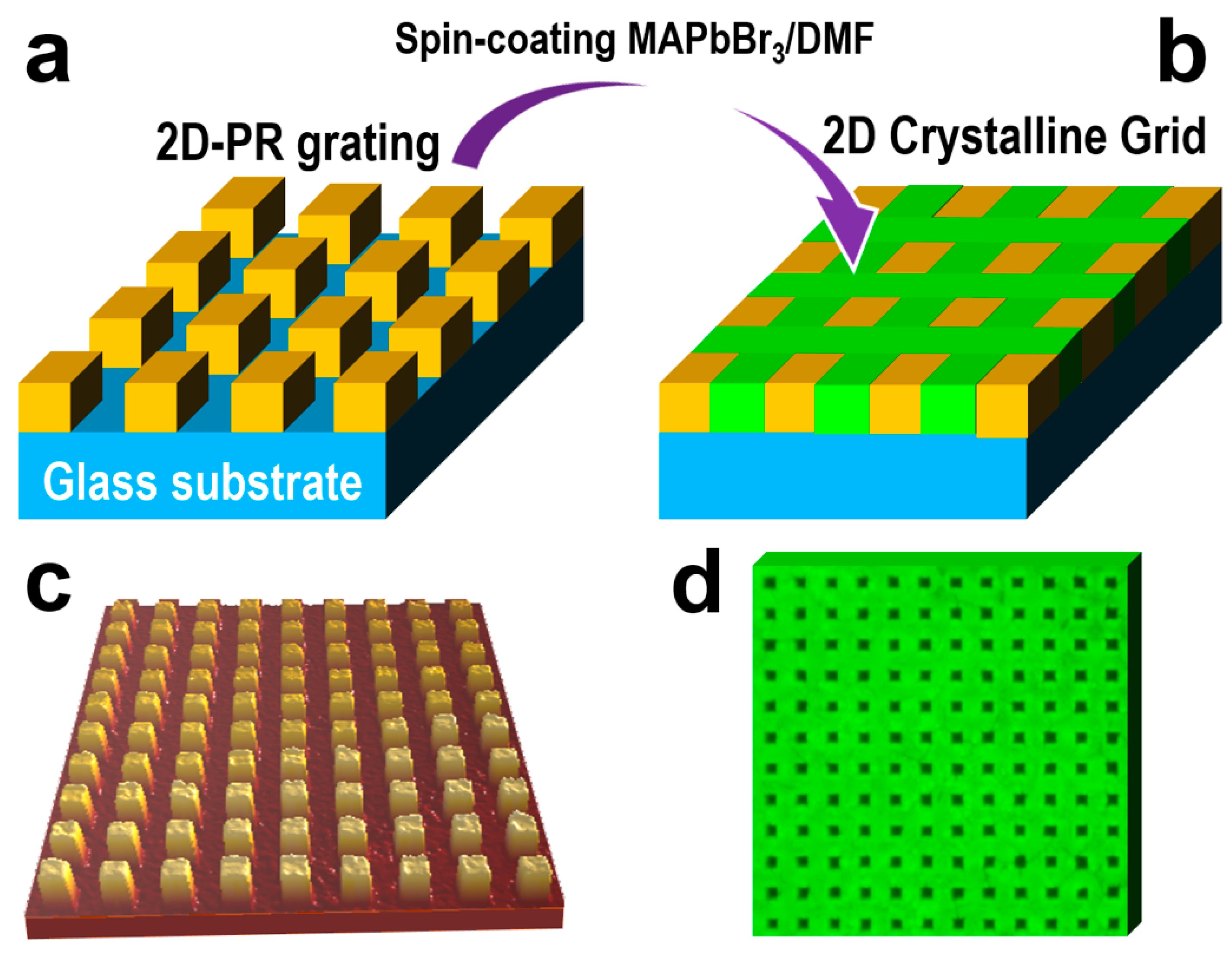
The preparation method is illustrated in Figure 1 for the gridding network of the MAPbBr3 thin film. First, a two-dimensional (2D) grating was produced by photolithography, where a positive photoresist S1805 was employed, so that the grating consists of periodically distributed square cylinders on a glass substrate, as shown in Figure 1a. Using different masks, we have fabricated gratings with different periods of 10, 20, and 50 μm. Then, the solution of MAPbBr3 in DMF with different concentrations was spin-coated onto the top surface of the grating. In the last stage, the sample was heated to 90 °C for about 60 s. Figure 1c,d shows the microscopic characterization of the template photoresist grating by 3D profiler and the finalized MAPbBr3 grating by a fluorescence optical microscope, respectively. They illustrate clearly high-quality 2D gratings of square cylinders with steep edges and homogeneous 2D grids of crystallized MAPbBr3. Since Figure 1 is used to interpret the preparation procedures, we did not present detailed parameters of the structures in Figure 1c,d. We have also found that for a concentration of 0.14 mg/mL, the gridding network surrounding the cylinders can be filled completely and homogeneously, as illustrated in Figure 1b. Higher concentrations led to inhomogeneity and connection between neighboring locations, while concentrations that were too low led to incomplete fill of the grating grooves.

Figure 1.
(a,b): Schematic illustration of the fabrication of gridded MAPbBr3 crystalline film by filling the void space in the 2D PR grating through spin-coating the MAPbBr3/DMF solution. (c) 3D topological image of the template PR grating prepared by photolithography. (d) Optical microscopic image of the fabricated 2D crystalline grid of MAPbBr3 under illumination by UV light.
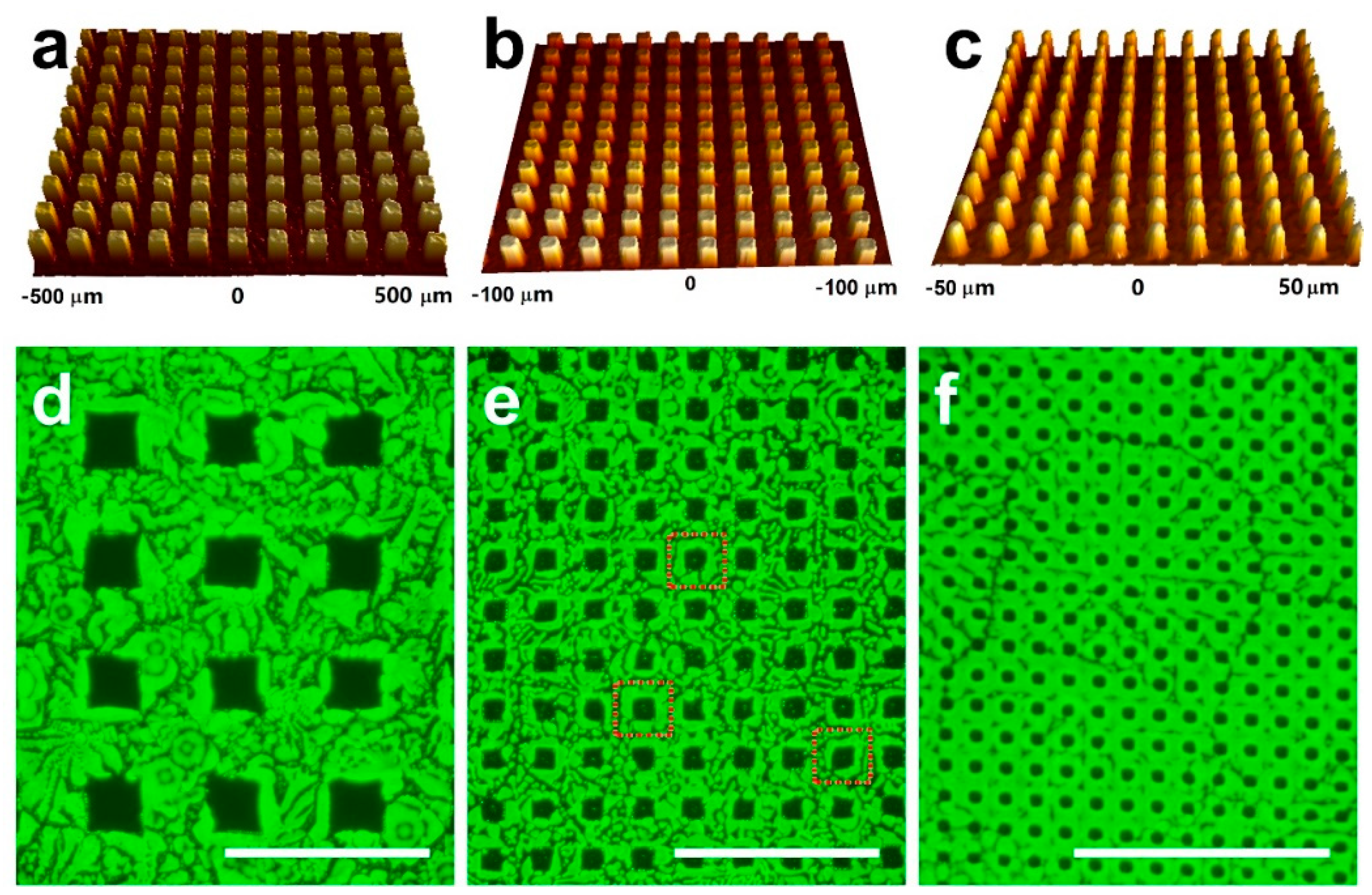
Figure 2 shows the microscopic measurements on the practically fabricated structures. Figure 2a–c show the 3D topological mapping of the photoresist grating structures for a period of 50, 20, and 10 μm by a 3D profiler, which verify excellent distribution and homogeneity performance of these grating structures. Although it is not specified in the figures for the clarity of the demonstration, according to the 3D topological measurements, the modulation depth of the gratings or the square cylinder height is about 1 μm for all of the samples. We have also carried out fabrication experiments for a larger grating period of 100 μm and smaller periods than 2 μm to optimize the structural parameters. However, we did not find much difference between the fabrication using 50 and 100 μm. In contrast, for grating periods smaller than 2 μm we did not achieve satisfying crystalline structures of MAPbBr3 on the patterned substrates. Therefore, we include in this work our fabrication and investigation of the patterned MAPbBr3 thin film by three typical periods of 10, 20, and 50 μm.

Figure 2.
3D topological images (a–c) and optical microscope images (d–f) of the template PR grating and the finished crystalline MAPbBr3 grid for periods of 50 μm, 20 μm, and 10 μm, respectively. The scale bars denote a same length scale of 80 μm.
Figure 2d–f show the fluorescence microscope images of the fabricated MAPbBr3 thin film on patterned substrates with photoresist gratings of different periods. For a grating period of 50 μm, due to the large width and large volume of the grating grooves, there are two opposite effects during the crystallization processes. On one hand, a large amount of MAPbBr3 was confined completely into the grating grooves, which favors good crystallization performance inside the large volumes. On the other hand, due to the low concentration of the solution, the materials confined in the grating groove during the spin-coating process are limited; the large volume inside the grating grooves allows more freedom and more time for MAPbBr3 to get crystallized; these factors reduce the quality and homogeneity of the crystals, as can be confirmed by Figure 2d. We can observe that all of the MAPbBr3 are confined to the grooves with very clear edges, however, defects are distributed randomly and extensively in the crystal networks, which can be identified by the dark textures on the bright green background.
Similar effects can still be observed in Figure 2e, where the grating period was reduced to 20 μm. More continuous crystals may be observed in Figure 2e than in Figure 2d, in particular in the space surrounding the photoresist square cylinders, as highlighted by dashed red squares. In contrast, when the grating period is reduced to 10 μm, the continuity and homogeneity of the crystal grid becomes much improved, as can be seen in Figure 2f. The whole network can be observed as a whole crystalline MAPbBr3 film with “black holes” punched by the photoresist square cylinders. The significantly reduced space in the grooves of the grating with a period of 10 μm enables complete filling by MAPbBr3 and high-quality crystallization with continuous connection over the whole grating structure. It is also understandable that breaks may be observed over the large-scale solid structure, as can be verified by the dark defects in Figure 2f. It is thus an indication that for a given solution concentration there exists an optimized channel width for the crystallization of MAPbBr3 in the 2D-distributed grating grooves. For a concentration of 0.14 mg/mL of MAPbBr3 in DMF, the grating period of 10 μm with a rough 50% duty cycle is found to be the best design for producing continuous crystalline structures.
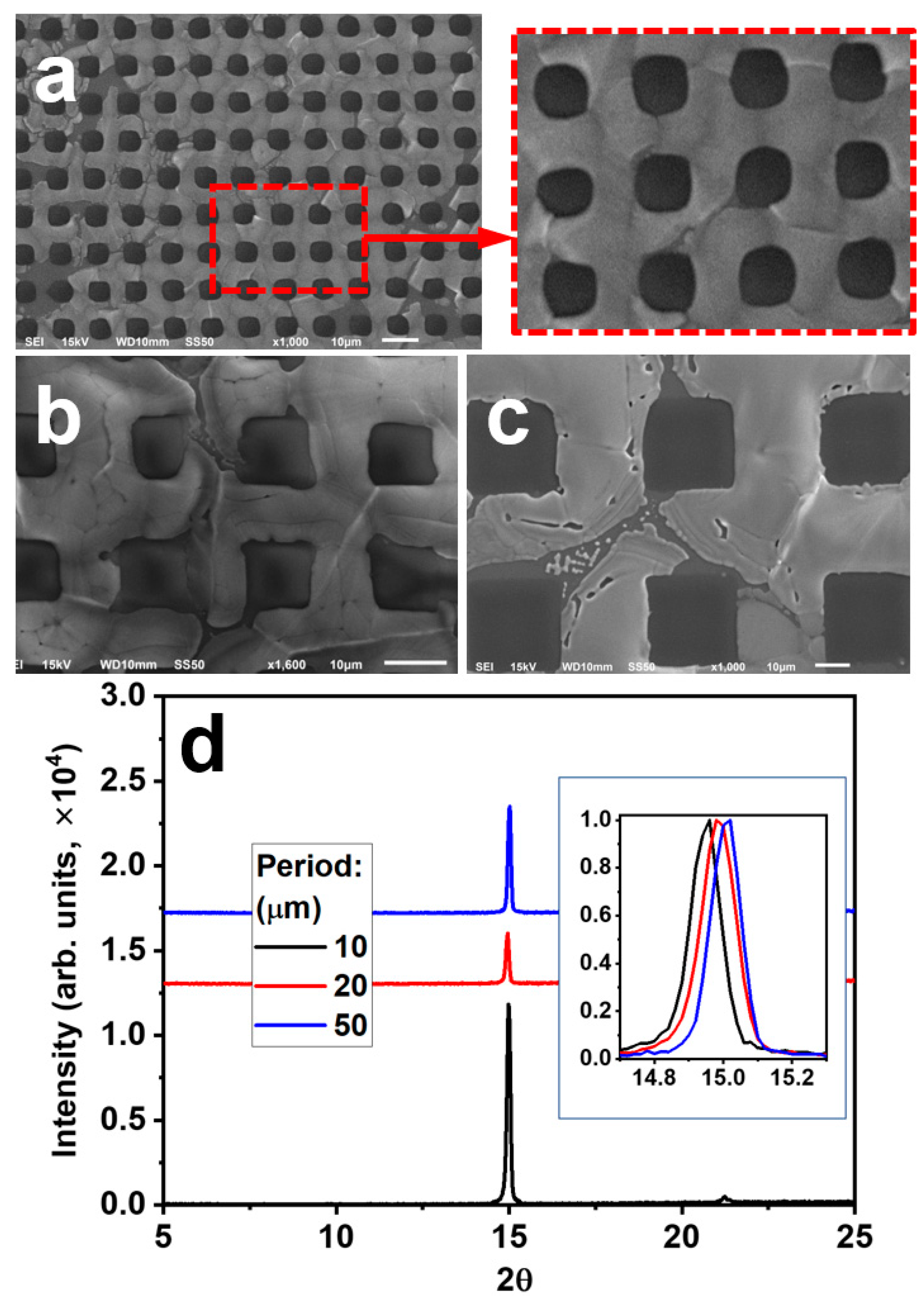
Figure 3a–c show the scanning electron microscope (SEM) images for the samples patterned with a period of 10, 20, and 50 μm, respectively. Figure 3d shows the X-ray diffraction (XRD) spectra for these three samples. According to the SEM images, the sample patterned by the 10-μm grating exhibits the best surface quality among the three samples. Looking at the XRD spectra in Figure 3d at 2θ = 15° in the inset of Figure 3d, we can find that the sample with a 10-μm has the strongest diffraction, the narrowest spectrum, and the smallest diffraction angle. This also implies the best crystalline quality among these three samples. Therefore, the experimental results in Figure 3 again confirmed our analysis above (Figure 2).

Figure 3.
(a) SEM image for the patterned structure with a period of 10 μm and an enlarged view of a local area. (b,c) SEM images for the structures with a patterning period of 20 and 50 μm, respectively. (d) XRD spectra measured on the three kinds of structures patterned at different periods. Inset: an enlarged view of the spectra.
3. Optical Spectroscopic Performance of the Gridded Crystalline Film
3.1. Absorption and Photoluminescence
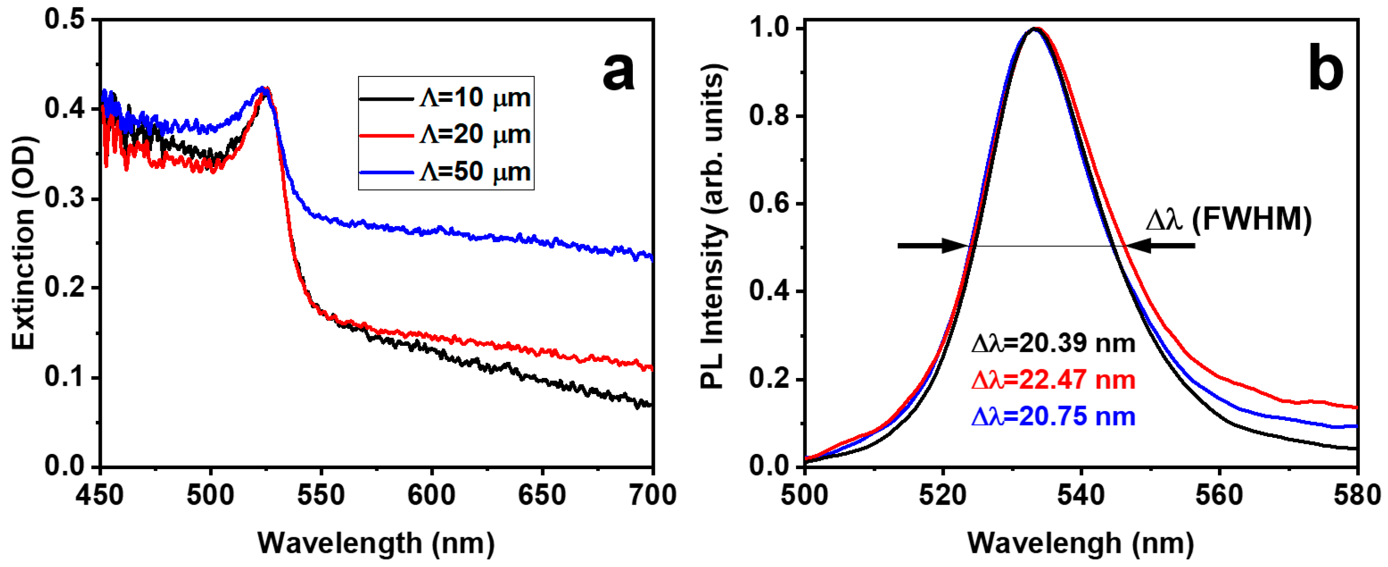
Figure 4a,b show the absorption and emission spectra of the fabricated grating structures, respectively, where the three measured spectra correspond to the samples in Figure 2d–f. According to Figure 4a, the absorption spectra of the patterned structures with different periods are peaked nearly the same at about 525 nm with a bandwidth of about 20 nm at FWHM. However, the three spectra have different contrasts, or they have different background intensity for wavelengths longer than 550 nm. Such background results mainly from the scattering of light by the patterned MAPbBr3. It is understandable by looking at the microscopic images in Figure 2, where the structures have 50 and 20 μm patterning, that they also have more inhomogeneity or defect structures than with 10 μm patterning. Meanwhile, the absorption by the 50 μm grating patterned structures has a broader absorption spectrum due to more defects or inhomogeneity than those with 20- and 10-μm patterning.
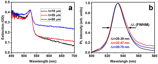
Figure 4.
Absorption (a) and PL (b) spectra of the crystalline MAPbBr3 film gridded at different periods. In (b), the bandwidth of each PL spectrum at FWHM is listed.
The PL spectra in Figure 4b are all peaked at about 533 nm, which have nearly the same spectral shape. Nevertheless, they still have slight differences in the bandwidth at FWHM, which is 20.39, 22.47, and 20.75 nm for the grating periods of 10, 20, and 50 μm. Although we did not observe a monotonic variation of the bandwidth when increasing the grating period, we can still identify a narrow emission spectrum at a grating period of 10 μm, implying more homogeneous crystallization of MAPbBr3, which can be further confirmed by the random lasing properties.
3.2. Random Lasing
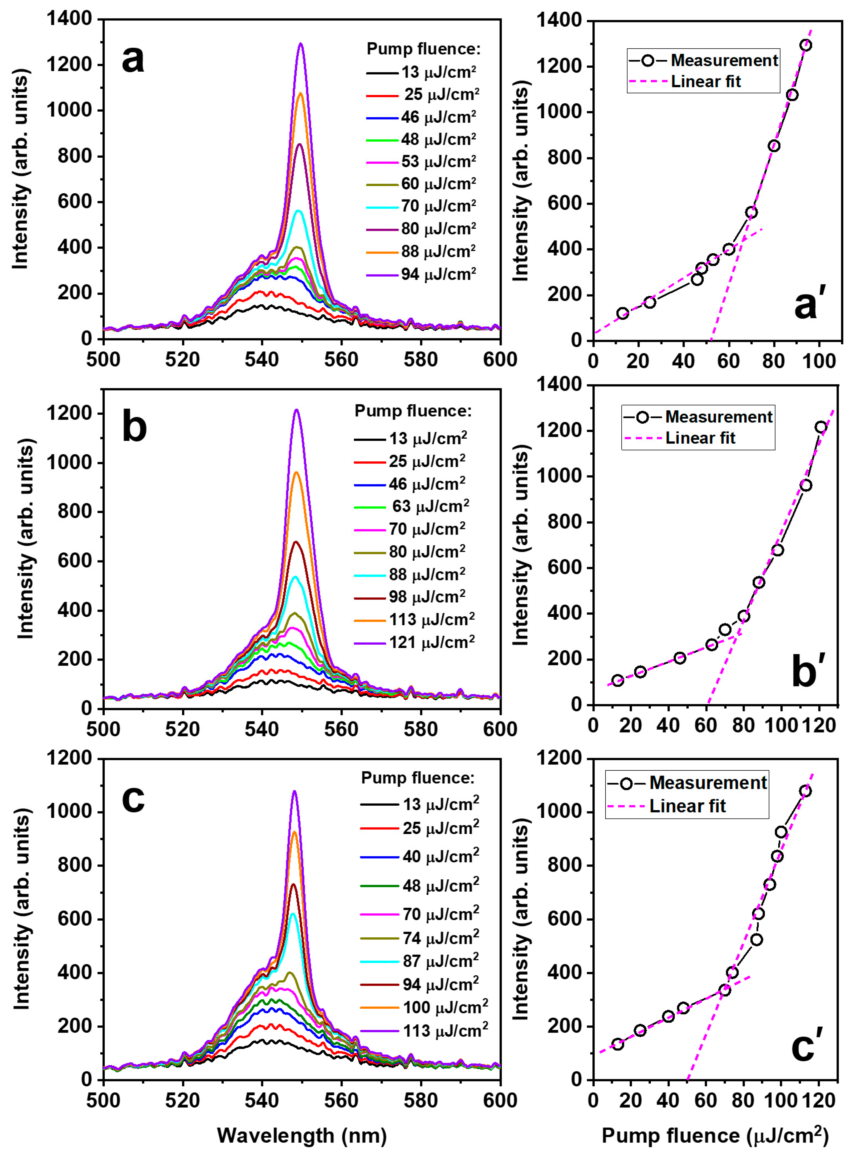
Figure 5 shows the random lasing performance of the 2D patterned structures at different periods, where Figure 5a,a’, Figure 5b,b’ and Figure 5c,c’ correspond to the grating periods of 50, 20, and 10 μm. In the measurements, a femtosecond laser with a pulse length of 150 fs, a repetition rate of 1 kHz, and a center wavelength of about 400 nm was used as the pump. A spectrometer with a sub-1 nm resolution was positioned in front of the sample and used to measure the emission spectrum. Figure 5a shows the emission spectrum measured at different pump fluence for the sample with a grating period of 50 μm. An obvious random lasing peak occurs as the pump fluence exceeds 48 μJ/cm2, which increases dramatically with the increasing of the pump fluence. The peak intensity as a function of pump fluence is plotted in Figure 5a’, where two stages can be observed, implying a clear threshold effect of the random lasing performance. Using linear fitting to the measurement data to these two stages, we can resolve a threshold pump fluence lower than 50 μJ/cm2. Similar measurements and analysis are made for the sample with a patterning period of 20 μm, as shown in Figure 5b,b’. However, a higher pump-fluence threshold can be justified for Λ = 20 μm, which is roughly 60 μJ/cm2. This can be understood by considering the lower density of defects or higher crystallization quality, as compared with Λ = 50 μm, where the light-scattering strength has been reduced and consequently the optical gain mechanisms were weakened. Similar effects apply further to the case of Λ = 10 μm, as shown in Figure 5c,c’, where random lasing spectrum can be clearly observed when the pump fluence is increased to about 70 μJ/cm2. This aligns well with the observation of the most homogeneous crystallization structures for Λ = 10 μm. All of the experimental results in Figure 5 have shown clear threshold effects and two-stage variations of the emission intensity with pump fluence, indicating excellent random-lasing performance for all of the samples. In particular, the random lasing performance supplies a further verification of the crystallization qualities at different pattering periods.
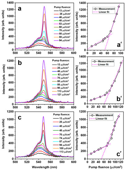
Figure 5.
Random lasing performance (emission spectra and lasing threshold) of the MAPbBr3 crystalline gridding at different periods: (a) Λ = 50 μm; (b) Λ = 20 μm; (c) Λ = 10 μm. (a’–c’) Emission intensity at about 550 nm as a function of the pump fluence, corresponding to (a–c), respectively.
A more convincing analysis is the comparison of the lasing bandwidth. To make this comparison more objective, we need to isolate the random lasing spectrum from the emission spectrum. This can be done using the mathematics below:
where IRL(λ) is the pure random lasing spectrum, I(λ) is the directly measured emission spectrum, I0(λ) is the background fluorescence spectrum at the lowest pump fluence below the threshold for random lasing, and I(535 nm) and I0(535 nm) are the intensities of the corresponding spectra at 535 nm, which is outside the spectral range of random lasing.
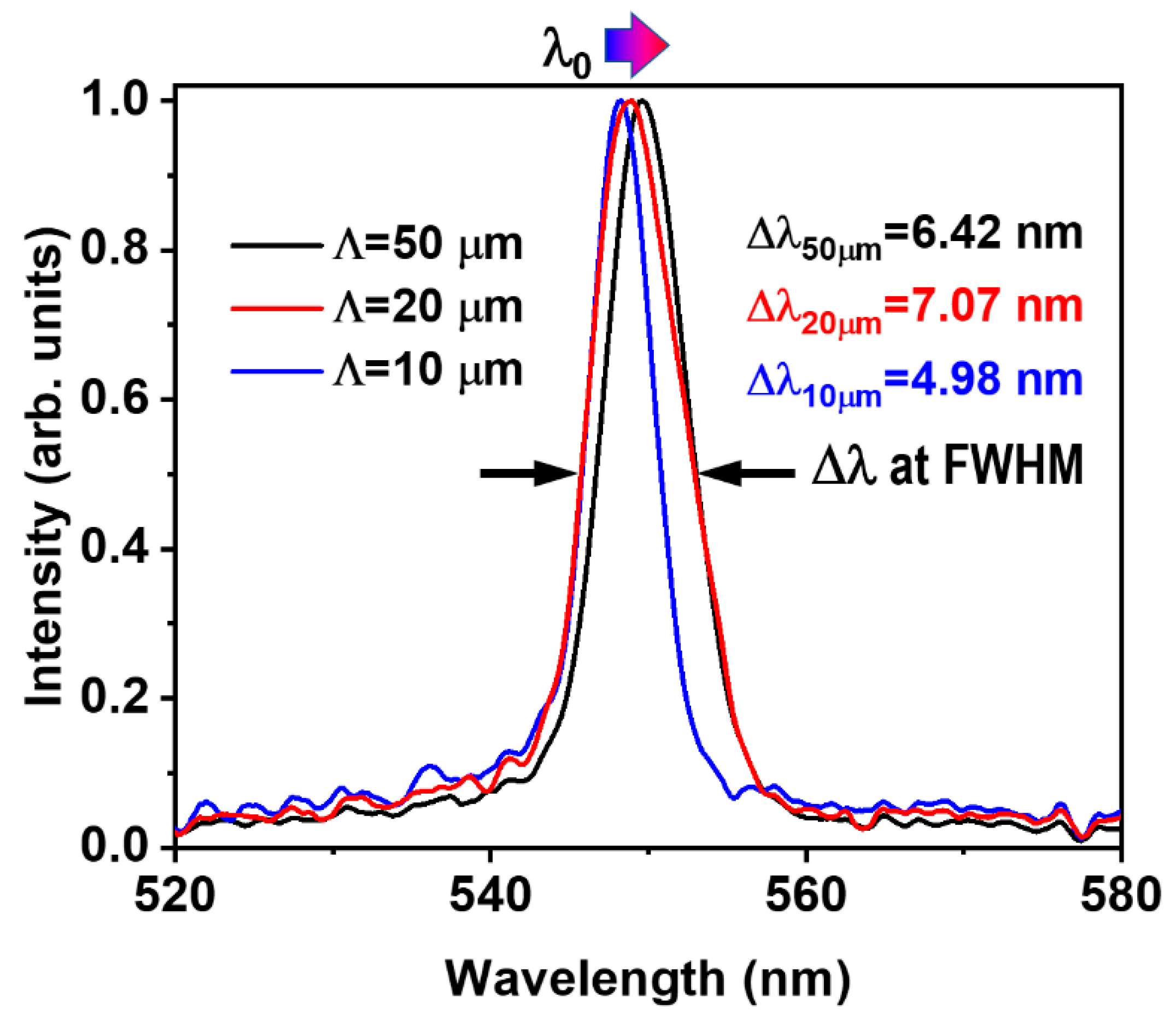
Figure 6 shows the extracted pure random lasing spectra for patterning periods of 50, 20, and 10 μm. There is observed a slight redshift of the peak wavelength (λ0) of the lasing spectrum with increasing the pattering period. However, we did not observe a monotonic variation of the lasing bandwidth, where we have a full bandwidth at half maximum of 6.42, 7.07, and 4.98 nm for the patterning periods of Λ = 50, 20, and 10 μm, respectively. Nevertheless, for Λ = 10 μm, we achieved the narrowest lasing emission spectrum. This verifies again that the structures with a period of 10 μm have the best crystallization quality and the highest homogeneity, so that the lasing spectrum has a narrowest bandwidth of 4.98 nm.
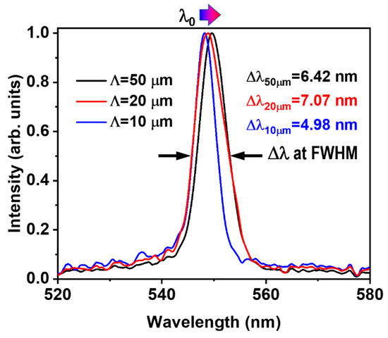
Figure 6.
Comparison between the bandwidth of the random lasing spectra measured on the patterned MAPbBr3 crystalline film at different gridding periods.
4. Conclusions
We achieved locally high-quality and large-scale homogeneous crystalline networks of MAPbBr3. This overcomes the challenge of producing large-area thin film devices of hybrid halide perovskites with high quality by spin-coating. At a specific concentration of MAPbBr3 in DMF, the optimized crystal networks were produced in a 2D grating with a period of 10 μm. Random lasing was achieved for all of the two-dimensionally gridded MAPbBr3 crystals with a period of Λ = 10, 20, and 50 μm. However, the lowest lasing threshold was measured for Λ = 50 μm and the narrowest lasing bandwidth was obtained at Λ = 10 μm. The underlying mechanism is that the strong scattering of light by high density of defects with rough interfaces enables the lowest lasing threshold at Λ = 50 μm, while the most homogeneous crystal structures allow random lasing with the narrowest bandwidth at Λ = 10 μm. These discoveries are important for the design of optoelectronic devices based on large-scale MAPbBr3 crystalline films with high quality and high homogeneity.
Author Contributions
Conceptualization, X.Z. and H.X.; methodology, X.Z. and J.H.; validation, X.Z., J.H. and H.X.; formal analysis, X.Z. and J.H.; investigation, J.H. and X.Z.; resources, X.Z.; writing—original draft preparation, X.Z.; writing—review and editing, X.Z.; visualization, X.Z.; supervision, X.Z.; project administration, X.Z.; funding acquisition, X.Z. All authors have read and agreed to the published version of the manuscript.
Funding
This research was funded by National Natural Science Foundation of China, grant number 61735002, 12074020 and by Beijing Municipal Commission of Education, grant number KZ202010005002. The APC was funded by Beijing Municipal Commission of Education.
Conflicts of Interest
The authors declare no conflict of interest.
References
- Thomas, M.B.; David, A.E.; Leeor, K.; Gary, H.; David, C.H. Hybrid organic–inorganic perovskites: Low-cost semiconductors with intriguing charge-transport properties. Nat. Rev. Mater. 2016, 1, 15007. [Google Scholar]
- Jena, A.K.; Kulkarni, A.; Miyasaka, T. Halide Perovskite Photovoltaics: Background, Status, and Future Prospects. Chem. Rev. 2019, 119, 3036–3103. [Google Scholar] [CrossRef]
- Gu, Z.; Zhou, Z.; Huang, Z.; Wang, K.; Cai, Z.; Hu, X.; Li, L.; Li, M.; Zhao, Y.S.; Song, Y. Controllable Growth of High-Quality Inorganic Perovskite Microplate Arrays for Functional Optoelectronics. Adv. Mater. 2020, 32, e1908006. [Google Scholar] [CrossRef]
- Wang, K.; Xing, G.; Song, Q.; Xiao, S. Micro- and Nanostructured Lead Halide Perovskites: From Materials to Integrations and Devices. Adv. Mater. 2020, 33, e2000306. [Google Scholar] [CrossRef]
- Ahmad, R.; Surendran, A.; Harikesh, P.C.; Haselsberger, R.; Jamaludin, N.F.; John, R.; Koh, T.M.; Bruno, A.; Leong, W.L.; Mathews, N.; et al. Perturbation-Induced Seeding and Crystallization of Hybrid Perovskites over Surface-Modified Substrates for Optoelectronic Devices. ACS Appl. Mater. Interfaces 2019, 11, 27727–27734. [Google Scholar] [CrossRef]
- Cao, L.Z.; Hu, F.R.; Zhang, C.F.; Zhu, S.N.; Xiao, M.; Wang, X.Y. Optical studies of semiconductor perovskite nanocrystals for classical optoelectronic applications and quantum information technoloies: A review. Adv. Photon. 2020, 2, 054001. [Google Scholar] [CrossRef]
- Congreve, D.N.; Weidman, M.C.; Seitz, M.; Paritmongkol, W.; Dahod, N.S.; Tisdale, W.A. Tunable Light-Emitting Diodes Utilizing Quantum-Confined Layered Perovskite Emitters. ACS Photon. 2017, 4, 476–481. [Google Scholar] [CrossRef]
- Cho, H.; Jeong, S.-H.; Park, M.-H.; Kim, Y.-H.; Wolf, C.; Lee, C.-L.; Heo, J.H.; Sadhanala, A.; Myoung, N.; Yoo, S.; et al. Overcoming the electroluminescence efficiency limitations of perovskite light-emitting diodes. Science 2015, 350, 1222–1225. [Google Scholar] [CrossRef] [PubMed]
- Liu, Y.; Cui, J.; Du, K.; Tian, H.; He, Z.; Zhou, Q.; Yang, Z.; Deng, Y.; Chen, D.; Zuo, X.; et al. Efficient blue light-emitting diodes based on quantum-confined bromide perovskite nanostructures. Nat. Photon. 2019, 13, 760–764. [Google Scholar] [CrossRef]
- Yang, W.S.; Park, B.-W.; Jung, E.H.; Jeon, N.J.; Kim, Y.C.; Lee, D.U.; Shin, S.S.; Seo, J.; Kim, E.K.; Noh, J.H.; et al. Iodide management in formamidinium-lead-halide–based perovskite layers for efficient solar cells. Science 2017, 356, 1376–1379. [Google Scholar] [CrossRef] [Green Version]
- Arora, N.; Dar, M.I.; Hinderhofer, A.; Pellet, N.; Schreiber, F.; Zakeeruddin, S.M.; Grätzel, M. Perovskite solar cells with CuSCN hole extraction layers yield stabilized efficiencies greater than 20%. Science 2017, 358, 768–771. [Google Scholar] [CrossRef] [PubMed] [Green Version]
- Ergen, O.; Gilbert, S.M.; Pham, T.; Turner, S.J.; Tan, M.T.Z.; Worsley, M.A.; Zettl, A. Graded bandgap perovskite solar cells. Nat. Mater. 2016, 16, 522–525. [Google Scholar] [CrossRef]
- Kao, T.S.; Chou, Y.-H.; Hong, K.-B.; Huang, J.-F.; Chou, C.-H.; Kuo, H.-C.; Chen, F.-C.; Lu, T.-C. Controllable lasing performance in solution-processed organic–inorganic hybrid perovskites. Nanoscale 2016, 8, 18483–18488. [Google Scholar] [CrossRef] [PubMed]
- Dong, H.; Zhang, C.; Liu, X.; Yao, J.; Zhao, Y.S. Materials chemistry and engineering in metal halide perovskite lasers. Chem. Soc. Rev. 2020, 49, 951–982. [Google Scholar] [CrossRef]
- Gao, Y.; Wang, S.; Huang, C.; Yisheng, G.; Wang, K.; Xiao, S.; Song, Q. Room temperature three-photon pumped CH3NH3PbBr3 perovskite microlasers. Sci. Rep. 2017, 7, 45391. [Google Scholar] [CrossRef] [PubMed] [Green Version]
- Duan, Z.; Wang, S.; Yi, N.; Gu, Z.; Gao, Y.; Song, Q.; Xiao, S. Miscellaneous Lasing Actions in Organo-Lead Halide Perovskite Films. ACS Appl. Mater. Interfaces 2017, 9, 20711–20718. [Google Scholar] [CrossRef]
- Gu, Z.; Wang, K.; Sun, W.; Li, J.; Liu, S.; Song, Q.; Xiao, S. Two-Photon Pumped CH3NH3PbBr3 Perovskite Microwire Lasers. Adv. Opt. Mater. 2015, 4, 472–479. [Google Scholar] [CrossRef]
- Jeon, T.; Kim, S.J.; Yoon, J.; Byun, J.; Hong, H.R.; Lee, T.-W.; Kim, J.-S.; Shin, B.; Kim, S.O. Hybrid Perovskites: Effective Crystal Growth for Optoelectronic Applications. Adv. Energy Mater. 2017, 7, 1602596. [Google Scholar] [CrossRef]
- Liu, C.; Cheng, Y.-B.; Ge, Z. Understanding of perovskite crystal growth and film formation in scalable deposition processes. Chem. Soc. Rev. 2020, 49, 1653–1687. [Google Scholar] [CrossRef]
- Choi, J.J.; Khan, M.E.; Hawash, Z.; Kim, K.J.; Lee, H.; Ono, L.K.; Qi, Y.B.; Kim, Y.-H.; Park, J.Y. Atomic-scale view of stability and degradation of single-crystal MAPbBr3 surfaces. J. Mater. Chem. A 2019, 7, 20760. [Google Scholar] [CrossRef]
- Wang, K.-H.; Li, L.-C.; Shellaiah, M.; Sun, K.W. Structural and Photophysical Properties of Methylammonium Lead Tribromide (MAPbBr3) Single Crystals. Sci. Rep. 2017, 7, 1–14. [Google Scholar] [CrossRef] [Green Version]
- Zhang, X.P.; Wang, M.; Ma, L.; Fu, Y.L.; Fu, Y.L.; Guo, J.X.; Ma, H.; Zhang, Y.W.; Yan, Z.G.; Han, X.D. Ultrafast two-photon optical switch using singlecrystal hybrid halide perovskites. Optica 2021, 8, 735–742. [Google Scholar] [CrossRef]
- Weng, G.; Tian, J.; Chen, S.; Xue, J.; Yan, J.; Hu, X.; Chen, S.; Zhu, Z.; Chu, J. Giant reduction of the random lasing threshold in CH3NH3PbBr3 perovskite thin films by using a patterned sapphire substrate. Nanoscale 2019, 11, 10636–10645. [Google Scholar] [CrossRef]
- Shi, Z.-F.; Sun, X.-G.; Wu, D.; Xu, T.-T.; Tian, Y.-T.; Zhang, Y.-T.; Li, X.-J.; Du, G.-T. Near-infrared random lasing realized in a perovskite CH3NH3PbI3 thin film. J. Mater. Chem. C 2016, 4, 8373–8379. [Google Scholar] [CrossRef]
- Wang, Y.-C.; Li, H.; Hong, Y.-H.; Hong, K.-B.; Chen, F.-C.; Hsu, C.-H.; Lee, R.-K.; Conti, C.; Kao, T.S.; Lu, T.-C. Flexible Organometal–Halide Perovskite Lasers for Speckle Reduction in Imaging Projection. ACS Nano 2019, 13, 5421–5429. [Google Scholar] [CrossRef] [PubMed]
- Saouma, F.O.; Stoumpos, C.C.; Wong, J.; Kanatzidis, M.G.; Jang, J.I. Selective enhancement of optical nonlinearity in two-dimensional organic-inorganic lead iodide perovskites. Nat. Commun. 2017, 8, 742. [Google Scholar] [CrossRef]
- Hu, J.; Wang, M.; Tang, F.; Liu, M.; Mu, Y.; Fu, Y.; Guo, J.; Song, X.; Zhang, X. Threshold Size Effects in the Patterned Crystallization of Hybrid Halide Perovskites for Random Lasing. Adv. Photon. Res. 2020, 2, 2000097. [Google Scholar] [CrossRef]
- Oded, M.; Kelly, S.T.; Gilles, M.K.; Mueller, A.H.E.; Shenhar, R. Periodic nanoscale patterning of polyelectrolytes over square centimeter areas using block copolymer templates. Soft Matter 2016, 12, 4595–4602. [Google Scholar] [CrossRef] [PubMed] [Green Version]
- Coutts, M.J.; Zareie, H.M.; Cortie, M.; Phillips, M.; Wuhrer, R.; McDonagh, A. Exploiting Zinc Oxide Re-emission to Fabricate Periodic Arrays. ACS Appl. Mater. Interfaces 2010, 2, 1774–1779. [Google Scholar] [CrossRef] [PubMed] [Green Version]
- Petit, C.A.P.; Carbeck, J.D. Combing of nolecules in microchannels (COMMIC): A method for micropatterning and orienting stretched molecules of DNA on a surface. Nano Lett. 2003, 3, 1141. [Google Scholar] [CrossRef]
- Liu, J.; Zhang, X.; Li, W.; Jiang, C.; Wang, Z.; Xiao, X. Recent progress in periodic patterning fabricated by self-assembly of colloidal spheres for optical applications. Sci. China Mater. 2020, 63, 1418–1437. [Google Scholar] [CrossRef]
Publisher’s Note: MDPI stays neutral with regard to jurisdictional claims in published maps and institutional affiliations. |
© 2021 by the authors. Licensee MDPI, Basel, Switzerland. This article is an open access article distributed under the terms and conditions of the Creative Commons Attribution (CC BY) license (https://creativecommons.org/licenses/by/4.0/).