Article

Evaluation of Relationship between Grain Morphology and Growth Temperature of HgI2 Poly-Films for Direct Conversion X-ray Imaging Detectors

1
School of Materials and Chemical Engineering, Xi’an Technological University, Xi’an 710032, China
2
State Key Laboratory of Solidification Processing, Northwestern Polytechnical University, Xi’an 710072, China
3
Nuctech Company Limited, Beijing 100084, China
*
Author to whom correspondence should be addressed.
Crystals 2022, 12(1), 32; https://doi.org/10.3390/cryst12010032
Submission received: 18 November 2021 / Revised: 1 December 2021 / Accepted: 23 December 2021 / Published: 26 December 2021
(This article belongs to the Special Issue Photovoltaic Functional Crystals and Ceramics)

Abstract

:
The relationship between depositing temperature and crystallinity of grain for HgI2 polycrystalline film with 170 cm2 in area deposited by Physical Vapor Deposition (PVD) was investigated, considering the matches with readout matrix pixelation for female breast examination. The different depositing temperatures, 35, 40 and 45 °C, were carried out with the same source temperature, 100 °C, corresponding to 2–2.5 h of the growth period. The films deposited were investigated by XRD, SEM, and I–V. The results show that the grain size of the films grown increases with the depositing temperature from 35 to 45 °C. At 45 °C, the polycrystalline film has a preferred microcrystal orientation with 97.2% of [001]/[hkl] and grain size is about 180–220 μm. A 256 × 256 pixels X-ray image of a bolt, key, and wiring displacement was present distinctly with 50 keV with 6 mA current of X-ray generator. Our discussions on the relationship between depositing temperature and crystallinity of grain of film suggest that the higher growth temperature, the better crystallinity and excellent preferred microcrystal orientation of grain, however, with complementary bigger grain size. For matching readout matrix pixelation, the growth period of poly-films would be reduced appropriately for reasonable grain size and preventing the crack of films deposited.

1. Introduction

Among a variety of detector materials, such as CdTe [1,2], PbI2 [3,4,5], BiI3 [6,7], and HgI2 [8,9,10,11,12], HgI2 turned out to be the superb one for direct and digital X-ray imaging for the last 15 years. Up to now, there is still a surge of interest in large area mercuric iodide (HgI2) polycrystalline films in the application of digital radiographic detectors for medical diagnostic, scientific, and industrial applications on room-temperature X-rays [11,13,14,15], especially the application of female breast lesion. Compared with PbI2, HgI2 imagers demonstrate much sharper images due to excellent spatial resolution [9], which is easier to clearly detect the nidus of female breast cancer. As a layered structure material, the band gap of HgI2 is about 2.13 eV, which matches the low-energy X-ray [13]. More importantly, resistivity with the order of 1010 Ohm⋅cm would be considered adequate for detector-level films [13], which was easy to be acquired due to the commercialization of the high-purity Hg and I2 raw material, as well as purification of HgI2 powder [16,17]. Hence, some methods have been used for the growth of HgI2 poly-film, such as vapor phase deposition, laser ablation, screenprint [18,19], casting technique [20], electrode deposition, and growth from solution [10].
Because of the high vapor pressure of HgI2 below its melting point, especially vacuum growth circumstance (higher than or equal to 10–3 Pa) rejecting the introduction of impurities, Physical Vapor Deposition (PVD) was mainly adopted for the growth of large-area HgI2 films [11,12,13]. It is worth indicating that the growth of HgI2 poly-film by PVD had the lowest source temperature, the lowest depositing temperature and the shortest period, compared with those of PbI2, BiI3, PbBr2, HgBr2, and HgBrI, which was thought for a future scale-up to larger areas [14]. Hence, the films have been grown with area from tens to hundreds cm2 [21,22], and thickness from tens to 1800 μm [10,23,24,25] by PVD for the application of imaging detectors.
In earlier studies, we had reported the growth of HgI2 polycrystalline film (36 cm2) by PVD, and the imaging effect on the Thin Film Transistor (TFT) with 256 × 256 pixels [12]. Although the imaging effect was thought to match with the basic requirements of detectors, the texture of films for detectors approximates to that of the HgI2 powder according to XRD pattern. Fornaro [25] claims that HgI2 film matches readout matrix pixelation and is suitable for the needs of digital radiography when polycrystalline, while it yields maximum radiation absorption and appropriate surface for electrode deposition when oriented. Hence, the promising work is to choose a compromising process to meet both requirements above, considering our previous processes [12].
In this paper, we investigated the correlation between depositing temperature and morphology of grains of polycrystalline HgI2 with the area of 13 × 13 cm2 in area and >500 μm in thickness by PVD. XRD, SEM, and I–V were used to characterize the properties of these as-grown films. Moreover, the detector prepared using the film on Thin Film Transistor (TFT) with 256 × 256 pixels was investigated.

2. Materials and Methods
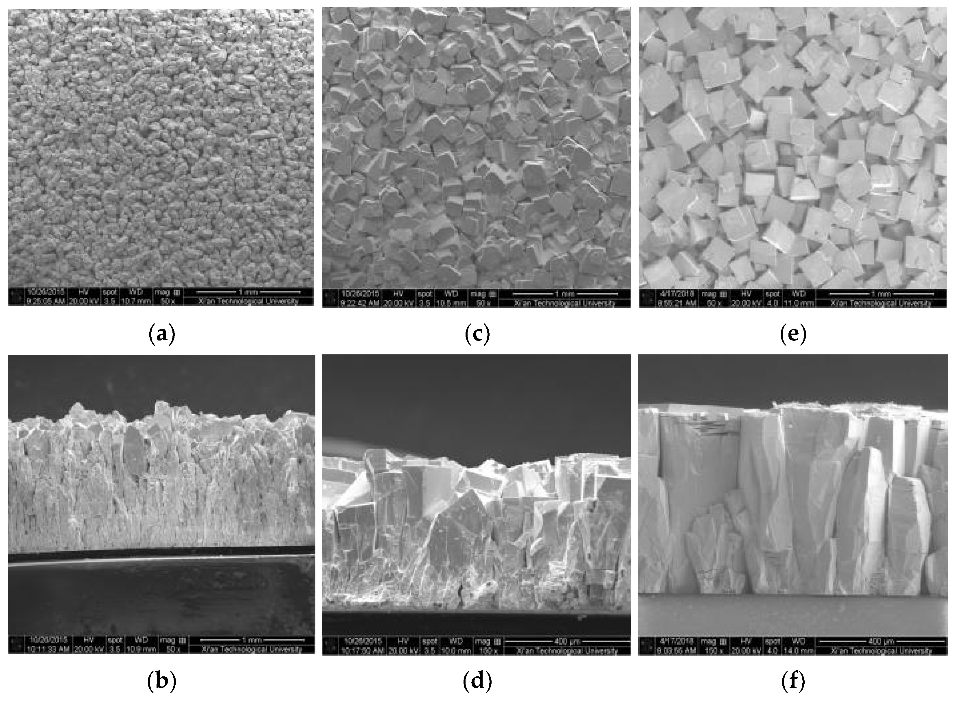
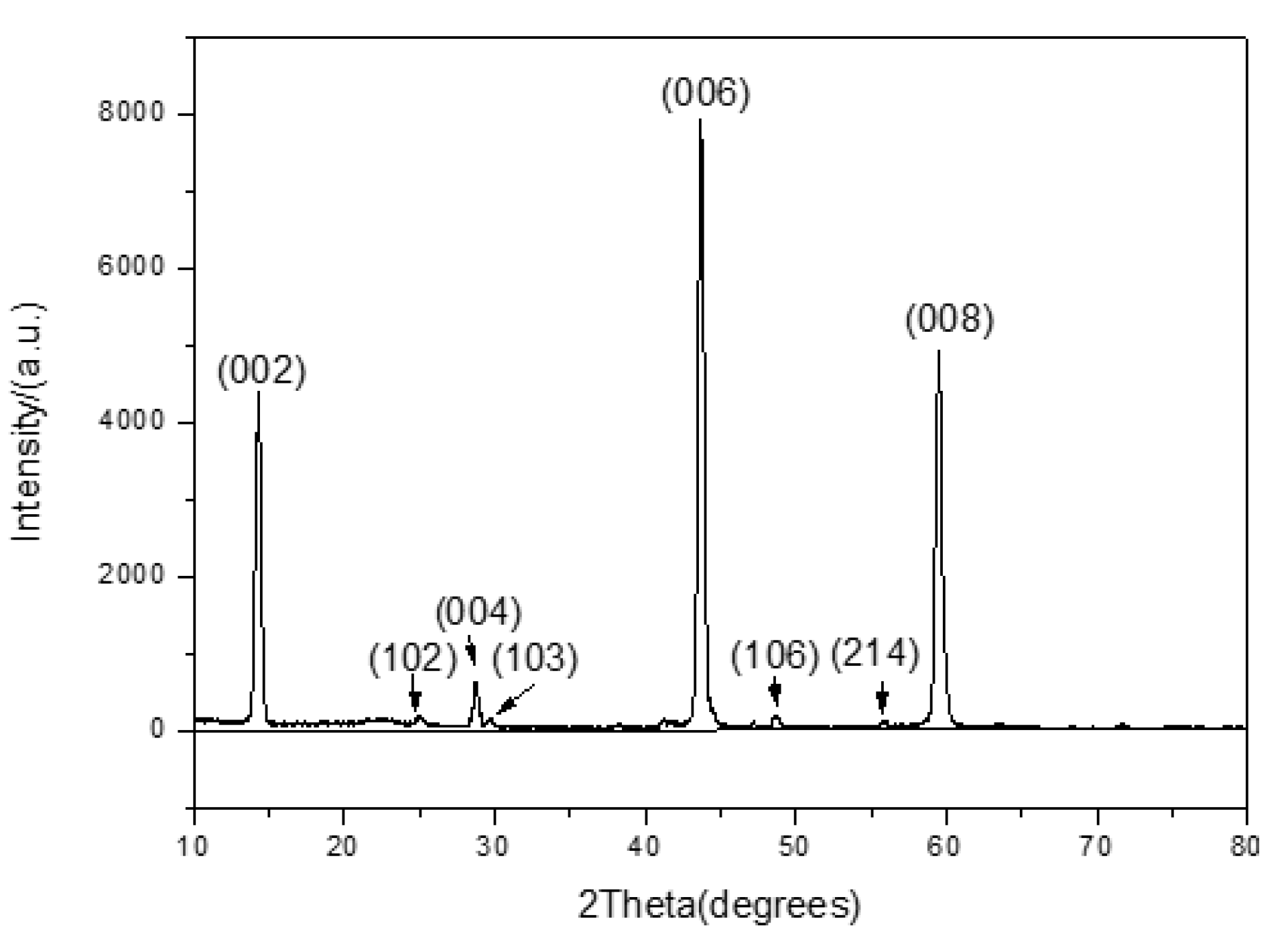
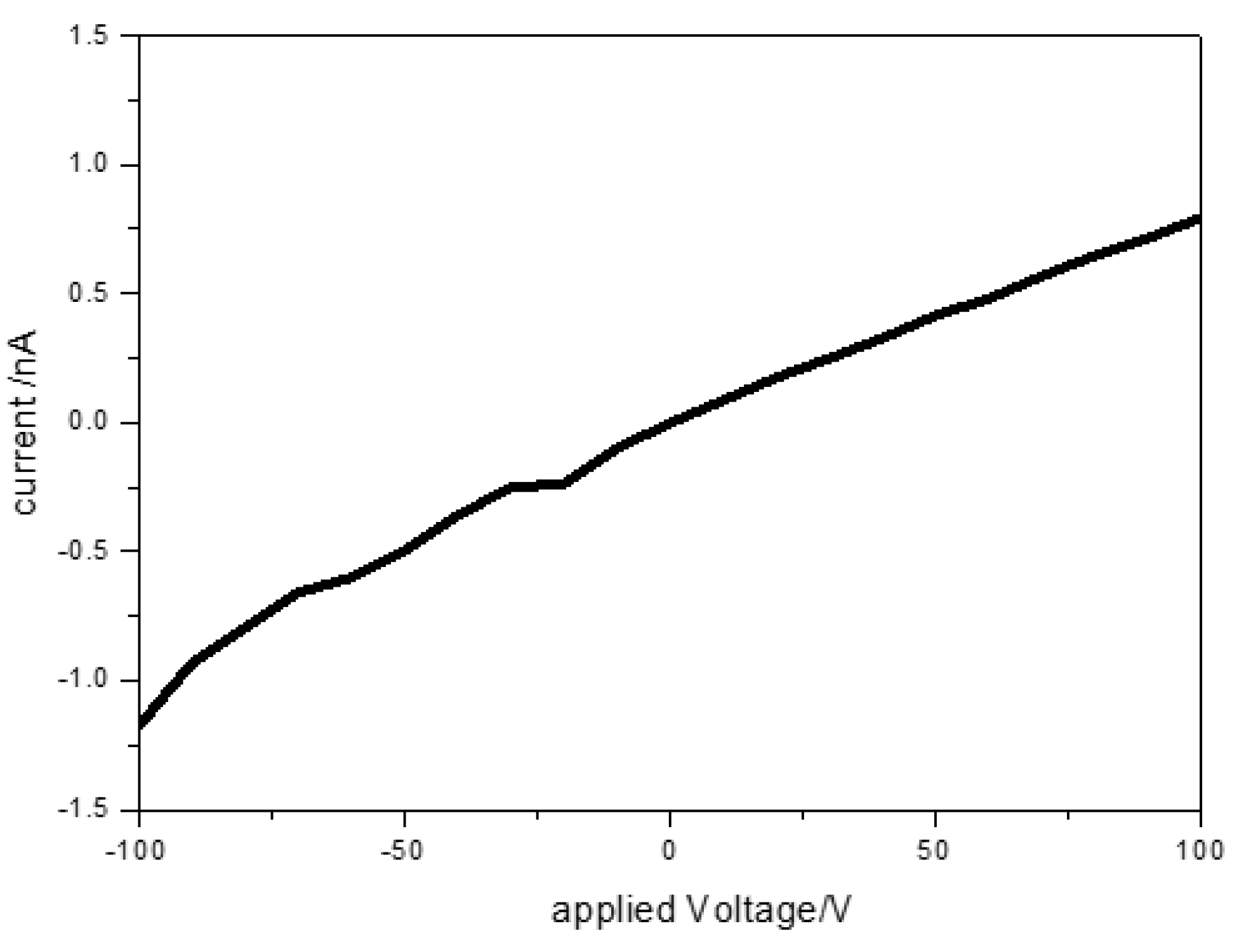
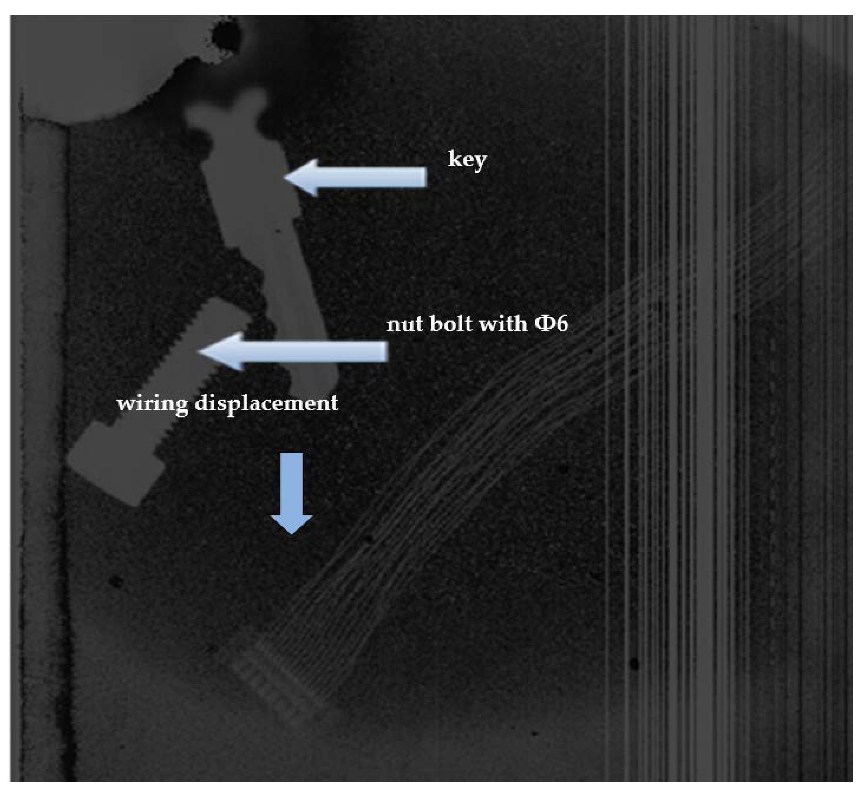
The synthesis method for high-purity raw material of HgI2 and growth furnace for films have been previously reported in detail in reference [12]. ITO and liquid crystal TFT with 170 cm2 in area were used as the substrate to grow the films, which was rinsed only in 18 MΩ de-ionized H2O. The whole growth cavity in the furnace was sealed below a vacuum of 6.6 × 10⁻³ Pa. The different depositing temperatures were 35, 40 and 45 °C, respectively. The source temperature was 100 °C. The growth period was set to be 2–2.5 h.
The texture of poly-films was studied by SHIMADZU 6000 X-ray diffraction meter with the X-ray wavelength of 1.5369 Å. The surface morphology of the films was examined using a FEI Quanta 400FScanning Electron Microscope. I–V characteristic of the as-grown film was measured by an Agilent 4155C IV instrument at room temperature. The digital X-ray imaging was obtained at Nuctech Company Limited, Beijing, China.

3. Results

The calculation method of growth temperature of some crystals in vapor has been provided [26]. Xu [27] optimized the growth temperature of HgI2 single crystal and poly-crystal films, as shown in Equation (1), and thought that the depositing temperature would increase with the increase of source temperature in a seal system. At the same time, the reasonable depositing temperature is 78~130 °C (0.3~0.5 Tm, Tm: Melting point, 259 °C for HgI2) for polycrystalline of HgI2, which is favorable to the formation of crystallography facets for grain, with complementary rectangular columnar structure [27]. Considering the match with readout matrix pixelation, the choice of temperature should be close to the lower limit for tiny grains.
T m i n 3 / 2 exp ( E S D K T m i n ) = 0.085 α C a 2 M 1 2 Δ P
Figure 1 gives the top and side of SEM photos of three different depositing temperature films with 170 cm2 area. For Figure 1a,b, the corresponding depositing temperature is 35 °C with 2.5 h in growth period. The grain size is less than 50 μm, and the thickness is about 1200 μm. Many grains agglomerate so the grain size cannot be distinctly observed in Figure 1a. Meanwhile, the films look like a stack of small HgI2 powder, viewing along the direction of growth from Figure 1b. Only on the top of the films, a few crystallographic planes are presented. Obviously, lower depositing temperature did not provide adequate energy for horizontal diffusion of sublimed HgI2 molecular on ITO, restricted the form of the crystallographic planes. Hence, the orientation of this film is not a very reasonable result, although detector assembled with this kind of film is available [12]. The grain size is about 120–180 μm with the thickness of 480–500 μm, as shown in Figure 1c,d, corresponding to 40 °C of depositing temperature and 2 h of growth period. Although the bottom of the films is also close to the stacking of the powders, the top part presents better crystalline morphology, which is an evident issue of raising the depositing temperature. The best effect was shown in Figure 1e,f for 45 °C of deposition, accompanied with 2 h in growth period. The films with grain size of 180–220 μm and thickness of 520 μm demonstrate a preferred microcrystal orientation, with complementary rectangular facets of the grains, and appropriate surface for electrode deposition. It is apparent that the result in Figure 1e,f is more adaptive for the necessity of assembling detector.
Figure 2 shows a HgI2-coated 13 × 13 cm2 on ITO with 45 °C of the depositing temperature and 100 °C of the source temperature, as well as 2 h growth period. It is obvious that red film distributes homogeneously. Figure 3 gives the XRD characteristic of the above film. The main (001) peak is very clear. According to the expressions ΣI(00l)/ΣI (hkl), the orientation along [001] was evaluated to be approximately 97.2%, which indicated a very excellent texture, while the texture of the film in Figure 1a,b could be estimated to close that of HgI2 powder according to the previous work [12].
The film’s growth on TFT corresponding to the best growth process, grown at 45 °C for 2 h was carried out. Au was sputtered onto the HgI2 poly-films as top electrode and TFT as back one, forming Au/HgI2/TFT contacts then. I–V curves of HgI2 films were measured using Agilent 4155C IV instrument at 25 °C. The testing result is shown in Figure 4. We can see the I–V curves present an approximate linear relation. The resistivity of the films was calculated to be 0.9 × 10¹² Ω⋅cm, which is coincident with the result published in reference [12] and also adequate for the need of detector-level films.
The imaging testing was carried out by the researcher in Nuctech Company Limited, Beijing. X-ray generator was set to 50 keV with 6 mA current. A key, a bolt with Φ 6 mm, and a wiring displacement were the objectives for imaging. Figure 5 shows planar X-ray images from 256 × 256 pixel HgI2 poly-films for the above subjects. The profile of the key was very clear, and about 1 mm of thread spacing of the bolt can be distinctly presented. Especially, 16 threads with 0.3 mm in diameter of a wiring displacement can be accounted distinctly. Obviously, the result was superior to the previous testing [12].
Considering the present and previous work [12], we thought that three different kinds of texture of the films were all adequate for detector assembling, and the third deposition process should be the best one. As shown in Figure 1f, the surface roughness of the film gets better with the growth temperature arising, which is in favor of electrode deposition, comparing the former two surface structures of the films grown. More importantly, the improvement of the orientation due to the increasing of depositing temperature is favorable to the sensitivity of the detector [25]. Therefore, the present results attribute to (001) orientation of the film and formation of the uniform electrical field. Nevertheless, the crack presents on the top of the grains in Figure 1f. It is well known that HgI2 is built from three-layer packages (I-Hg-I) with weak van der Walls bonding between adjacent planes of iodine atoms and perpendicular to the c-axis. This layered structure determines a high anisotropy for most of the properties. Isshiki [28] reported that HgI2 has indeed rather low thermal conductivity, 4 and 20 mW/cm⋅K, for the crystal direction parallel and perpendicular to the c-axis of HgI2 crystal. This is the reason why the crack occurs likely along the direction of parallel, other than perpendicular to (001) of crystal. The temperature of the growth surface arises due to the low thermal conductivity of HgI2 during crystal growth [29], leading to thermal stress on the top of the columnar grain and crack occurs. Meanwhile, the decline of supersaturation in vapor due to the increasing depositing temperature leads to the growth driving force decrease with time. Thereby, the thickness of the film attenuated to some extend with the elevation of depositing temperature in this work. Furthermore, the actual temperature on the surface of film would rise above one measured in the depositing field of ploy-films considering the thermal conductivity of crystal, which would be responsible for larger grain size shown in Figure 1c,e, especially the occurrence of cracks on the top of grain in Figure 1f. The above issues indicate the growth period would be reduced appropriately. Therefore, further study would focus on the growth of grain size less than 100 μm and the better orientation.

4. Conclusions

A large area HgI2 poly-films (170 cm2) was grown by PVD, applying for female breast examination. A 256 × 256 pixels X-ray image of a bolt, key, and a wiring displacement was distinctly presented with 50 keV with 6 mA current of X-ray generator. For HgI2 poly-films (170 cm2), films depositing at 35 °C look like the stack of HgI2 powder, present better crystalline morphology at 40 °C, and an excellent microcrystal orientation with 97.2% of [001]/[hkl] at 45 °C. The relationship between depositing temperature and crystallinity of grain shows that the higher depositing temperature, the better crystallinity and excellent preferred microcrystal orientation of grain, the larger the grain size. For matching readout matrix pixelation, the growth period of HgI2 poly-films poly-films would be reduced for reasonable grain size and preventing the formation of grain cracks.

Author Contributions

Conceptualization, L.Z. and G.X.; methodology, G.X. and Z.G.; investigation, L.Z. and G.X.; resources, L.Z. and Z.G.; data curation, M.Y., M.Z. and G.X.; validation, J.Z. and Y.W.; writing—original draft preparation, G.X. and Z.G.; project administration, G.X. and L.Z. All authors have read and agreed to the published version of the manuscript.

Funding

This research was funded by the National Natural Science Foundation of China, grant No. 52002304, National Natural Science Foundation of China, grant No. 11704301.

Institutional Review Board Statement

Not applicable.

Informed Consent Statement

Not applicable.

Data Availability Statement

Available on request.

Conflicts of Interest

The authors declare no conflict of interest.

References

  1. Cha, B.K.; Yang, K.; Cha, E.S.; Yong, S.M.; Heo, D.; Kim, R.K.; Jeon, S.; Seo, C.W.; Kim, C.R.; Ahn, B.T.; et al. Structural and electrical properties of polycrystalline CdTe films for direct X-ray imaging detectors. Nucl. Instr. Meth. A 2013, 731, 320–324. [Google Scholar] [CrossRef]
  2. Brus, V.V.; Solovan, M.N.; Maistruk, E.V.; Kozyarskii, I.P.; Maryanchuk, P.D.; Ulyanytsky, K.S.; Rappich, J. Specific features of the optical and electrical properties of polycrystalline CdTe films grown by the thermal evaporation method. Phy. Solid State 2014, 56, 1947–1951. [Google Scholar] [CrossRef]
  3. Zhu, X.-H.; Sun, H.; Yang, D.-Y.; Yang, J.; Li, X.; Gao, X.-Y. Fabrication and characterization of X-ray array detectors based on polycrystalline PbI2 th ick films. J. Mater. Sci. Mater. Electron. 2014, 25, 3337–3343. [Google Scholar]
  4. Zhu, X.H.; Sun, H.; Yang, D.Y.; Zheng, X.L. Growth, surface treatment and characterization of polycrystalline lead iodide thick films prepared using close space deposition technique. Nucl. Instr. Meth. A 2012, 691, 10–15. [Google Scholar] [CrossRef]
  5. Mulato, M.; Condeles, J.F.; Ugucioni, J.C. Comparative Study of HgI2, PbI2 and TlBr Films Aimed for Ionizing Radiation Detection in Medical Imaging. Mrs Online Proc. Libr. 2011, 1341, 145–150. [Google Scholar] [CrossRef]
  6. Fornaro, L.; Saucedo, E.; Mussio, L.; Gancharov, A.; Cuña, A. Bismuth tri-iodide polycrystalline films for digital X-ray radiography applications. IEEE Trans. Nucl. Sci. 2004, 51, 96–100. [Google Scholar] [CrossRef]
  7. Cuña, A.; Aguiar, I.; Gancharov, A.; Pérez, M.; Fornaro, L. Correlation between growth orientation and growth temperature for bismuth tri-iodide films. Cryst. Res. Technol. 2004, 39, 899–905. [Google Scholar] [CrossRef]
  8. Jiang, H.; Zhao, Q.; Antonuk, L.E.; Elmohri, Y.; Gupta, T. Development of active matrix flat panel imagers incorporating thin layers of polycrystalline HgI2 for mammographic x-ray imaging. Phys. Med. Biol. 2013, 58, 703–714. [Google Scholar] [CrossRef] [Green Version]
  9. Zentai, G.; Partain, L.; Pavlyuchkova, R.; Proano, C.; Virshup, G.; Melekhov, L.; Zuck, A.; Breen, B.N.; Dagan, O.; Vilensky, A.; et al. Mercuric iodide and lead iodide x-ray detectors for radiographic and fluoroscopic medical imaging. Proc. SPIE 2003, 5030, 77–91. [Google Scholar]
  10. Iwanczyk, J.S.; Patt, B.E.; Tull, C.R.; MacDonald, L.R.; Skinner, N.; Fornaro, L. HgI2 polycrystalline films for digital X-ray imagers. IEEE Trans. Nucl. Sci. 2002, 49, 160–164. [Google Scholar] [CrossRef]
  11. Iwanczyk, J.S.; Patt, B.E.; Tull, C.R.; MacDonald, L.R.; Skinner, N.; Hoffman, E.J.; Fornaro, L.; Mussio, L.; Saucedo, E.; Gancharov, A. Mercuric iodide polycrystalline films. Proc. SPIE 2001, 4508, 28–41. [Google Scholar]
  12. Xu, G.; Li, J.Y.; Nan, R.H.; Zhou, W.L.; Gu, Z.; Zhang, L.; Ma, X.M.; Cao, X.P. Large area HgI2 polycrystalline films for X-Ray imager. J. Optoelectron. Adv. Mater. 2016, 18, 842–846. [Google Scholar]
  13. Burger, A.; Nason, D.; Franks, L. Mercuric iodide in prospective. J. Cryst. Growth 2013, 379, 3–6. [Google Scholar] [CrossRef]
  14. Katsis, A.; Abel, E.; Pavlyuchkova, R.; Senapati, S.; Girdhani, S.; Parry, R. Abstract 3599: Implementation of a fully automated 3D foci counting algorithm to determine DNA damage in cells. Cancer Res. 2016, 76, 3599. [Google Scholar]
  15. El-Mohri, Y.; Antonuk, L.E.; Zhao, Q.; Su, Z.; Yamamoto, J.; Du, H.; Sawant, A.; Li, Y.; Wang, Y. TH-C-I-611-09: Development of Direct Detection Active Matrix Flat-Panel Imagers Employing Mercuric Iodide for Diagnostic Imaging. Med. Phys. 2005, 32, 2158. [Google Scholar] [CrossRef]
  16. Piechotka, M. Mercuric iodide for room temperature radiation detectors. Synthesis, purification, crystal growth and defect formation. Mater. Sci. Eng. 1997, 18, 1–98. [Google Scholar] [CrossRef]
  17. Van Scyoc, J.M.; James, R.B.; Burger, A.; Soria, E.; Perrino, C.; Cross, E.; Schieber, M.; Natarajan, M. Electrodrift purification of mercuric iodide for improved gamma-ray detector performance. Nucl. Instrum. Methods Phys. Res. Sect. A Accel. Spectrometers Detect. Assoc. Equip. 1996, 380, 36–41. [Google Scholar] [CrossRef]
  18. Schieber, M.; Zuck, A.; Braiman, M.; Melekhov, L.; Nissenbaum, J.; Turchetta, R.A.D.; Dulinski, W.; Husson, D.; Riester, J.L. Polycrystalline mercuric iodide detectors. Proc. SPIE 1997, 3115, 146–151. [Google Scholar]
  19. Schieber, M.; Zuck, A.; Melekhov, L.; Shatunovksy, R.; Hermon, H.; Turchetta, R.A.D. High-flux x-ray response of composite mercuric iodide detectors. Proc. SPIE 1999, 3768, 296–310. [Google Scholar]
  20. Ugucioni, J.C.; Netto, T.G.; Mulato, M. Mercuric iodide composite films using polyamide, polycarbonate and polystyrene fabricated by casting. Nucl. Instr. Meth. A 2010, 622, 157–163. [Google Scholar] [CrossRef]
  21. Xu, G.; Guo, Y.F.; Xi, Z.Z.; Gu, Z.; Zhang, L.; Yu, W.T.; Ma, X.M.; Li, B. Study on growth of large area mercuric iodide polycrystalline film and its X-ray Imaging. Proc. SPIE 2014, 9298, 91–97. [Google Scholar]
  22. Hartsough, N.E.; Iwanczyk, J.S.; Nygard, E.; Malakhov, N.; Barber, W.C.; Gandhi, T. Polycrystalline Mercuric Iodide Films on CMOS Readout Arrays. IEEE Trans. Nucl. Sci. 2009, 56, 1810–1816. [Google Scholar] [CrossRef] [Green Version]
  23. Schieber, M.; Hermon, H.; Zuck, A.; Vilensky, A.; Melekhov, L.; Shatunovsky, R.; Meerson, E.; Saado, Y.; Lukach, M.; Pinkhasyc, E.; et al. Thick films of X-ray polycrystalline mercuric iodide detectors. J. Cryst. Growth 2001, 225, 118–123. [Google Scholar] [CrossRef]
  24. Roy, U.N.; Cui, Y.; Wright, G.; Barnett, C.; Burger, A.; Franks, L.A.; Bell, Z.W. Polycrystalline mercuric iodide films: Deposition, properties, and detector performance. IEEE Trans. Nucl. Sci. 2002, 49, 1965–1967. [Google Scholar] [CrossRef]
  25. Fornaro, L. State of the art of the heavy metal iodides as photoconductors for digital imaging. J. Cryst. Growth 2013, 371, 155–162. [Google Scholar] [CrossRef]
  26. Dryburgh, P.M. The estimation of minimum growth temperature for crystals grown from the gas phas. J. Cryst. Growth 1988, 87, 397–407. [Google Scholar] [CrossRef]
  27. Xu, G.; Gu, Z.; Jian, Z.Y.; Xi, Z.Z.; Liu, C.X.; Zhang, G. Study on the lowest growth temperature of mercuric iodide. J. Synt. Growth 2012, 41, 1195–1199. [Google Scholar]
  28. Isshiki, M.; Piechotka, M.; Kaldis, E. Vapor growth kinetics of α-HgI2 crystals. J. Cryst.Growth 1990, 102, 344–348. [Google Scholar] [CrossRef]
  29. Zaletin, V.M.; Lyakh, N.V.; Ragozina, N.V. Stability of growth conditions and α-HgI2 crystal habit during growing by temperature oscillation method. Cryst. Res. Technol. 1985, 20, 307–312. [Google Scholar] [CrossRef]
Figure 1. Top (a,c,e) and side (b,d,f) SEM views of polyscrystalline HgI2 films.
Crystals 12 00032 g001
Figure 2. HgI2 -coated 13 × 13 cm2 on ITO.
Crystals 12 00032 g002
Figure 3. XRD pattern of polyscrystalline HgI2 film.
Crystals 12 00032 g003
Figure 4. I–V characteristic of polyscrystalline HgI2 film.
Crystals 12 00032 g004
Figure 5. Bolt, key, and wiring displacement image taken by X-ray Planar Images.
Crystals 12 00032 g005
Publisher’s Note: MDPI stays neutral with regard to jurisdictional claims in published maps and institutional affiliations.

