Article

Single-Step Fabrication and Characterization of Nanoscale Cu Thinfilms for Optoelectronic Applications

by
Hussein Alrobei
1,*,
Adnan Maqbool
2,
Muhammad Asif Hussain
2,
Rizwan Ahmed Malik
3,
Muhammad Ramzan Abdul Karim
4,
Ibrahim AlBaijan
1,
Azeem Hafiz
1 and
Muhammad Latif
5
1
Department of Mechanical Engineering, College of Engineering, Prince Sattam Bin Abdul Aziz University, AlKharj 16273, Saudi Arabia
2
Department of Metallurgical & Materials Engineering (MME), University of Engineering and Technology (UET), Lahore 54890, Pakistan
3
Department of Metallurgy and Materials Engineering, Faculty of Mechanical & Aeronautical Engineering, University of Engineering and Technology (UET), Taxila 47050, Pakistan
4
Faculty of Materials Science and Chemical Engineering, GIK Institute, Topi 23460, Pakistan
5
Center for Nanocellulose Future Composites, Department of Mechanical Engineering, Inha University, 100 Inha-Ro, Michuhol-Ku, Incheon 22212, Korea
*
Author to whom correspondence should be addressed.
Crystals 2022, 12(1), 62; https://doi.org/10.3390/cryst12010062
Submission received: 20 December 2021 / Accepted: 29 December 2021 / Published: 4 January 2022
(This article belongs to the Special Issue Synthesis, Characterization, and Properties of Nanomaterials)

Abstract

:
Nanostructured materials with optical transmittance with sufficient electrical conductivity are feasible for the transparent electrical devices and optoelectronic applications. Copper (Cu) possesses inherent superior electrical conductivity. Cu thin films on glass substrates provide the basic design understanding of the transparent electrodes for humidity sensors and solar cells applications. To understand the fundamental fabrication and electrical properties, a single-step facile fabrication approach was applied for Cu nanofilms through the DC sputtering method. Correlation of thickness of Cu nanofilms with optical and electrical properties was established. Parameters such as current, voltage, vacuum pressure, and time of coating were varied to develop different thickness of metal coating. Under optimized conditions of 10−1 torr vacuum, 1.45 KV voltage, and 4–6 min coating time, a conductive path is successfully established. A 1 min coated sample demonstrated resistance of 4000 ohm and conductance of a 6 min coated sample was raised to 56 m-mho. A higher surge of voltage assisted the production of relatively thick and uniform coatings with the crystallite size of 12 nm. The average coating thickness of 19.8 nm and roughness of 4.5 nm was obtained for a 5 min coated sample through AFM analysis. Further, it was observed that uniform nanostructured coating is essential to establish a mean free path of coated particles.

1. Introduction

In recent years, nanotechnology, a scientific revolution of the 21st century, has grown fast due to worldwide research and experimentation. For the advancement of this sector, nanoscale matter creation is of paramount importance [1,2]. Nanoparticles are particles with a minimum one dimension of 100 nm. Quantum dots, for example, may have no dimensions [3]. Nanoparticles reveal completely new and improved properties. The innovative and enriched features are mostly caused by size, distribution, and shape [4]. Nanoparticles have a large surface-to-volume ratio [5]. Nanomaterials are classified into three types based on their origin: natural, incidental, and engineered. Aside from the origin classification, there are metal, bimetallic, oxides, and other inorganic nanoparticles. There are four types of nanostructures: zero-, one-, two-, and three-dimensional structures. Due to their reduced dimensions, both quantum dots or quantum boxes have been referred to as zero dimensional [6,7].
Colloids, spherical nanoparticles, precipitates, fullerenes, and dendrimers are examples of nanostructures in three dimensions, which show all dimensions at the nanoscale [8]. Catalytic, magnetic [9], absorption, mechanical, sensitivity, and bioimaging properties, as well as applications in the agricultural, industrial, and medical domains, have all been revolutionized by these materials [10]. Nanomaterials have the potential to be used as lubricants. Paints and coatings, batteries, ceramics, clay, and fuel cells are only a few of the applications. Due to their wide use in a variety of disciplines, metal nanoparticles are extremely important [11].
Metal nanoparticles were discovered by Faraday, and Mie provided a quantitative explanation for their color. In addition to catalysis [12], metal nanoparticles are used in sensing, opto-electronics, and electrical engineering [13,14] because of their absorption sensitivity, medicinal, electrical [15], and catalytic properties based on shape, size, and structure. For their antibacterial properties against V staphylococcus aureus bacteria and Bacillus subtilis and for their applications in medicine and dental materials as well as sunscreen lotions, water treatment, and coatings, nanoparticles made of copper, gold, zinc, silver, magnesium, and titanium are of particular interest [8,9,10,11,12,13,14,15]. Their quality is dependent on their size, as well as the material in which they are embedded. It is possible to change the surroundings of nanoparticles in order to get the desired properties.
Metallics Copper nanoparticles are used in a variety of applications such as electronics, optics, and medicine, as well as the production of lubricants, conductive films, nanofluids, and antimicrobial agents [15,16,17,18,19,20]. Copper nanoparticles are preferred over silver nanoparticles because of their lower cost, relatively better chemical and physical stability, and ease of combining with polymers [21]. Smaller nanoparticles have a higher activity; however, they may form clusters, resulting in a loss of critical features [22]. Despite the extensive history of bulk copper “Cu” uses in numerous domains “e.g., optics, electronics, etc.”, however usage of nanoparticles is restricted because of inherent instability of Cu, “under atmospheric circumstances and susceptibility of oxidation”. Enhancement of Cu NPs sensitivity towards oxygen, water, and other chemical entities have prompted the development of more complex Cu-based NPs, such as core/shell Cu NPs or copper oxide systems.
Nanoparticles with high activity, stability, robustness, selectivity, and low cost pose the biggest challenge in developing catalytic NPs [23,24]. The main objective of this work is to develop the relationship of optical and electrical properties of Cu nanofilms, where the coating thickness is controlled through the combination of various parameters. A simple fabrication approach was chosen to prepare thin films of copper “Cu” with varying thicknesses that were deposited on the glass substrate using an Edwards Sputter Coater S150B and systematically studied the effects of vacuum pressure, voltage, and coating time on light transmittance, electrical resistance, and conductance of the prepared films.

2. Experimental Work

Using an Edwards Sputter Coater S150B, Crawley, West Sussex, RH10 2LW, UK a relatively easy fabrication process was chosen to prepare thin films copper “Cu” of various thicknesses that were coated on the glass substrate. The sputtering chamber settings “voltage and vacuum pressure” were also changed to see how these factors affected the optical and electrical properties of thin films. Light transmittance and electrical conductance used to characterize these thin films. The Digital LUX meter, Guangdong, China was used to calculate the light transmittance of thin coatings. Top view of the Cu coated samples was observed by a Stereozoom Microscope, “Nikon SMZ-2B, Tokyo, Japan”.
Prior to coating, acetone was utilized for ultrasonic cleaning of glass substrates for 10 min and rinsed in de-ionized water. In addition, the substrates are plasma cleaned for 5 min. To produce a homogeneous coating of different thicknesses, glass substrates were cut into 2 × 2 cm2 pieces and then cleaned as per standardized process. The glass substrates were impressed in acetone for 15 min in an ultrasonic bath, then rinsed with deionized water and dried.

2.1. Substrate Cleaning

Glass substrates were used as substrate for thin films. Cleaning of the glass substrates was done to remove dust and contamination from the surface of the substrates, to avoid any impurity in the thin films. To clean the substrate, sonication was done in ethanol for 15 min.

2.2. Sputtering of Copper

Copper target, argon “Ar” gas, and glass substrate were used in this experiment. Copper thin films of three different categories were deposited by using “Edwards Sputter Coater S150B”, by varying the conditions “Voltage & Vacuum pressure” of the sputtering chamber. The constant parameters for sputtering were pressure of “Ar” gas from cylinder = 0.5 barr, vacuum before coating = 10−2 torr and time of coating = 1–5 min. The coating thickness is controlled through the combination of various parameters (coating as a function of deposition time is about 10–15 nm/min at given conditions, according to standard machine manual). The varying parameters for three different categories of coating are summarized in the Table 1.

2.3. Light Transmittance of Copper Nano-Films

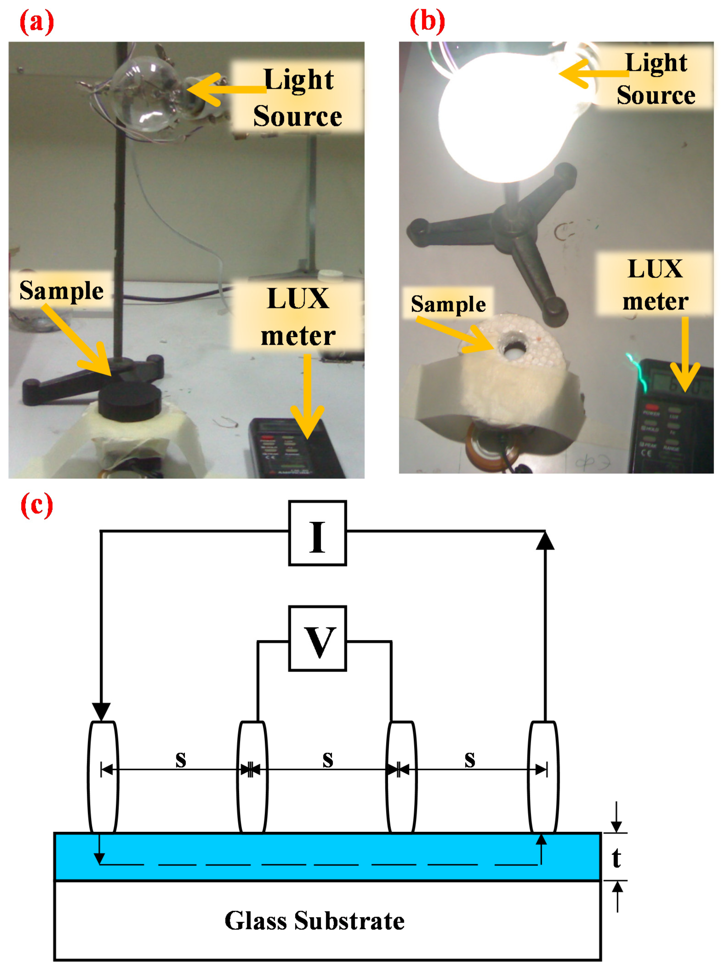
The percentage of light transmittance was calculated. In the first step, the intensity of the light source was measured. The light intensity was then measured by placing a glass substrate and coated samples between the light source and the lux meter. It is important to realize that the visual inspection is first part of the characterization where through naked eye one can see the uniform or uneven covering of sputter coated films. However, the thickness was measured through detailed atomic force microscope (AFM) and discussed in the later part. Figure 1a depicts the configuration utilized in the current study and Figure 1b demonstrate the sample after copper coating while Figure 1c explains the mechanism of the coating involved in the current study.
The data obtained by the Lux meter are given in Table 2.

2.4. Measurement of Conductance of Copper Nanofilms

The I–V characteristic of the thin films of category-3 was measured by using four probe method. In the experiment current was kept constant and corresponding voltage produced was measured by using the source meter. The schematic diagram of the experimental set up is shown in following Figure 2.
Resistance and conductance of thin films were assessed by measuring their I–V characteristics. As
V = IR “Ohm’s law”
Therefore,
Resistance “R” = V/I “ohm”
Conductance “G” = 1/R “mho”
The conditions applied during the experiment and data obtained from it are given in Table 3.
Due to non-uniform and uneven coatings of category 1 and 2, it was not possible to measure the I–V characteristics of these thin films. So, we were not able to calculate the electrical resistance and conductance also.
X-ray diffraction “XRD” analyses was performed by “Model PW 3710, Philips Panalytical X-pert, Almelo, The Netherlands” with Cu as Kα radiations and Scherrer’s formula was used to estimate the crystallite size. Atomic force microscope (AFM) analysis was carried out to measure the coating thickness and surface roughness of the coated film. FlexAFM C3000i controller by Nanosurf (Gräubernstrasse, Liestal, Switzerland) was utilized for the analysis.

3. Results and Discussions

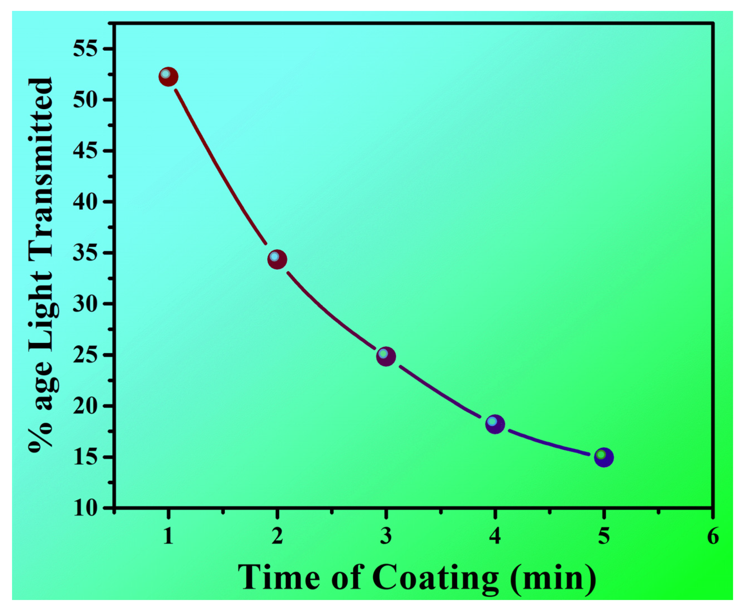
Figure 3 shows a graphical illustration of the relationship between coating time and percentage light intensity transmitted. The observed percentage of light transmitted at 1 min is 53 percent, as can be seen. However, as time passes, the percentage of light transmittance decreases. The percentage of light transmitted through the coated samples decreases as the coating duration rises, as shown in this graph. This demonstrates that the coating thickness grows as the coating duration increases.
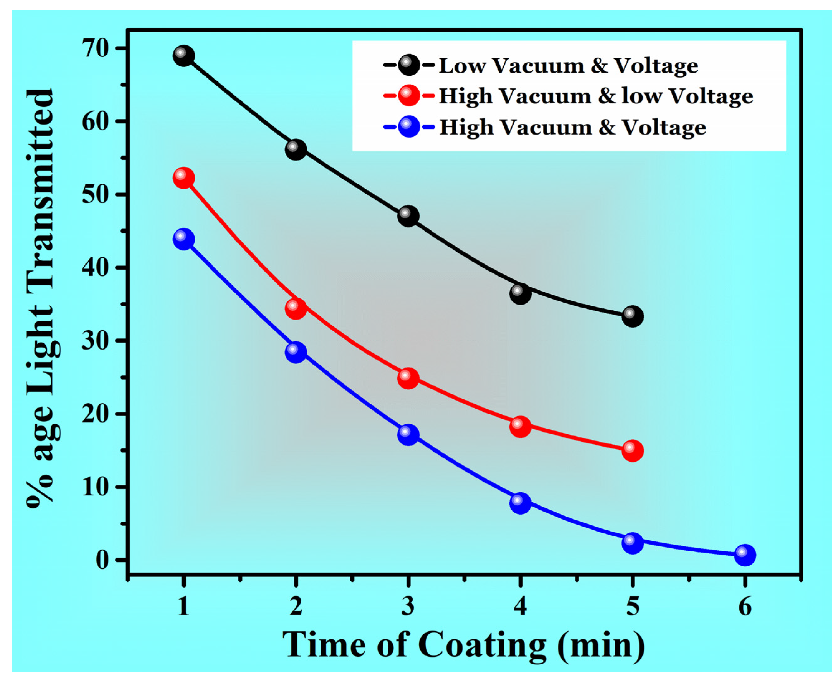
At constant voltage of 0.9 KV, Figure 4 depicts how the proportion of light intensity transmitted through samples changes as the vacuum pressure changes. At low vacuum pressure, the proportion of light intensity transmitted is higher as compared to proportion of light intensity transmitted at high vacuum pressure. When the results obtained at low vacuum pressure “2 torr” and high vacuum pressure “10−1 torr” at constant voltage “0.9 KV” are compared, it is obvious that the coating at high vacuum pressure is superior to the coating at low vacuum pressure, as shown in Figure 4. This is because the mean free path of the coated particles increases at high vacuum pressure.
At constant high vacuum pressure of 10−1 torr, Figure 5 depicted the effect of applied voltage on the percentage of light transmittance as a function of time. At 1 min, the percentage of light transferred at high applied voltage is 44 percent, whereas at low applied voltage, the percentage of light transmitted is 53 percent. These findings indicate that at high voltage, a more uniform coating is obtained. This is demonstrated in Figure 5 by comparing the curves obtained at low voltage “0.9 KV” and high voltage “1.45 KV” at constant high vacuum pressure “10−1 torr”.
Figure 6 depicted the percentage light transmittance as a function of voltage at various time intervals. It is clear from this graph that the light transmittance of the coating obtained after 6 min is almost zero. The substrate coated for 12 min at high voltage “1.45 KV” and high vacuum pressure “10−1 torr” is almost opaque even at the source intensity of 700 Lux. When all three coating categories are compared, it is obvious from Figure 6 that the coating at high vacuum and high voltage is the best of all.
The number of electrons per unit volume, the electric charge -e “−1.6010−19 C”, and the electron drift velocity Vd all affect the electron flow in a metallic film subjected to potential difference [25]. The current density “J” is calculated using the following formula:
Current density “J” = neVd
When the coating thickness is increased, the number of charge carriers “-e” increases as well. The conductance of the coatings will increase as the thickness of the coating grows due to an increase in current density. The data acquired for the coatings exhibit the same pattern as that presented in Figure 7.
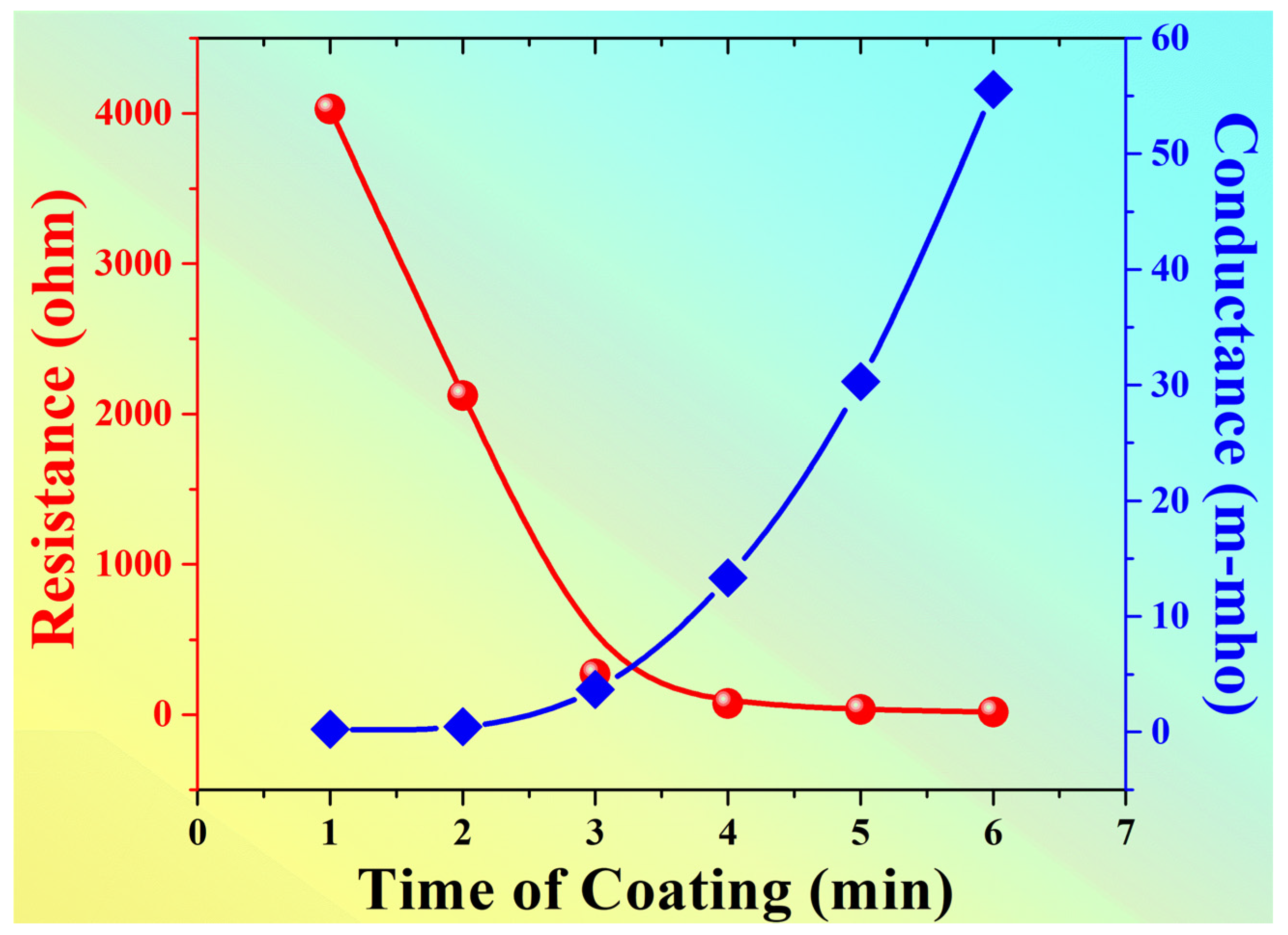
Figure 8 depicts the relationship between coating resistance and conductance. As illustrated in Figure 8, this is further confirmed by comparing the conductance of the coatings with their resistance. The maximum resistance of 4000 ohm was obtained for a 1 min coated sample, while the conductance of a 6 min coated sample was surged to 56 m-mho. The conductance of the samples increased over time, indicating that the coating thickness is directly proportional to the conductance and eventually inversely proportional to the resistance of the produced films.
XRD analysis is used to determine the crystallite size of thin films and to ensure that no oxide or other compound forms during the sputtering process. Figure 9 shows the results of the XRD scan. The XRD pattern is in good agreement with previous study [26]. The XRD analyses indicated the presence of single Cu crystalline phase and absence of copper oxide phase, “within the detection limit of XRD equipment”. The existence of small Cu nanocrystals can be suggested by broadening of XRD peaks [26,27].
The Scherrer’s formula was applied to measure the crytallite size, which is as follows:
t = K λ B Cos   θ B
The size of the crystallite formed is “t” = 12 nm that confirms the generation of nanoscale crystals in the deposited films, according to the findings. As a result, by adjusting the deposition conditions, nanoscale crystalline can be produced in the easy and reproducible sputtering process. This work reported the relationship of optical and electrical properties of Cu nanofilms, where the coating thickness is controlled through the combination of various parameters [28,29,30,31].
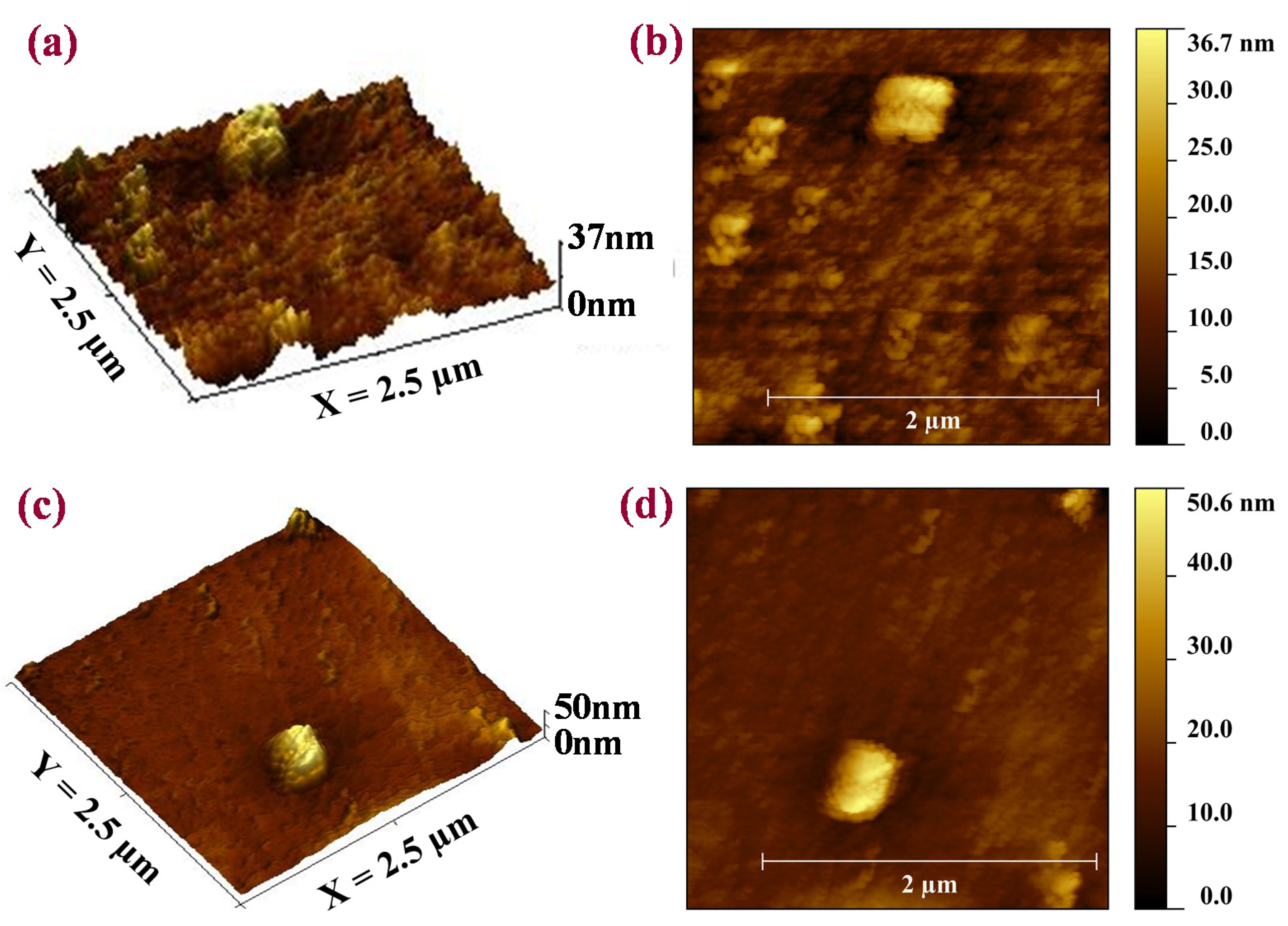
AFM analysis was carried out to evaluate the surface topography of the Cu-coated film. Figure 10 demonstrates the AFM analysis of the Cu film of category-1 with 5 min sputtering time. Overall uniform coating of Cu was obtained by using the given parameters, and AFM images suggest the average coating thickness is 19.8 nm, as shown in Table 4. Figure 10a,b shows the uniform distribution of Cu particles throughout the surface of the scanned surface where the size of maximum film thickness is ~37 nm. The Cu particles are connected with each other and the anticipated long mean-free path is well developed for enhanced conduction. Figure 10c,d reveals the selected area of individual Cu island, which has grown to a maximum height of ~50 nm. Despite the formation of individual islands, the average roughness behavior remained similar, as summarized in Table 4.

4. Conclusions

In this work, single-step Cu nanofilms were generated by using the simple and reproducible DC sputtering method. Parametric variation was carried out, and correlation of thickness of Cu nanofilms was established with optical and electrical properties. The non-uniform coatings were attained in categories 1 and 2, where the vacuum and voltage were low. The significant porosity and discontinuity in these films were demonstrated by higher values of the percentage of light transmitted, and inconsistent and unreliable I–V characteristics. Under optimized conditions of 10−1 torr vacuum, 1.45 KV voltage, and 4–6 min coating time, a conductive path was successfully established. The maximum resistance of 4000 ohm was obtained for a 1 min coated sample, while the conductance of a 6 min coated sample surged to 56 m-mho. Coatings were relatively thick and uniform with a crystallite size of 12 nm in category 3, where vacuum pressure and voltage were rather high. The average coating thickness of 19.8 nm and roughness of 4.5 nm was obtained for a 5 min coated sample through AFM analysis. Further, it is suggested that for the production of thin and uniform coatings, the pressure and voltage must be high enough to give the coating particles a long mean-free path for enhanced conduction.

Author Contributions

Conceptualization, M.A.H. Data curation, A.H.; methodology, M.A.H.; software, A.M. and R.A.M.; formal analysis, A.M., R.A.M. and I.A.; investigation, M.A.H., R.A.M., A.M. and M.R.A.K.; writing—original draft preparation, H.A., M.A.H. and R.A.M.; writing—review and editing, H.A., A.M., R.A.M. and M.L.; supervision, H.A.; project administration, H.A.; funding acquisition, H.A. All authors have read and agreed to the published version of the manuscript.

Funding

This research received no external funding.

Institutional Review Board Statement

Not applicable.

Informed Consent Statement

Not applicable.

Data Availability Statement

The data that support the findings of this study is included in the article.

Acknowledgments

This study was supported by the Deanship of Scientific Research at Prince Sattam Bin Abdulaziz University under research project no. 2020/01/17063.

Conflicts of Interest

The authors declare no conflict of interest.

References

  1. Sivakumar, J.; Premkumar, C.; Santhanam, P.; Saraswathi, N. Biosynthesis of silver nanoparticles using Calotropis gigantean leaf. Afr. J. Basic Appl. Sci. 2011, 3, 265–270. [Google Scholar]
  2. Din, M.I.; Rehan, R. Synthesis, Characterization, and Applications of Copper Nanoparticles. Anal. Lett. 2017, 50, 50–62. [Google Scholar] [CrossRef]
  3. Hudlikar, M.; Joglekar, S.; Dhaygude, M.; Kodam, K. Latex-mediated synthesis of ZnS nanoparticles: Green synthesis approach. J. Nanoparticle Res. 2012, 14, 1–6. [Google Scholar] [CrossRef]
  4. Singh, R.P.; Shukla, V.K.; Yadav, R.S.; Sharma, P.K.; Singh, P.K.; Pandey, A.C. Biological approach of zinc oxide nanoparticles formation and its characterization. Adv. Mater. Lett. 2011, 2, 313–317. [Google Scholar] [CrossRef]
  5. Awwad, A.M.; Salem, N.M.; Abdeen, A.O. Biosynthesis of Silver Nanoparticles using Olea europaea Leaves Extract and its Antibacterial Activity. Nanosci. Nanotechnol. 2012, 2, 164–170. [Google Scholar] [CrossRef] [Green Version]
  6. Reed, M.A.; Randall, J.N.; Aggarwal, R.J.; Matyi, R.J.; Moore, T.M.; Wetsel, A.E. Observation of discrete electronic states in a zero-dimensional semiconductor nanostructure. Phys. Rev. Lett. 1988, 60, 535–537. [Google Scholar] [CrossRef]
  7. Takagahara, T. Effects of dielectric confinement and electron-hole exchange interaction on excitonic states in semiconductor quantum dots. Phys. Rev. B 1993, 47, 4569–4584. [Google Scholar] [CrossRef] [PubMed]
  8. Zheng, N.; Fan, J.; Stucky, G.D. One-Step One-Phase Synthesis of Monodisperse Noble-Metallic Nanoparticles and Their Colloidal Crystals. J. Am. Chem. Soc. 2006, 128, 6550–6551. [Google Scholar] [CrossRef]
  9. Easom, K.A.; Klabunde, K.J.; Sorensen, C.; Hadjipanayis, G.C. Nanoscale magnetic particles. New methods to surface protected metallic and immiscible bimetallic clusters/particles. Polyhedron 1994, 13, 1197–1223. [Google Scholar] [CrossRef]
  10. Wu, W.; Shen, J.; Banerjee, P.; Zhou, S. Core–shell hybrid nanogels for integration of optical temperature-sensing, targeted tumor cell imaging, and combined chemo-photothermal treatment. Biomaterials 2010, 31, 7555–7566. [Google Scholar] [CrossRef]
  11. Gawande, M.B.; Goswami, A.; Felpin, F.-X.; Asefa, T.; Huang, X.; Silva, R.; Zou, X.; Zboril, R.; Varma, R.S. Cu and Cu-Based Nanoparticles: Synthesis and Applications in Catalysis. Chem. Rev. 2016, 116, 3722–3811. [Google Scholar] [CrossRef] [Green Version]
  12. Wunder, S.; Polzer, F.; Lu, Y.; Mei, Y.; Ballauff, M. Kinetic Analysis of Catalytic Reduction of 4-Nitrophenol by Metallic Nanoparticles Immobilized in Spherical Polyelectrolyte Brushes. J. Phys. Chem. C 2010, 114, 8814–8820. [Google Scholar] [CrossRef]
  13. Homola, J.; Yee, S.S.; Gauglitz, G. Surface plasmon resonance sensors: Review. Sens. Actuators B Chem. 1999, 54, 3–15. [Google Scholar] [CrossRef]
  14. Taton, T.A.; Mirkin, C.A.; Letsinger, R.L. Scanometric DNA Array Detection with Nanoparticle Probes. Science 2000, 289, 1757–1760. [Google Scholar] [CrossRef] [Green Version]
  15. Sun, S.; Murray, C.B.; Weller, D.; Folks, L.; Moser, A. Monodisperse FePt Nanoparticles and Ferromagnetic FePt Nanocrystal Superlattices. Science 2000, 287, 1989–1992. [Google Scholar] [CrossRef]
  16. Glavee, G.N.; Klabunde, K.J.; Sorensen, C.; Hadjipanayis, G.C. Borohydride reduction of cobalt ions in water. Chemistry leading to nanoscale metal, boride, or borate particles. Langmuir 1993, 9, 162–169. [Google Scholar] [CrossRef]
  17. Liz-Marzán, L.M.; Touriño, I.L. Reduction and Stabilization of Silver Nanoparticles in Ethanol by Nonionic Surfactants. Langmuir 1996, 12, 3585–3589. [Google Scholar] [CrossRef]
  18. Yu, Y.Y.; Chang, S.-S.; Lee, C.-L.; Wang, C.R.C. Gold Nanorods: Electrochemical Synthesis and Optical Properties. J. Phys. Chem. B 1997, 101, 6661–6664. [Google Scholar] [CrossRef]
  19. Maksoud, M.I.A.A.; Fahim, R.A.; Shalan, A.E.; Elkodous, M.A.; Olojede, S.O.; Osman, A.I.; Farrell, C.; Al-Muhtaseb, A.H.; Awed, A.S.; Ashour, A.H.; et al. Advanced materials and technologies for supercapacitors used in energy conversion and storage: A review. Environ. Chem. Lett. 2021, 19, 375–439. [Google Scholar] [CrossRef]
  20. Sanad, M.F.; Shalan, A.E.; Abdellatif, S.O.; Abu Serea, E.S.; Adly, M.S.; Ahsan, A. Thermoelectric Energy Harvesters: A Review of Recent Developments in Materials and Devices for Different Potential Applications. Top. Curr. Chem. 2020, 378, 1–43. [Google Scholar] [CrossRef] [PubMed]
  21. Mallik, K.; Mandal, M.; Pradhan, A.N.; Pal, T. Seed Mediated Formation of Bimetallic Nanoparticles by UV Irradiation: A Photochemical Approach for the Preparation of “Core−Shell” Type Structures. Nano Lett. 2001, 1, 319–322. [Google Scholar] [CrossRef]
  22. Tolaymat, T.M.; El Badawy, A.M.; Genaidy, A.; Scheckel, K.; Luxton, T.P.; Suidan, M. An evidence-based environmental perspective of manufactured silver nanoparticle in syntheses and applications: A systematic review and critical appraisal of peer-reviewed scientific papers. Sci. Total. Environ. 2010, 408, 999–1006. [Google Scholar] [CrossRef] [Green Version]
  23. Somorjai, G.A.; Park, J.Y. Molecular Factors of Catalytic Selectivity. Angew. Chem. Int. Ed. 2008, 47, 9212–9228. [Google Scholar] [CrossRef] [PubMed]
  24. Ben Aissa, M.A.; Tremblay, B.; Andrieux-Ledier, A.; Maisonhaute, E.; Raouafi, N.; Courty, A. Copper nanoparticles of well-controlled size and shape: A new advance in synthesis and self-organization. Nanoscale 2015, 7, 3189–3195. [Google Scholar] [CrossRef] [Green Version]
  25. Smith, W.F. Principles of Materials Science and Engineering; Mc-Graw Hill Series: New York, NY, USA, 1999. [Google Scholar]
  26. Khan, A.; Rashid, A.; Younas, R.; Chong, R. A chemical reduction approach to the synthesis of copper nanoparticles. Int. Nano Lett. 2016, 6, 21–26. [Google Scholar] [CrossRef] [Green Version]
  27. Murugadoss, G.; Rajamannan, B.; Madhusudhanan, U. Synthesis and characterization of water-soluble ZnS: Mn2+ nanocrystals. Chalcogenide Lett. 2009, 6, 197–201. [Google Scholar]
  28. Hussain, M.A.; Choi, E.J.; Maqbool, A.; Atif, M.; Zeb, H.; Yeo, J.; Yu, J.-A.; Cho, Y.-H.; Noh, M.; Kim, J.W. An efficient hydration of nitriles with ruthenium-supported heterogeneous catalyst in water under moderate conditions. J. Ind. Eng. Chem. 2021, 99, 187–195. [Google Scholar] [CrossRef]
  29. Maqbool, A.; Hussain, M.A.; Khalid, F.A.; Bakhsh, N.; Hussain, A.; Kim, M.H. Mechanical characterization of copper coated carbon nanotubes reinforced aluminum matrix composites. Mater. Charact. 2013, 86, 39–48. [Google Scholar] [CrossRef]
  30. Karimov, K.S.; Khalid, F.A.; Chani, M.; Mateen, A.; Hussain, M.A.; Maqbool, A.; Ahn, J. Carbon nanotubes based flexible temperature sensors. Optoelectron. Adv. Mater. Rapid Commun. 2012, 6, 194–196. [Google Scholar]
  31. Karimov, K.S.; Chani, M.T.S.; Khalid, F.A. Carbon nanotubes film based temperature sensors. Phys. E Low Dimens. Syst. Nanostructures 2011, 43, 1701–1703. [Google Scholar] [CrossRef]
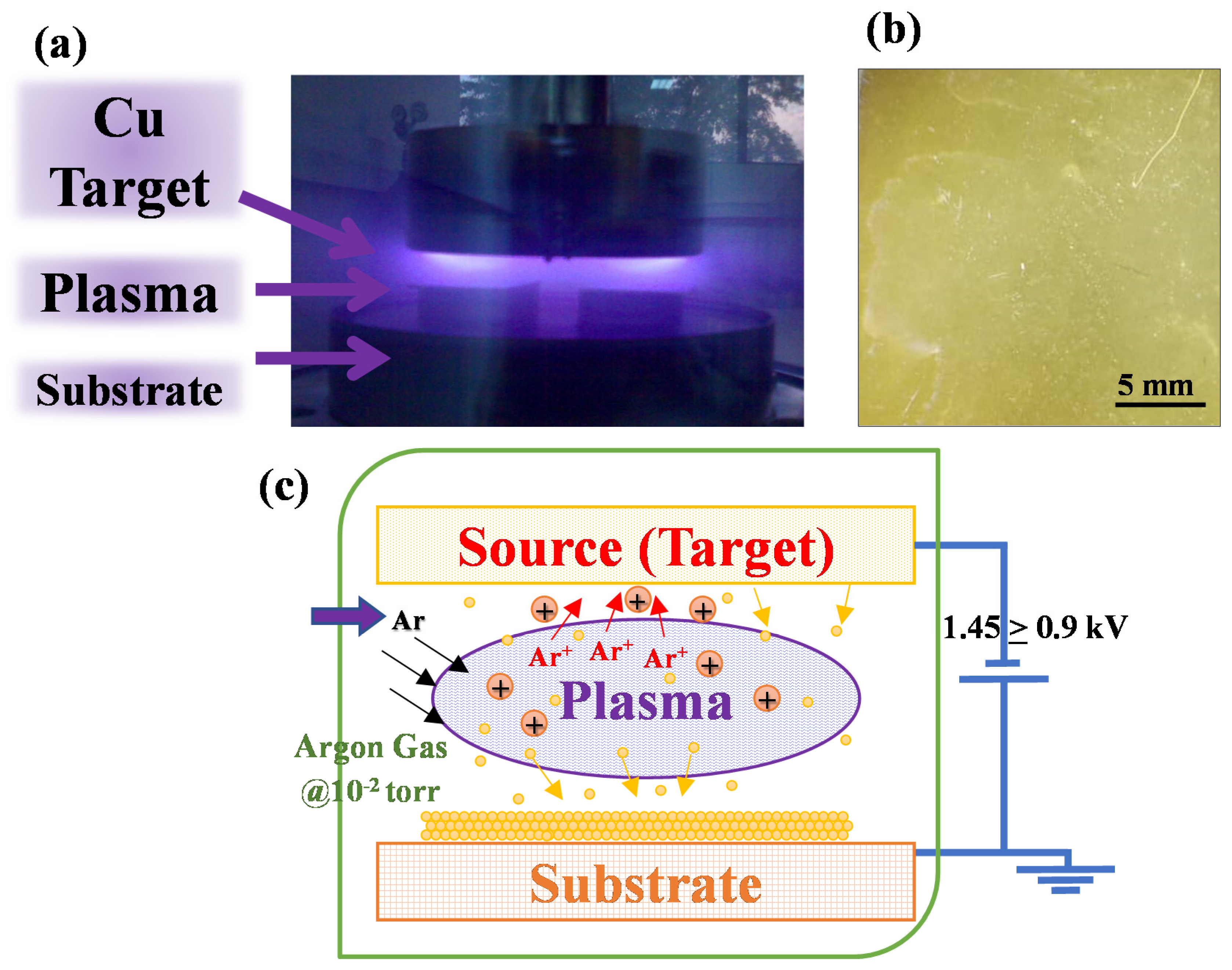
Figure 1. (a) Plasma assisted coating in the sputtering chamber, (b) Stereoscopic optical image of Cu coated sample, (c) Schematic representation of the sputtering phenomenon.
Crystals 12 00062 g001
Figure 2. (a) Side view of setup to measure the transmitted Light intensity, (b) Top view with light source turned on, and (c) Schematic of Four probe system.
Crystals 12 00062 g002
Figure 3. Relationship between coating time and % age light.
Crystals 12 00062 g003
Figure 4. Comparison of Sputtered Coatings at Different Vacuum.
Crystals 12 00062 g004
Figure 5. Comparison of Sputtered Coatings at Different Voltages.
Crystals 12 00062 g005
Figure 6. Comparison of Sputtered Coatings under Different Conditions.
Crystals 12 00062 g006
Figure 7. Relationship between coating time and conductance.
Crystals 12 00062 g007
Figure 8. Relationship between Resistance and Conductance of the Coatings.
Crystals 12 00062 g008
Figure 9. (a) X-ray diffraction analysis of synthesized nanofilms, (b) FWHM of the Cu peak.
Crystals 12 00062 g009
Figure 10. (a,b) AFM images of densely Cu-coated film showing the uniform film thickness, (c,d) AFM images of selected area of the Cu deposited island showing the maximum film thickness.
Crystals 12 00062 g010
Table 1. Varying conditions for different categories of coatings.
Category No.Pressure during Coating “torr”Voltage “K-Volt”Current “mA”
120.925
210−10.925
310−11.4513
Table 2. Percentage of light transmitted through thin films.
Coating Time “min”12345
Percentage Light Intensity TransmittedCategory 168.9356.152.2736.433.3
Category 252.2434.3331.3418.1814.93
Category 343.8728.3917.17.742.26
Initial intensity of light source = 150 Lux. Light intensity transmitted through substrate = 145 Lux. Percentage of light transmitted through sample = Light   tarnsmitted   through   film Light   transmitted   through   substrate × 100 .
Table 3. Electrical properties of thin films of category 3.
Time of Coating “min”12345
Voltage “volt”40.2621.232.710.750.33
Resistance “Ω”402621232717533
Conductance “m-mho”0.2480.4713.6913.3330.30
Experiment performed at room temperature. Current supplied = 10 mA.
Table 4. Statistical quantities of AFM analysis for Cu film for 5 min sample.
Sr. No.Average Thickness “nm”Average Roughness “nm”Maximum Island Thickness “nm”
Area 119.84.336.6
Area 220.74.550.1
Publisher’s Note: MDPI stays neutral with regard to jurisdictional claims in published maps and institutional affiliations.