Article

Improved Optoelectronic Properties of Nanostructured Eu Doped Bi2S3 Thin Films for the Detection of UV Light

1
Advanced Functional Materials & Optoelectronics Laboratory, Department of Physics, College of Science, King Khalid University, P.O. Box 9004, Abha 61413, Saudi Arabia
2
University Center for Research & Development (UCRD), Chandigarh University, Mohali 140413, India
3
Department of Physics, College of Science, Princess Nourah bint Abdulrahman University, P.O. Box 84428, Riyadh 11671, Saudi Arabia
4
Department of Materials Science and Engineering and Chemical Engineering, Universidad Carlos III de Madrid, 28911 Madrid, Spain
5
Department of Chemistry, College of Science, King Saud University, P.O. Box 2455, Riyadh 11451, Saudi Arabia
*
Author to whom correspondence should be addressed.
Crystals 2022, 12(10), 1329; https://doi.org/10.3390/cryst12101329
Submission received: 27 August 2022 / Revised: 14 September 2022 / Accepted: 16 September 2022 / Published: 20 September 2022

Abstract

:
Due to a suitable band gap and high light absorption behavior, Bi2S3 is showing major success in photo-to-current conversion applications. In this current work, the authors used a low-cost nebulizer spray pyrolysis method to create nano-sized pure and unique Eu contents (1–5 wt.%)-loaded Bi2S3 thin layers by taking bismuth nitrate and thiourea as the source materials. The parent and Eu doped Bi2S3 thin films, deposited on a well-cleaned glass substrate at 350 °C, were analyzed using a variety of characterization approaches, including FESEM, EDS, XRD, PL, UV-Vis, and I-V, to describe the morphologies, compositions, crystallinity, defect states, band gap, and photodetection capability, respectively. The X-ray diffraction outcomes confirmed an orthorhombic polycrystalline structure for all Eu concentrations, and they were highly oriented along the (130) plane. Incorporation of Eu into the host matrix improves the intensity of all the peaks, and the crystallite size (25 nm) was found to be highest for the 3% Eu doped Bi2S3 thin film. The formation of a nanowire-like morphology was confirmed thorough field emission electron microscopy analysis, which is preferred for photo detectors. Upon excitation at 325 nm, grown pure and Eu doped Bi2S3 thin films indicated five emission peaks at 387, 418, 439, 480, and 523 nm, respectively. All the films showed significant absorption in the UV region, and importantly, a narrowing of the band gap is seen from 2.29 to 2.17 eV. Finally, the current-voltage characteristics of the pure and Eu doped Bi2S3 thin films were tested using silver contacts as electrodes. The results showed that the 3% Eu doped Bi2S3 sample showed a higher UV photocurrent characteristic, with high specific detectivity (1.82 × 10¹⁰ Jones), photoresponsivity (3.88 × 10⁻¹ AW−1), external quantum efficiency (125%), and rapid photo response, as well as a recovery speed of 0.3 s and 0.4 s, due to the effective light absorption and photocarrier generation. We believe that our study may provide a cost-effective approach for UV photosensor applications.

1. Introduction

In recent years, modern academic and industrial researchers have expended tremendous research efforts for technological advancement in the fields of electronics and optoelectronics due to their excellent applications. There is no doubt that photosensors or photodetectors are the lifeblood of the optoelectronic industry, as they converts absorbed photons into electrical signals via electron–hole pair creation. Recently, the research hotspot has turned to finding low cost as well as non-toxic photosensing semiconductor materials in the form of nanostructures with appropriate electrical and optical properties, especially in the form of thin films, as they exhibit notable advantages, such as fewer material requirements and ease of application on different substrates. Photosensitive materials derived in the form of nanostructures (nanobelts/nanorods/nanotubes/nanowires) exhibit excellent photo-current properties, with a rapid response rate due to their superior properties such as a large surface area to volume ratio, which improves the absorption level and quantum size effect [1,2]. Precisely, researchers hold great consideration for nanorods, thanks to their electron–hole separation efficiency and the migration of their charge carriers [3,4]. Moreover, nanorods are always very sensitive to light and gas. Besides that, they can be applied in various sophisticated applications, including piezoelectric nanogenerators, lithium-ion batteries, optical interconnections, medical diagnostics, and optical switches [5]. As mentioned above, the fabrication of low cost, environmentally friendly, and easy to process photosensing nanorod materials with high a photocurrent, as well as good responsivity, detectivity, external quantum efficiency, and stability are required to fulfill the next generation goals. Currently, metal-based semi-conducting chalcogenide materials with a typical formula of A2B3 have sparked great interest in the field of low-cost energy conversion applications due to its suitable electrical and optical properties [6]. Out of numerous metallic sulfides, orthorhombic bismuth trisulfide, or bismuth sulfide (Bi2S3), is one of the unique and technologically important materials in V-VI semiconductors. It has become one of the hot topics as a favorable material in the study of photosensors due to its great electron mobility, optimum band gap (1.3–1.7 eV), super wide high optical absorption co-efficient (104–105 cm−1), notable light-current conversion efficiency (~5%), good redox chemistry character, easiness in synthesis, lower price, easy deposition on different substrates, massive availability, good conductivity, and stability [7,8,9]. It is attracting increased attention because of its conduction band (CB) edge position and nontoxic nature compared to other metal sulfides (Cd, Pb, Hg) [10]. An extra advantage of this sulfide and bismuth material is abundance in the earth. Moreover, the trivalent bismuth sulfide (Bi3+) is found to be n-type in nature, mostly due to large number of sulfur vacancies which effectively tune various physio-chemical properties of this material [8], making as a useful material for solar selective coating, supercapacitor electrodes, photodiode arrays, thermoelectric devices, and pigments [11]. It is noteworthy that the presence of sulfur vacancy in the Bi2S3 material supports the generation of defect centers, which induces the transfer of carriers from the valance band. This transfer of carriers and defect centers may enhance the electron–hole pair creation and an excess electron–hole can play vital role to boost the photosensivity of the material [6].
Xiao et al. [12] synthesized of bismuth sulfide (Bi2S3) with various hierarchical architectures and studied their photosensing properties. Desale et al. [13] studied the photosensing response of the SILAR prepared Bi2S3 thin films by annealing. The annealed sample (at 250 °C) shows a higher photocurrent (1.75 × 10⁻⁹ A) and photosensitivity (61%) than the parent sample. Arumugam et al. [5] manufactured a nanowire Bi2S3 based photosensor. In their research, they studied the photoresponse of the Bi2S3 material by changing the doping concentration of Ag (1, 3, and 5%). According to their results, the 1% Ag doped Bi2S3 sample exhibited a high photocurrent 1.51 × 10⁻³ A at an applied voltage of 1 V. The chemical bath deposition technique of Shaikh Shaheed et al. [14] prepared CdSe-Bi2S3 bi-layer thin films on ITO glass substrates, demonstrating the high photosensitivity of 0.54. No study was made on the other essential parameters, such as detectivity and external quantum efficiency. Recently Wei et al. [15] synthesized Ho doped Bi2S3 film, and the nano flake-like structure increased the photocurrent from 0.366 to 1.09 mA/cm−2. The increased photocurrent was attributed to its increased number of photo-generated carriers, the reduction in the band gap, and the nanostructure morphology. However, the photocurrent properties of the currently available Bi2S3 based photosensor are not meeting the practical requirements. This may limit the commercial applications of the photosensor. Therefore, room for improvement in the photosensing properties of Bi2S3 still exists. This fact is forcing the research community to solve these issues. To obtain a high performance photodetector, many researchers considered the incorporation of rare earth metal ions as the most effective and fastest potential approach because they have the ability act as effective luminescence centers (due to their 4f-4f transitions), as well as to provide bandgap tuning and photoionization transitions via radiative or nonradiative decay, which may induce photoresponse activity [16]. Additionally, rare earth elements have several advantages, including high environmental safety and good thermal and isotopic stability [2]. Wei et al. [15] determined that the doping of rare earth element will definitely alter the band gap of the parent material. Particularly, europium ions (Eu3+) can be incorporated into the Bi2S3 matrix, thanks to its band gap modification ability, sharp luminous qualities with different energy levels, longer optically active state lifetimes, and ionic size (Eu3+ = 0.95 Å) closer to that of bismuth (Bi3+ = 0.103 nm) [17,18,19]. The close ionic radii can easily replace Bi3+; as a result, electronic structures and structural quality can be easily altered. Hasabeldaim et al. [20] mentioned that the well-known red emission property of europium has the ability to enhance optoelectronic properties. Thus far, Mohd Shkir et al. [18], Arulanantham et al. [21], and Devi et al. [22] have recorded excellent photosensing results for chalcogenide based materials (SnS2:Eu) (CdS:Eu) (ZnS:Eu) via Eu as a dopant. The abovementioned survey revealed the role of Eu in boosting the photocurrent properties. Plentiful synthesis approaches were followed to obtain nanostructured (nanoflowers, nanotubes, nanonetwork, nanoribbons, nanorods, etc.) bismuth(III) sulfide thin films [23,24]. Compared with the other techniques, the solution-based nebulizer-assisted spray pyrolysis technique is the most convenient method to obtain various types of nanostructures with minimal material loss. This enables one to fabricate stoichiometric, high quality, good crystallinity, pinhole free, and inexpensive large-scale thin film devices (with the required properties) over massive areas of substrates [25]. In this current study, we report for the first time nebulizer spray pyrolysis-deposited 1, 3, and 5% Eu doped Bi2S3 thin film fast photoresponse applications, as well as study their structural, morphological, and optical properties with respect to the dopant concentration.

2. Materials and Instrument Details

In this work, we took bismuth nitrate (Bi2 (NO3)2), thiourea (CS (NH2)2, and europium nitrate (Eu (NO3)3·5H2O) to develop pure and Eu doped Bi2S3 thin films; all of these were sourced from Sigma Aldrich. For preparing samples, no additional purification was performed. In detail, for preparing pure Bi2S3 thin film, the base solutions or precursor solution were prepared by dissolving 0.03 M of bismuth nitrate and 0.05 M of thiourea in 10 mL of double distilled (D.D.) water and constantly stirring for nearly 25 min under the normal atmospheric environment to yield a homogeneous mixture. Finally, the mixture solution was subjected to spraying on a well-cleaned glass substrate, and its temperature was set at 350 °C. To achieve doping, the above solution was mixed with different (1, 3, and 5%) weights of europium nitrate. The selected glass substrates were well cleaned by washing with a soap solution, hot chromic acid, and acetone in succession, along with hot distilled water. The other coating parameters of the nebulizer spray pyrolysis system, such as substrate to spray nozzle distance and pressure, were maintained at 4 cm, and 1.5 kg/cm2, respectively. At last, the system was turned off and all the deposited samples were allowed to cooling naturally before collection to check the structural, morphological, and photo current properties.
To check the phase and the orientation of the undoped and Eu doped Bi2S3 films, the XRD profiles were recorded via a PANalytical X’Pert Pro X-ray diffractometer with CuKα radiation (λ = 1.5406 Å). FE-SEM Thermo sceintific Apreo S, Waltham, MA, USA was utilized to scan the surface morphology and to prove the presence of certain elements of the readied samples. The types of defect levels and intensity of emissions were acquired using a Perkin Elmer LS-55 fluorescence spectrometer at an excitation of 325 nm. The optical data of the coated films were acquired through a double-beam UV-VIS-NIR spectrophotometer (Lambda Perkin Elmer, Waltham, MA, USA). Dark and light I-V studies of the Bi2S3: Eu coated samples were performed through a Keithley electrometer (Model-2450) by applying voltage in the range of ±5 V.

3. Results and Discussion

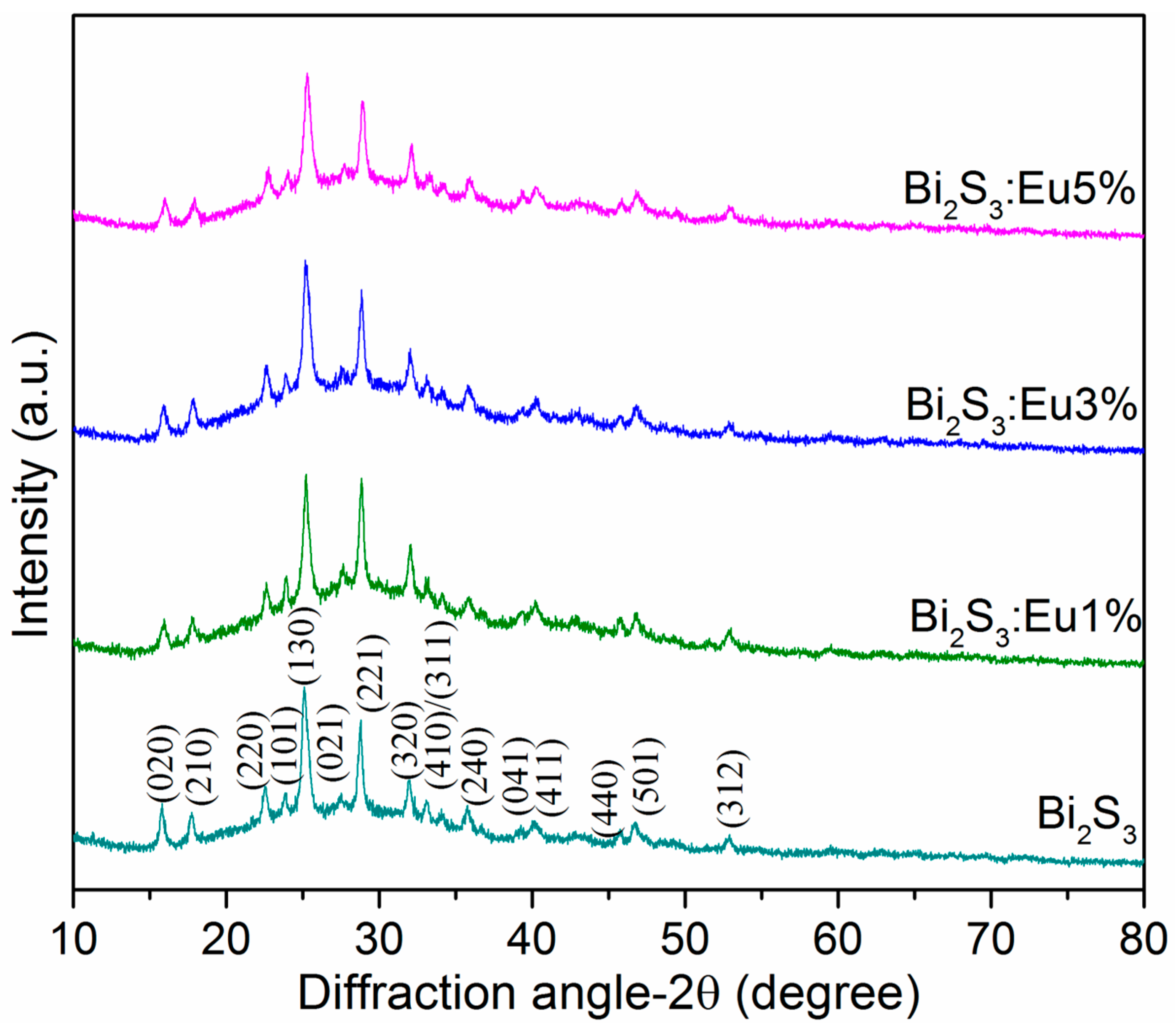
3.1. Structural Analysis

To explore the phase purity, as well as the crystalline constitution of the synthesized pure and Eu doped Bi2S3 films, and to determine whether the chosen dopant element in the current work effectively yielded high-quality films, XRD analysis was carried out at room temperature. Figure 1 allows for identification of the changes in Bi2S3 crystalline quality with respect to the diverse amount of Eu concentration. Two well-defined Bragg reflections belonging to the (130) and (221) planes and thirteen tiny Bragg reflections indexed to the (020), (210), (220), (101), (021), (320), (410), (240), (041), (411), (440), (501), and (312) planes were originated from the conventional orthorhombic formation of Bi2S3, and they have the same appearance as JCPDS No. 43-1471 [26]. According to the results, the (130) peak is the dominant peak for both the undoped and doped samples. The greater number of strong and narrow peaks show the polycrystalline and good crystallinity of the samples. From this observation, all the samples displayed similar diffraction peaks as to those exhibited by the undoped sample. However, the inserted Eu element amplified the strength of the peaks steadily up to 3%, and above 3%, it affects the quality of the peaks due to lattice distortion. Further, we noticed that the crystalline quality directly depends on the amount of dopant concentration, and the 3% Eu doped Bi2S3 thin film sample has the highest crystalline nature. This suggests that the Eu element can easily replace the bismuth atom, owing to its close ionic radii, amplifying its crystallinity. However, for higher concentrations (5% Eu), it can only occupy at interstitial sites of bismuth, resulting in the decrease in crystallinity. Since no Eu related peaks are seen in the XRD profile, this proves the successful replacement of the bismuth atom by the Eu element in the synthesized samples. It is noteworthy that high crystalline quality is one of the basic parameters which helps to increase the photosensing properties [27].
It is well known that a material’s current conduction property mainly depends upon mean crystallite size. The Debye–Scherrer empirical equation [28] was applied to the most influential diffraction peak (130) to compute the mean crystallite size and the existing microstrain of the nano-crystallites Bi2S3 thin films. The computed results are reported in Table 1.
D = 0.9   λ β   cos   θ
ε = β   cot   θ 4
where D is average crystalline size, and ε, λ, β, θ stand for micro strain, X-ray wavelength, full width of the dominant (130) peak, and the peak Bragg’s angle, respectively.
The computed crystallite size for pure and Bi2S3: Eu (1, 3, and 5%) thin films are 21, 24, 25, and 19 nm, respectively. As a consequence of Eu dopant, the crystallite size was found to be improved, and the sample made with a 3% Eu has the largest crystallite size of 25 nm, which is expected to display better photosensing results. The reason is that the large grain size can increase the absorption of the coated sample, which may help to increase light-current properties by generation of the electron–hole pair [29]. The other possible reason is that the larger grains reduce the grain boundaries, easing the electron transformation. The micro strain developed in the films is lessened from 7.46 × 10⁻³ to 6.28 × 10⁻³, and it was the smallest for 3% Eu doped Bi2S3 thin film. This implies that the dopant and parent materials stabilize the surfaces/grain boundaries and resist the formation of different types of deforming forces. This indicates the reduction of crystal misalignment or crystal imperfections. This verifies the formation of high quality superior films [30]. Recently, Devi et al. [22] observed a similar kind of crystallite size and strain variation for improved photosensing.
To study the doping fraction insertion, the lattice parameters (a, b, c) and cell volume of orthorhombic Bi2S3 thin films were estimated using the following equations, as presented in Table 1.
1 d 2 = ( h 2 a 2 + k 2 b 2 + l 2 c 2 )
V = a b c
The estimated values of the lattice parameter for pure Bi2S3 thin film is a = 11.254 Å, b = 3.9690 Å, and c = 11.099 Å, which fit well with those in previously reported works [13,31]. As a consequence of the Eu element, one can observe that the lattice parameter and cell volume values are expanded. This expansion, which developed in the Eu doped Bi2S3 thin films, can be due to the difference between the ionic radii (Eu3+ = 0.95 Å) (Bi3+= 0.103 nm) and the strains developed in the samples [32].

3.2. Morphology Studies

The FE-SEM photographs (Figure 2) were taken to assess the dopant impact (0, 1, 3, and 5%) on the surface structure and morphology of the Bi2S3 films; these are provided in Figure 2a–d. From the results, we noticed a continuous variation in the surface nature due to the dopant element. The parent Bi2S3 thin film consisted of closely packed rod-like uniform grains, which were grown nearly vertically to the glass substrates. Usually, this kind of rod-like grains facilitates charge separation due to the least diffusion distance [10]. Yue Wang et al. [33] recorded a rod-like nanostructure for spray-coated Bi2S3 thin films. When the dopant content increases to 3%, an uneven/irregular nanorod is noted, and the length as well as diameter of the nanorod is increased. On the other hand, in the case of Bi2S3: Eu (5%), the formation of a nanorod structure has almost vanished. It is worth noting that the density of nanorods per unit area is high for the Bi2S3:Eu (3%) sample. This property is vital, as it can reduce current leakage and promote the mode of electron flow, as well as photon absorption ability due to increased surface area [30,34]. Therefore, these results can allow the Bi2S3: Eu (3%) sample to yield better photodetection results.
Further, to understand the purity of the Bi2S3 samples, Energy Dispersive X-ray spectrum (EDX) images were obtained. Figure 3, showing the Bi2S3: Eu (3%) sample, specifies the presence of required elements such as Bi, S, and Eu. The attained spectrum proves the purity of the coated sample.

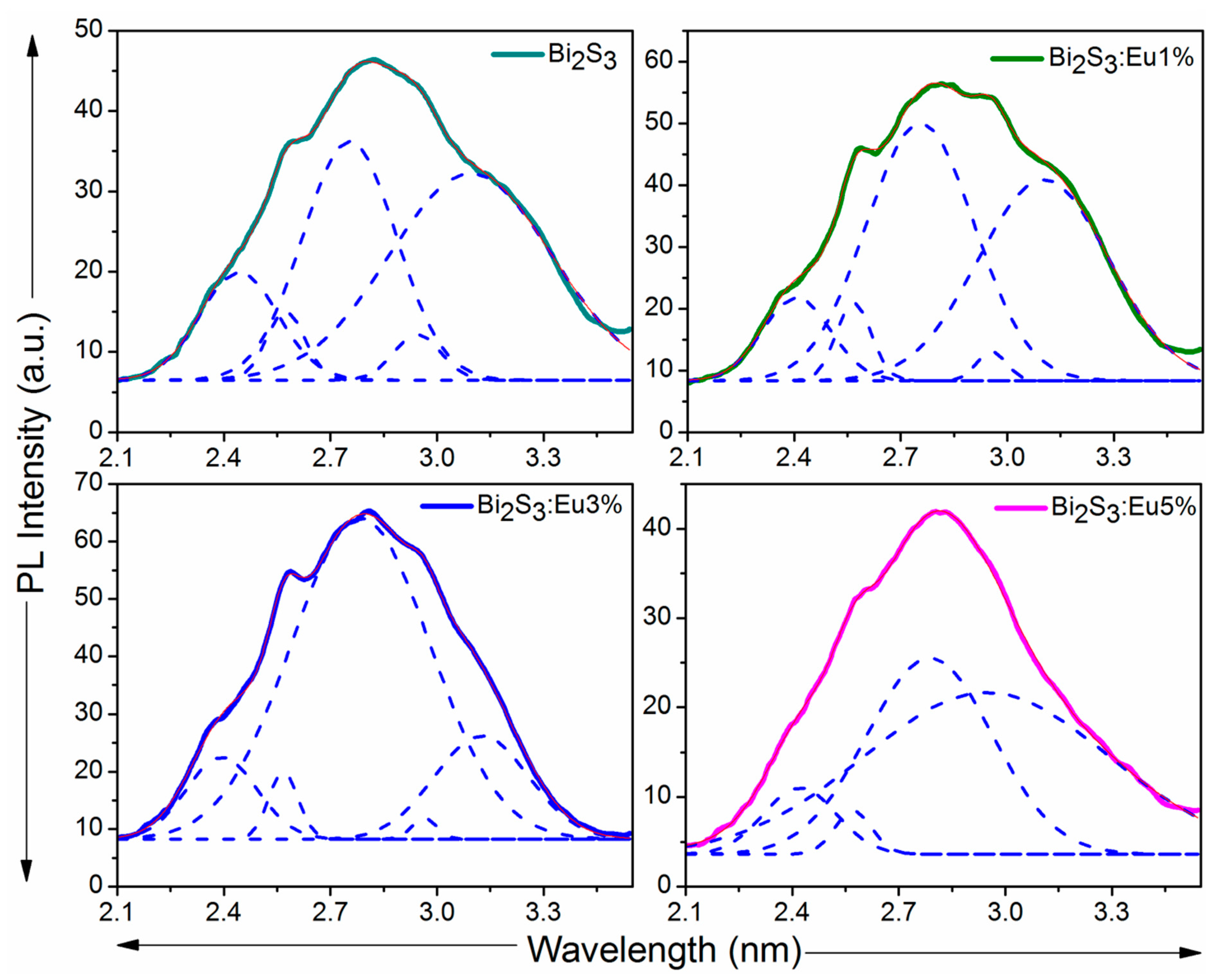
3.3. Photoluminescence (PL) Analyses

To further investigate the fate of the electron–hole pairs, photoresponsive sites, band gap energy, and defects present in the spray coated Eu doped Bi2S3 thin films, photoluminescence spectroscopic analysis is useful. The PL emission spectra (350–600 nm) of all the readied Bi2S3 samples are presented in Figure 4. As is seen in Figure 4, upon excitation at 325 nm (3.81 eV), the coated samples featured four distinct photoresponsive emission bands around 400 nm (3.1 eV), 427 nm (2.9 eV), 459 nm (2.7 eV), 482 nm (2.57 eV), and 516 nm (2.4 eV) nm. The first band appeared around 400 nm (3.1 eV), which might be because of the band-to-band emission, or band edge luminescence, that arises from the recombination of the excitons [35]. The second, third, and fourth peaks around 427 nm (2.9 eV) and 459 nm (2.7 eV), and existing in the violet region, are associated defects related to Bi and S [36]. The final green emission peak identified at 516 nm (2.4 eV) is a characteristic high-level transition of Bi2S3 nanocrystallites which appears due to trapped electron–hole pairs recombination [26]. Compared to the parent sample, the PL intensity is increased with increasing Eu3+ content, reaching high intensity for the 3% Eu doped Bi2S3 sample. Finally, the intensity drops for higher concentrations, i.e., the 5% Eu doped Bi2S3 sample. The high intensity indicates the higher recombination rate of the electron–hole pairs, increasing the surface area and crystallinity of the sample. This improvement in the crystallinity reduces the defects and raises the recombination of the excitons. It has been reported that these results can increase UV emissions [20]. On the other hand, the increased surface area of the sample subjected to the photon source will effectively improve the light absorption and charge carrier generation [37,38]. Further, it is seen that the addition of Eu content redshifts the peaks, which can cause the band gap of the sample to decrease.

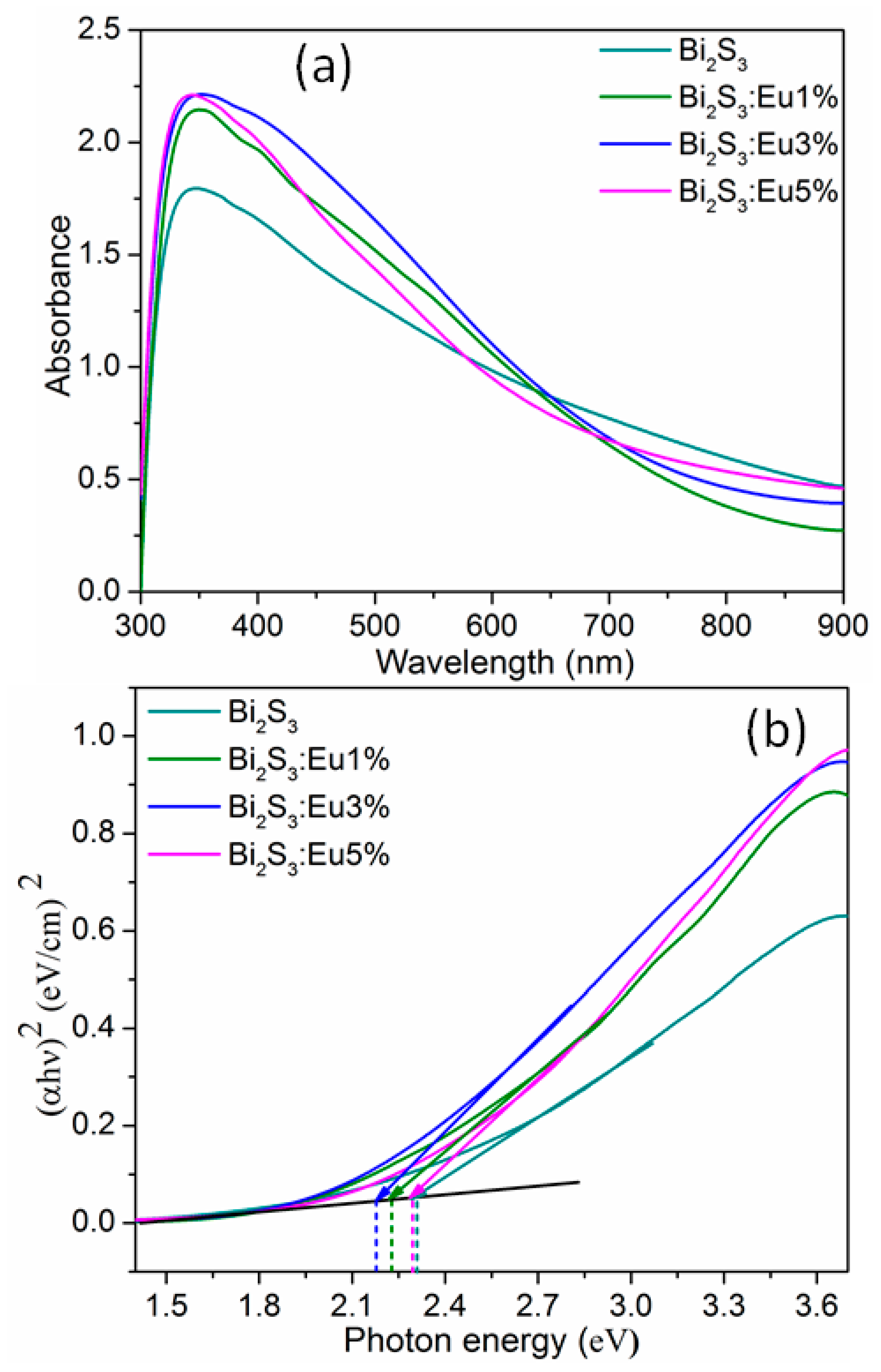
3.4. Optical Studies

The detailed photoabsorption and approximate energy band gap of the readied Bi2S3:Eu thin layers were documented between the wavelength range of 300–900 nm. The recorded UV/visible absorbance profiles are collectively given in Figure 5a. It is evident from Figure 5a that all the coated Bi2S3 thin layers displayed strong optical response in the UV regime, which is essential for UV photoresponse performance. As the dopant element enters into the parent material, the light absorption seemed to increase in the UV region, turning to drops after 400 nm. The Bi2S3: Eu (3%) featured the highest light absorption intensity over the other samples. This might be due to high grain size of the sample. The large grain size scatters the incident beam in all directions, and clearly enriches the light absorption ability [2,39]. The superlative light absorption ability can induce more charge carrier generation, which is considered as urgent for the photosensor. Thus, the coated Bi2S3: Eu (3%) can provide significant UV photosensing performance.
From the photoabsorption profile, the optical energy band gaps of both Bi2S3 and Eu doped Bi2S3 thin films were estimated using the well-known Tauc’s relation [26]
α h ν = A ( h ν E g ) 1 / 2
where Eg, denotes optical band gap and incident photon energy, and α, A represents absorption coefficient and proportionality constant respectively. The optical band gap is extracted from the plots hν vs. (αhν)2, which are shown in Figure 5b. In this work, the estimated band gaps of Bi2S3: Eu (0%), Bi2S3:Eu1%, Bi2S3:Eu3%, and Bi2S3:Eu5% are 2.29, 2.21, 2.17, and 2.28 eV. It is important to underline that the band gap is found to drop down, reaching its lowest level for Bi2S3: Eu3% thin film. The smallest band gap sample Bi2S3: Eu (3%) can easily complete the charge transfer process throughout the sample, which is beneficial for the photodetector. It is worth mentioning that the following factors, such as stoichiometry deviation, high photon-absorption level, orientation, and increased particle size of the sample, can reduce the band gap energy of the coated samples [2,40]. In the present case, the decrease in band gap is due to increased particle size and the generation of defects and disorder in the Bi2S3 lattice, which allow for the formation of localized states and deep levels in the band gap.

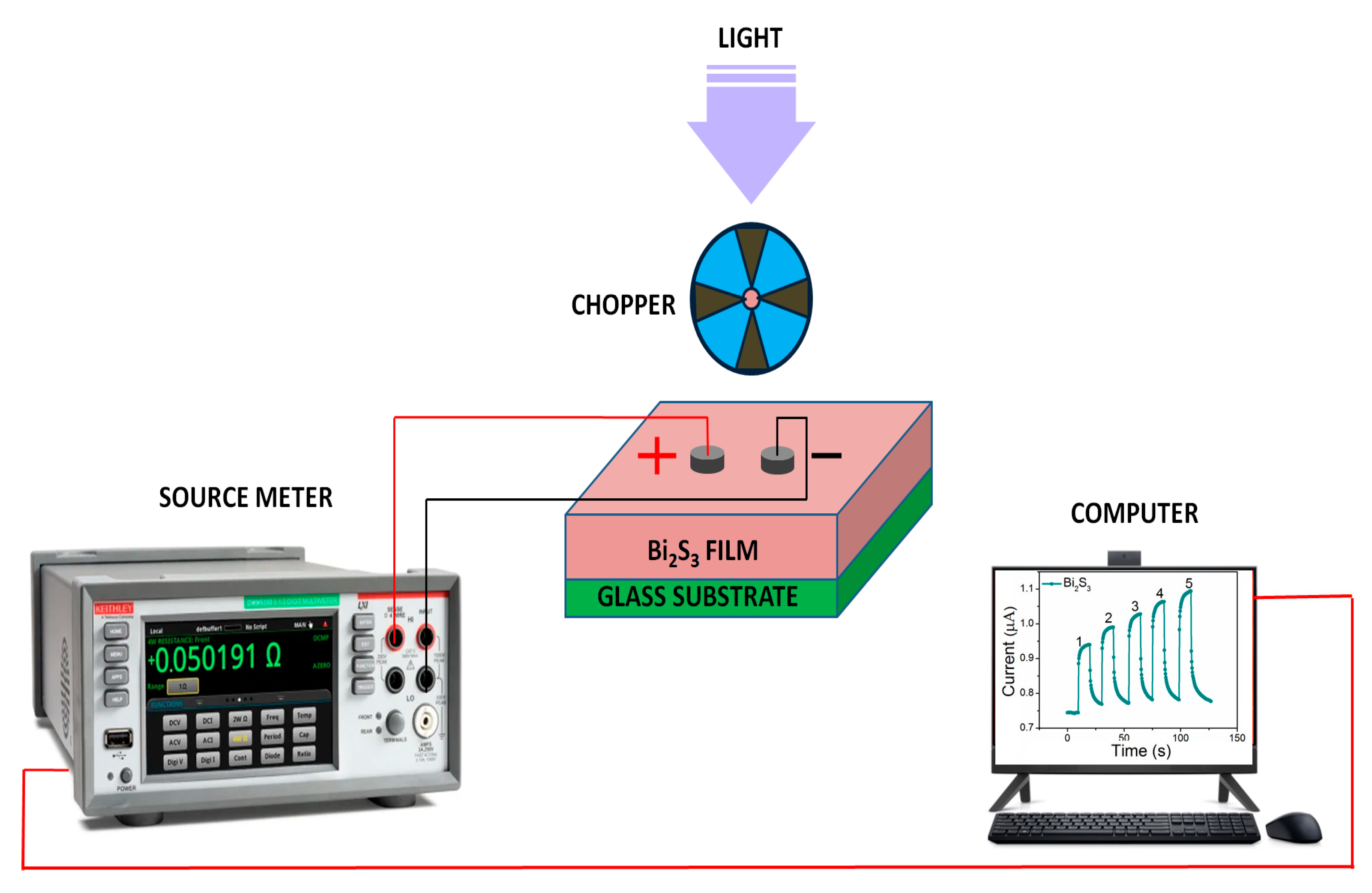
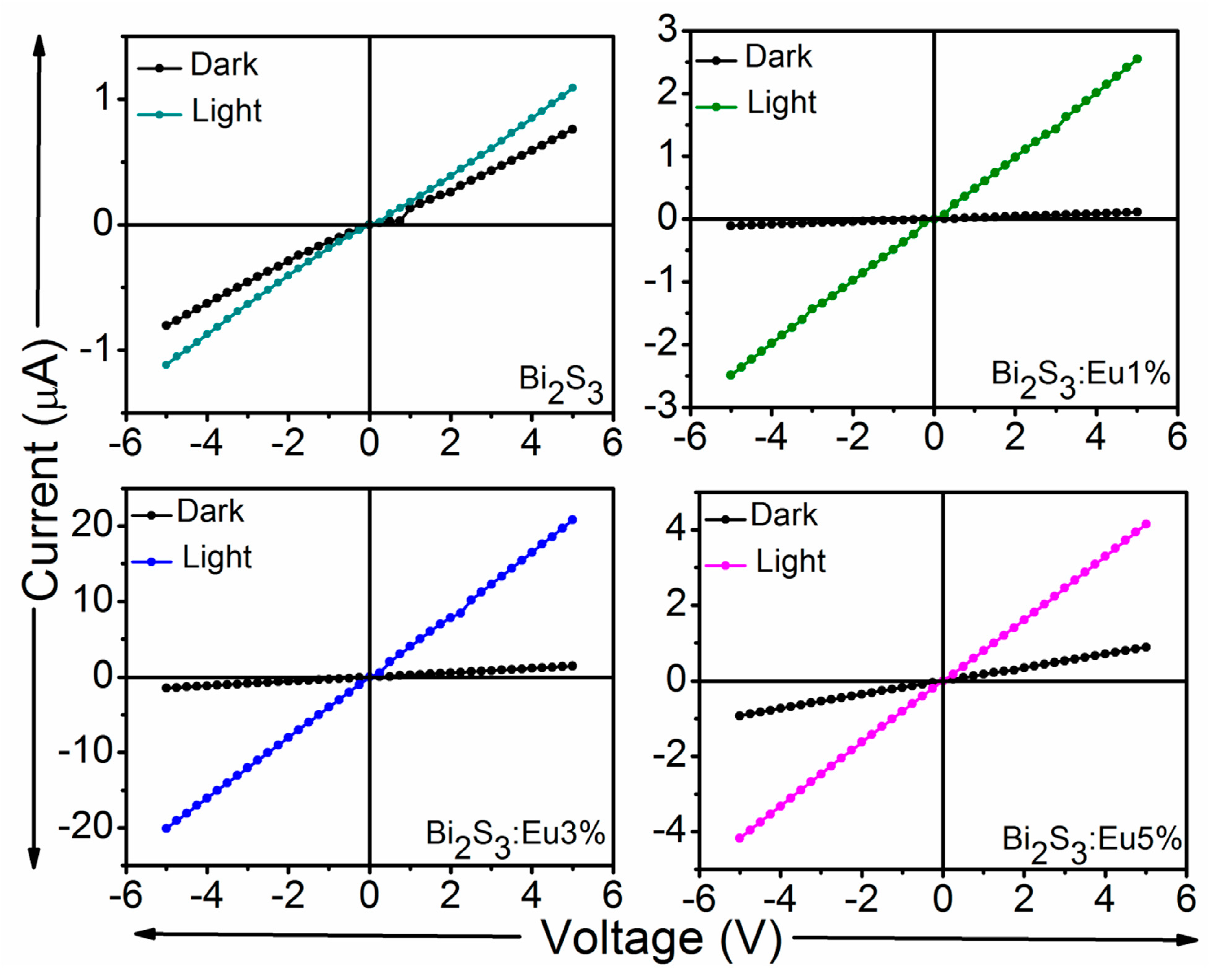
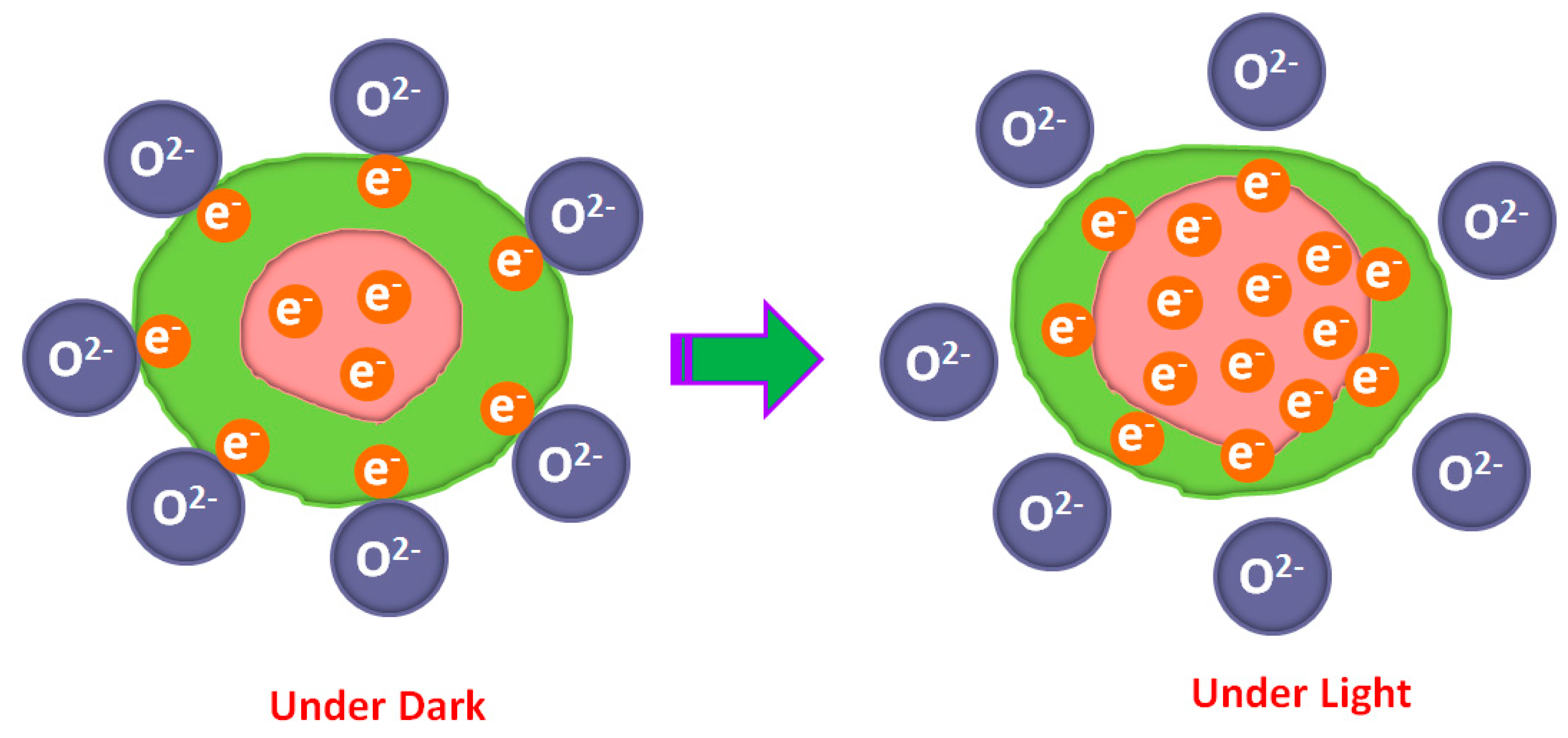
3.5. Photocurrent Studies

Finally, the light current properties (dark current (Id) and photocurrent (Iph)) of the present Bi2S3 nanorods for different weight percentages, recorded at room temperature in the presence of dark and light modes (365 nm) by applying constant bias voltage, ranges from −5 to +5 V. To make a photosensor, the deposited samples were taken in an area of 1 cm × 1 cm and silver paste was applied over the film to create working electrodes. The schematic depiction of the fabricated UV photosensor based on the Bi2S3 thin films is given in Figure 6. The plotted current variations, as a function of bias voltage (current-voltage (I−V)) characteristic of the present samples, are showed in Figure 7. Before measuring the dark current, the coated samples were kept in a dark state for about 10 h. The obtained dark current and photocurrent exhibit good linear trend characteristics as the applied voltage increases, suggesting the excellent formation of an ohmic junction between the Ag electrode and Bi2S3:Eu thin films. Under the light mode, a higher current is realized for all the samples, which proves the current ability of the present coated samples. The dark current of the Bi2S3: Eu (0%), Bi2S3: Eu (1%), Bi2S3: Eu (3%) and Bi2S3: Eu (5%) is 0.7 × 10⁻⁶, 0.4 × 10⁻⁶, 0.3 × 10⁻⁶, and 1 × 10⁻⁶ A, respectively. The observed dark current is very small, which is a necessary condition for an efficient photosensor. This dark current will improve the detection performance. With the increase in the Eu doping concentration, the light current gradually increases from 1.2 × 10⁻⁶ A to 21 × 10−6 A, attaining a maximum value of 21 × 10−6 A for Bi2S3:Eu the 3% sample under the same illumination conditions. These interesting responses of the Bi2S3:Eu3% sample are mostly related to the good structure and film quality, low defect density, increased separation of electron–hole pairs, less recombination of charge couples, good ohmic contact of the Ag and Bi2S3 thin film, reduced band gap (which allows for the absorption of more photons), and increased crystallite size, which reduces the grain boundary, causing improvement in the electrical conductivity [25,40,41].
Apart from the cost of the photosensor, understanding the three most essential parameters, i.e., photoresponsivity (R), detectivity (D*), and external quantum efficiency (EQE) of the light detector is vital, and they were calculated using the given equations (Equations (6)–(8)). The calculated R, D*, and EQE values of the presented Bi2S3: Eu samples are given in Figure 8.
R = I p P i n   ×   A
D * = R A 2 ε I d
EQE = R h c e λ
The parameters A, Ip, Pin stand for the active sensitive area of the sample, the photocurrent, and power of the light source, while the symbols λ, e, Id, h, and c, denote the wavelength of incident light, electron charge value, dark current, Planck’s constant, and velocity of light, respectively. The plotted graph (Figure 8) reveals that the Bi2S3: Eu (3%) sample displayed better R (3.88 × 10⁻¹ AW−1), D* (1.82 × 10¹⁰ Jones), and EQE (125%) values than the other coated samples.
We conducted further research on the time-dependent key factors, i.e., the detection speed (response time and recovery time) of the present photodetector with respect to the ON/OFF light source at 5 bias voltage. The temporal photoresponse plots of the presented Bi2S3: Eu samples are shown in Figure 9. When the UV light was turned on, the photocurrent response of the samples shows dramatic enhancement, with rapid saturation. A sharp fall to the initial dark current value is noted when the light is switched off. This indicates the steady switching behavior of the prepared samples. The recorded rise/fall speed of the Bi2S3: Eu (0%), Bi2S3: Eu (1%), Bi2S3: Eu (3%), and Bi2S3: Eu (5%) thin films were found to be in the order of 2.6/2.8 s,1.3/1.4 s, 0.3/0.4 s, and 0.4/0.4 s, respectively. The recovery time of all the samples is observed to be slightly lower than the response speed, and the Bi2S3: Eu (3%) thin film displayed the lowest value of rise/decay time compared to the other deposited samples, which proves the high detection speed of the sample. The fast rise and fall times of Bi2S3: Eu (3%) thin film is owing to the rapid electron−hole pair generation and recombination rate. Generally, the nanorods have a high surface-to-volume ratio and will act as recombination centers for the charge carriers, leading to a rapid rise/fall time [4].
In this section, we compare the performance of the previously reported literature with the currently developed photosensor for a better and more clear understanding of the current study; the compared performance parameters are listed in Table 2. Veeralingam et al. [42] manufactured Bi2S3 microneedles/RuS2 nanorods, and the heterostructure formation shows the maximum responsivity of 39 × 10−3 A/W. Paulraj et al. [43] observed a high responsivity value of 0.29 AW−1 for an Sm doped Zns photosensor developed via the nebulizer spray technique. Shaikh et al. [44] annealed a CdS–Bi2S3 heterojunction photodetector which exhibited notable photosensitivity of 0.43 A/W. The Bi2S3/rGO heterojunction based photosensor synthesized by Ladan et al. [45] displayed a rapid response/recovery speed of 175/401 s. Recently, Jesu et al. [46] fabricated nebulizer sprayed Cu doped ZnS thin films that showed notable R (2.24 × 10⁻² AW−1), D* (2.66 × 10¹⁰ Jones), and EQE (7.23%) values. Rajeswari et al. [26] also coated Fe doped Bi2S3 samples, displaying reasonable parameter values of R = 9.60 × 10⁻² AW−1, D* = 1.34 × 10¹⁰ Jones, and EQE = 22.4%, with a rapid rise/fall speed of 0.3/0.4 s. The photosensing data of the present Eu doped Bi2S3 sample is higher than these previously reported values.
The three possible phenomena behind the photoresponse mechanism of the manufactured Bi2S3 photodetector are photon absorption, photocurrent generation, and transportation of the photocarriers. On the other hand, the photoresponse is mainly achieved by the adsorption and desorption of oxygen molecules, which modify the photocurrent production. Under dark conditions, the adsorption of oxygen molecules on the top surface of the samples received the negatively charged ion (O2 + e = O2). This process widens the depletion layer. When UV light falls on the surface of the Bi2S3 sample, its energy is absorbed, and electron–hole pairs are produced. The holes produced during light absorption discharge the negatively charged ion (h+ + O2 → O2). This effect makes the depletion layer very thin, causing the charge carriers to easily penetrate the layer, causing an increase in the photocurrent. This process is described in Figure 10.

4. Conclusions

In summary, for the first time, we have prepared a low-cost, easy, nontoxic, and highly UV sensitive pure Bi2S3, as well as an Eu 1–5 wt.%-doped Bi2S3 thin film on a cleaned glass substrate. The incorporation of Eu provides the larger 25 nm grains for the Bi2S3: Eu (3%) thin film. The formation of a nanorod structure is confirmed by FESEM photos. High absorption and a low optical band gap (2.17 eV) were noticed for the 3% Eu doped sample. The conducted I-V test showed that the coated thin films exhibited admirable photocurrent conversion for the UV source. The Bi2S3 film with 3% Eu concentration displayed high performance with photoresponsivity, detectivity, and external quantum efficiency of 3.88 × 10⁻¹ AW−1, 1.82 × 10¹⁰ Jones, 125% at 5 V, respectively. The findings of the current study can be used in advanced functional optoelectronic applications.

Author Contributions

Conceptualization, M.S.; Funding acquisition, A.B.G.T. and F.H.A.; Investigation, S.A.; Methodology, M.S., A.B.G.T. and F.H.A.; Project administration, F.H.A.; Supervision, F.H.A.; Writing—original draft, M.S. and F.H.A.; Writing—review & editing, M.S., A.B.G.T., F.H.A., S.A., B.P. and M.U. All authors have read and agreed to the published version of the manuscript.

Funding

This research was funded by Princess Nourah bint Abdulrahman University Researchers Supporting Project number (PNURSP2022R38), Princess Nourah bint Abdulrahman University, Riyadh, Saudi Arabia. The authors extend their appreciation to the Deanship of Scientific Research at King Khalid University for funding this work through a Research Groups Program under Grant No. R.G.P. 2/249/43.

Data Availability Statement

The raw/processed data required to reproduce these findings cannot be shared at this time as the data also forms part of an ongoing study.

Acknowledgments

This research was funded by Princess Nourah bint Abdulrahman University Researchers Supporting Project number (PNURSP2022R38), Princess Nourah bint Abdulrahman University, Riyadh, Saudi Arabia. The authors extend their appreciation to the Deanship of Scientific Research at King Khalid University for funding this work through a Research Groups Program under Grant No. R.G.P. 2/249/43.

Conflicts of Interest

The authors declare no conflict of interest.

References

  1. Salsabilla, A.; Fauzia, V.; Imawan, C. The effect of addition of WS2 nanosheets on the performance of ZnO nanorods-based photodetector. J. Phys. Conf. Ser. 2022, 2274, 012002. [Google Scholar] [CrossRef]
  2. Hakam, J. Highly induced photosensing behavior of Erbium (Er), Yttrium (Y) and Terbium (Tb) doped nanostructured Cadmium Sulphide (CdS) thin films prepared by nebulizer spray pyrolysis method. J. Alloys Comp. 2022, 924, 166577. [Google Scholar] [CrossRef]
  3. JabirHakami, P.N.; Manikandan, M.; Singh, V.; Palani, I. Investigations on LSPR effect of Cu/Al nanostructures on ZnO nanorods towards photodetector applications. J. Lumin. 2021, 238, 118331. [Google Scholar] [CrossRef]
  4. Saeed, S.; Dai, R.; Janjua, R.A.; Huang, D.; Wang, H.; Wang, Z.; Ding, Z.; Zhang, Z. Fast-Response Metal−Semiconductor−Metal Junction Ultraviolet Photodetector Based on ZnS:Mn Nanorod Networks via a Cost-Effective Method. ACS Omega 2021, 6, 32930–32937. [Google Scholar] [CrossRef]
  5. Arumugam, J.; George, A.; Raj, A.D.; Irudayaraj, A.A.; Josephine, R.; Sundaram, S.J.; Algarni, T.S.; Al-Mohaimeed, A.M.; Balasubramanian, B.; Kaviyarasu, K. Improved Ag doped Bi2S3 nanowire-based photodiode: Fabrication and performance. Mater. Lett. 2021, 302, 130403. [Google Scholar] [CrossRef]
  6. Motaung, M.P.; Onwudiwe, D.C.; Lei, W. Microwave-Assisted Synthesis of Bi2S3 and Sb2S3 Nanoparticles and Their Photoelectrochemical Properties. ACS Omega 2021, 6, 18975–18987. [Google Scholar] [CrossRef] [PubMed]
  7. Fazal, T.; Ismail, B.; Wafee, S.; Kambooh, A.H.; Khan, A.R. Cu doped Bi2S3 as potential absorbers for thin film solar cells: Optical and structural properties. Chalcogenide Lett. 2016, 13, 225–231. [Google Scholar]
  8. Mahuli, N.; Saha, D.; Sarkar, S.K. Atomic Layer Deposition of p-Type Bi2S3. J. Phys. Chem. C 2017, 121, 8136–8144. [Google Scholar] [CrossRef]
  9. Ajiboye, T.O.; Onwudiwe, D.C. Bismuth sulfide based compounds: Properties, synthesis and applications. Results Chem. 2021, 3, 100151. [Google Scholar] [CrossRef]
  10. Geng, Y.-Y.; Tao, C.-L.; Duan, S.-F.; Martin, J.S.; Lin, Y.; Zhu, X.; Zhang, Q.-Q.; Kang, X.-W.; He, S.-S.; Zhao, Y.-X.; et al. V-rich Bi2S3 nanowire with efficient charge separation and transport for high-performance and robust photoelectrochemical application under visible light. Catal. Today 2020, 350, 47–55. [Google Scholar] [CrossRef]
  11. Lokhande, R.; Thakur, S.; Chate, P. Bi2S3 thin films: Optical and crystallography studies. Optik 2020, 219, 165230. [Google Scholar] [CrossRef]
  12. Xiao, G.; Dong, Q.; Wang, Y.; Sui, Y.; Ning, J.; Liu, Z.; Tian, W.; Liu, B.; Zou, G. One-step solution synthesis of bismuth sulfide (Bi2S3) with various hierarchical architectures and their photoresponse properties. RSC Adv. 2012, 2, 234–240. [Google Scholar] [CrossRef]
  13. Desale, D.J.; Shaikh, S.; Siddiqui, F.; Birajdar, R.; Late, R.; Ghule, A.; Sharma, R. Enhancement of photosensitivity by annealing in Bi2S3 thin films grown using SILAR method. Compos. Part B Eng. 2013, 46, 1–6. [Google Scholar] [CrossRef]
  14. Shaikh, S.U.; Siddiqui, F.Y.; Singh, F.; Kulriya, P.K.; Phase, D.; Sharma, R. Modification of photosensing property of CdSe-Bi2S3 bi-layer by thermal annealing and swift heavy ion irradiation. Mater. Chem. Phys. 2015, 169, 6–12. [Google Scholar] [CrossRef]
  15. Zhou, W.; Li, Y.; Huang, H.; Wang, J.; Zhong, F. Preparation and photoelectric properties of holmium-doped bismuth sulfide film. Mater. Sci. Semicond. Processing 2022, 143, 106467. [Google Scholar] [CrossRef]
  16. Hajimazdarani, M.; Ghasali, E.; Naderi, N.; Orooji, Y. Enhanced optical properties and photodetection behavior of ZnS thin film deposited by electron beam evaporation upon doping with europium oxide. Ceram. Int. 2020, 46, 28382–28389. [Google Scholar] [CrossRef]
  17. Sarkar, A.; Ghosh, A.B.; Saha, N.; Dutta, A.K.; Srivastava, D.N.; Paul, P.; Adhikary, B. Enhanced photocatalytic activity of Eu doped Bi2S3 nanoflowers for degradation of organic pollutants under visible light illumination. Catal. Sci. Technol. 2015, 5, 4055–4063. [Google Scholar] [CrossRef]
  18. Shkir, M.; Ashraf, I.; Chandekar, K.V.; Yahia, I.; Khan, A.; Algarni, H.; AlFaify, S. A significant enhancement in visible-light photodetection properties of chemical spray pyrolysis fabricated CdS thin films by novel Eu doping concentrations. Sens. Actuators A Phys. 2020, 301, 111749. [Google Scholar] [CrossRef]
  19. Shwetha, M.; Eraiah, B. Thermal properties, FTIR characteristics and Physical parameters of Europium Oxide doped Phosphate Glasses. AIP Conf. Proc. 2020, 2220, 080045. [Google Scholar] [CrossRef]
  20. Hasabeldaim, E.; Ntwaeaborwa, O.; Kroon, R.; Swart, H. Structural, optical and photoluminescence properties of Eu doped ZnO thin films prepared by spin coating. J. Mol. Struct. 2019, 1192, 105–114. [Google Scholar] [CrossRef]
  21. Arulanantham, A.M.S.; Raj, P.M.; Gunavathy, K.V.; Begam, M.R.; Ganesh, V.; Algarni, H. Photosensitivity properties of Eu-doped SnS2 thin films deposited by cost-effective nebulizer spray pyrolysis technique. Appl. Phys. A 2022, 128, 364. [Google Scholar] [CrossRef]
  22. Devi, M.D.; Juliet, A.V.; Ade, R.; Thirumoorthi, M.; Diana, P.; Saravanakumar, S.; Ganesh, V.; Bitla, Y.; Algarni, H. Enhancement in optoelectronic properties of europium-doped ZnS thin films prepared by nebulizer spray technique for UV photodetection applications. Mater. Sci. Semicond. Processing 2022, 144, 106572. [Google Scholar] [CrossRef]
  23. Tarachand; Sharma, V.; Bhatt, R.; Ganesan, V.; Okram, G.S. A catalyst-free new polyol method synthesized hot-pressed Cu-doped Bi2S3 nanorods and their thermoelectric properties. Nano Res. 2016, 9, 3291–3304. [Google Scholar] [CrossRef]
  24. Yu, X.; Cao, C. Photoresponse and Field-Emission Properties of Bismuth Sulfide Nanoflowers. Cryst. Growth Des. 2008, 8, 3951–3955. [Google Scholar] [CrossRef]
  25. Albargi, H.; Khan, Z.; Marnadu, R.; Ammar, H.; Algadi, H.; Umar, A.; Ashraf, I.; Shkir, M. Fabrication and characterization of high-performance photodetectors based on Au/CdS/Au and Au/Ni:CdS/Au junctions. J. King Saud Univ.-Sci. 2021, 33, 101638. [Google Scholar] [CrossRef]
  26. Rajeswari, S.; Ibrahim, M.M.; Raj, I.L.P.; Hakami, J.; Imran, M.; AlFaify, S.; Shkir, M. Noticeably enhanced photosensing properties of Fe-doped Bi2S3 thin films developed by nebulizer spray pyrolysis technique for photosensor applications. Sens. Actuators A Phys. 2022, 345, 113759. [Google Scholar] [CrossRef]
  27. Shkir, M. Enhancement in optical and electrical properties of ZnO thin films via Co doping for photodetector applications. Mater. Sci. Eng. B 2022, 284, 115861. [Google Scholar] [CrossRef]
  28. Raj, I.L.P.; Valanarasu, S.; Isaac, R.R.; Ramudu, M.; Bitla, Y.; Ganesh, V.; Yahia, I. The role of silver doping in tuning the optical absorption, energy gap, photoluminescence properties of NiO thin films for UV photosensor applications. Opt.-Int. J. Light Electron Opt. 2022, 254, 168634. [Google Scholar] [CrossRef]
  29. Raj, I.L.P.; Valanarasu, S.; Abdeltawab, A.A.; Mohammady, S.Z.; Ubaidullah, M.; Shaikh, S.F.; Shkir, M. Improved UV photosensing properties of high crystalline nickel oxide thin films: Role of yttrium doping. Opt.-Int. J. Light Electron Opt. 2021, 248, 168105. [Google Scholar] [CrossRef]
  30. Mohan, K.; Panneerselvam, A.; Marnadu, R.; Chandrasekaran, J.; Shkir, M.; Tataroğlu, A. A systematic influence of Cu doping on structural and opto-electrical properties of fabricated Yb2O3 thin films for Al/Cu-Yb2O3/p-Si Schottky diode applications. Inorg. Chem. Commun. 2021, 129, 108646. [Google Scholar] [CrossRef]
  31. Madoun, M.; Baghdad, R.; Chebbah, K.; Bezzerrouk, M.; Michez, L.; Benramdane, N. Temperature effect on structural and optoelectronic properties of Bi2S3 nanocrystalline thin films deposited by spray pyrolysis method. Mater. Sci. Semicond. Process. 2013, 16, 2084–2090. [Google Scholar] [CrossRef]
  32. Shaili, H.; Salmani, E.; Beraich, M.; Zidane, M.; Taibi, M.; Rouchdi, M.; Ez-Zahraouy, H.; Hassanain, N.; Mzerd, A. Higher Conductivity and Enhanced Optoelectronic Properties of Chemically Grown Nd-Doped CaSnO3 Perovskite Oxide Thin Film. ACS Omega 2021, 6, 32537–32547. [Google Scholar] [CrossRef] [PubMed]
  33. Wang, S.-Y.; Du, Y.-W. Preparation of nanocrystalline bismuth sulfide thin films by asynchronous-pulse ultrasonic spray pyrolysis technique. J. Cryst. Growth 2002, 236, 627–634. [Google Scholar] [CrossRef]
  34. Muhammad, A.; Hassan, Z.; Mohammad, S.M.; Rajamanickam, S.; Shitu, I.G. Fabrication of ultra-violet photodetector with enhanced optoelectronic parameters using low-cost F-doped ZnO nanostructures. Sens. Actuators A Phys. 2021, 332, 113092. [Google Scholar] [CrossRef]
  35. Salavati-Niasari, M.; Behfard, Z.; Amiri, O.; Khosravifard, E.; Mashkani, S.M.H. Hydrothermal Synthesis of Bismuth Sulfide (Bi2S3) Nanorods: Bismuth(III) Monosalicylate Precursor in the Presence of Thioglycolic Acid. J. Clust. Sci. 2013, 24, 349–363. [Google Scholar] [CrossRef]
  36. Fazal, T.; Iqbal, S.; Shah, M.; Bahadur, A.; Ismail, B.; Abd-Rabboh, H.S.M.; Hameed, R.; Mahmood, Q.; Ibrar, A.; Nasar, M.S.; et al. Deposition of bismuth sulfide and aluminum doped bismuth sulfide thin films for photovoltaic applications. J. Mater. Sci. Mater. Electron. 2022, 33, 42–53. [Google Scholar] [CrossRef]
  37. Raj, I.L.P.; Valanarasu, S.; Prasad, K.H.; Ponraj, J.S.; Chidhambaram, N.; Ganesh, V.; Ali, H.E.; Khairy, Y. Enhancement of optoelectronic parameters of Nd-doped ZnO nanowires for photodetector applications. Opt. Mater. 2020, 109, 110396. [Google Scholar] [CrossRef]
  38. Anastasescu, C.; Zaharescu, M.; Angelescu, D.; Munteanu, C.; Bratan, V.; Spataru, T.; Negrila, C.; Spataru, N.; Balint, I. Defect-related light absorption, photoluminiscence and photocatalytic activity of SiO2 with tubular morphology. Sol. Energy Mater. Sol. Cells 2017, 159, 325–335. [Google Scholar] [CrossRef]
  39. Lavanya, S.; Kumar, T.R.; Gunavathy, K.V.; Vibha, K.; Shkir, M.; Hakami, J.; Ali, H.E.; Ubaidullah, M. A noticeable improvement in opto-electronic properties of nebulizer sprayed In2S3 thin films for stable-photodetector applications. Micro Nanostructures 2022, 169, 207337. [Google Scholar] [CrossRef]
  40. Rajeswari, S.; Ibrahim, M.M.; Al-Enizi, A.M.; Ubaidullah, M.; Arunachalam, P.; Pandit, B.; Shaikh, S.F. Photo-sensing properties of Cd-doped In2S3 thin films fabricated via low-cost nebulizer spray pyrolysis technique. J. Mater. Sci. Mater. Electron. 2022, 33, 19284–19296. [Google Scholar] [CrossRef]
  41. Khan, Z.; Revathy, M.; Shkir, M.; Khan, A.; Sayed, M.; Umar, A.; Alshammari, A.S.; Vinoth, S.; Marnadu, R.; Yousef, E.S.; et al. Noticeably enhanced opto-electrical and photodetection performance of spray pyrolysis grown Mn:CdS nanostructured thin films for visible-light sensor applications. Surf. Interfaces 2022, 28, 101586. [Google Scholar] [CrossRef]
  42. Veeralingam, S.; Badhulika, S. Bi-Metallic sulphides 1D Bi2S3 microneedles/1D RuS2 nano-rods based n- n heterojunction for large area, flexible and high-performance broadband photodetector. J. Alloy. Compd. 2021, 885, 160954. [Google Scholar] [CrossRef]
  43. Paulraj, K.; Ramaswamy, S.; Chidhambaram, N.; Algarni, H.; Shkir, M.; AlFaify, S. Investigation of samarium-doped PbS thin films fabricated using nebulizer spray technique for photosensing applications. Superlattices Microstruct. 2020, 148, 106723. [Google Scholar] [CrossRef]
  44. Shaikh, S.U.; Siddiqui, F.Y.; Desale, D.J.; Ghule, A.V.; Singh, F.; Kulriya, P.K.; Sharma, R. Effect of swift heavy ion irradiation on structural and opto-electrical propertiesofbi-layerCdS–Bi2S3 thin films prepared by solution growth technique at room temperature. Radiat. Phys. Chem. 2015, 106, 193–198. [Google Scholar] [CrossRef]
  45. Heshmatynezhad, L.; Jamali-Sheini, F.; Monshi, A. Transient photocurrent response of Bi2S3/rGO nanocomposites synthesized by UV-assisted sonication method. Mater. Res. Express 2019, 6, 086332. [Google Scholar] [CrossRef]
  46. Jebathew, A.J.; Karunakaran, M.; Ade, R.; Ponraj, J.S.; Ganesh, V.; Manavalan, R.K.; Bitla, Y.; Yahia, I.S.; Algarni, H. Highly sensitive hexagonal-shaped ZnS–Cu thin films for photo-detector applications. J. Mater. Sci. Mater. Electron. 2022, 33, 2192–2203. [Google Scholar] [CrossRef]
Figure 1. XRD pattern of un-doped and Eu doped Bi2S3 thin films.
Crystals 12 01329 g001
Figure 2. FESEM images of Eu-doped Bi2S3 thin films with different Eu concentrations (a) 0%, (b) 1%, (c) 3%, and (d) 5%.
Crystals 12 01329 g002
Figure 3. EDX spectrum of 3% Eu-doped Bi2S3 thin film.
Crystals 12 01329 g003
Figure 4. Photoluminescence spectra of Eu-doped Bi2S3 thin films with different Eu concentrations.
Crystals 12 01329 g004
Figure 5. (a) Absorption spectra and (b) Tauc plots of Eu-doped Bi2S3 thin films with different Eu concentrations.
Crystals 12 01329 g005
Figure 6. The schematic depiction of the fabricated UV photosensor.
Crystals 12 01329 g006
Figure 7. Semi-log I–V characteristics of the fabricated Eu-doped Bi2S3 photosensor measured under dark and illuminated conditions at a bias voltage between −5 and +5 V, prepared using different Eu doping concentrations.
Crystals 12 01329 g007
Figure 8. Responsivity, detectivity, and external quantum efficiency of the Eu-doped Bi2S3 photosensor, with Eu doping concentrations.
Crystals 12 01329 g008
Figure 9. Plots of current vs. time of Eu-doped Bi2S3 photosensor using different Eu doping concentrations.
Crystals 12 01329 g009
Figure 10. Mechanism of the photoconductivity of the Bi2S3 thin film.
Crystals 12 01329 g010
Table 1. Crystallite size, strain, lattice constants, and cell volume of the Eu doped Bi2S3 thin films.
SamplesCrystallite Size (nm)Strain
×10−3
Lattice ConstantCell Volume (Å3)
a (Å)b (Å)c (Å)
Bi2S3217.4611.2543.969011.099496.0
Bi2S3:Eu1%246.7311.2583.97411.120497.6
Bi2S3: Eu3%256.2811.2653.97511.115497.7
Bi2S3: Eu5%198.2911.2773.97611.133499.2
Table 2. Comparison of the photosensor parameters of the current work with the previous sulfide-related photodetectors.
SampleResponsivity (AW−1)External Quantum Efficiency (EQE) (%)Detectivity (Jones)Rise Time (s)Fall Time (s)Ref.
Bi2S339 × 10−3--0.6-[42]
PbS:Sm0.29----[43]
CdS/ Bi2S30.43----[44]
Bi2S3/rGO---175401[45]
ZnS:Cu2.24 × 10−27.232.66 × 101013[46]
Bi2S3:Fe9.60 × 10−222.41.34 × 10100.30.4[26]
Bi2S3:Eu3.88 × 10−11251.82 × 10100.30.4Present work
Publisher’s Note: MDPI stays neutral with regard to jurisdictional claims in published maps and institutional affiliations.

