Article

Tunable Band Alignment in the Arsenene/WS2 Heterostructure by Applying Electric Field and Strain

1
School of Electrical and Mechanical Engineering, Pingdingshan University, Pingdingshan 467000, China
2
School of Physics, Henan Normal University, Xinxiang 453007, China
3
School of Mathematics and Physics, Henan University of Urban Construction, Pingdingshan 467036, China
*
Author to whom correspondence should be addressed.
Crystals 2022, 12(10), 1390; https://doi.org/10.3390/cryst12101390
Submission received: 28 August 2022 / Revised: 24 September 2022 / Accepted: 27 September 2022 / Published: 30 September 2022
(This article belongs to the Special Issue Novel Semiconductor Materials for Optoelectronic Applications)

Abstract

:
Arsenene has received considerable attention because of its unique optoelectronic and nanoelectronic properties. Nevertheless, the research on van der Waals (vdW) heterojunctions based on arsenene has just begun, which hinders the application of arsenene in the optoelectronic and nanoelectronic fields. Here, we systemically predict the stability and electronic structures of the arsenene/WS2 vdW heterojunction based on first-principles calculations, considering the stacking pattern, electric field, and strain effects. We found that the arsenene/WS2 heterostructure possesses a type-II band alignment. Moreover, the electric field can effectively tune both the band gap and the band alignment type. Additionally, the band gap could be tuned effectively by strain, while the band alignment type is robust under strain. Our study opens up a new avenue for the application of ultrathin arsenene-based vdW heterostructures in future nano- and optoelectronics applications. Our study demonstrates that the arsenene/WS2 heterostructure offers a candidate material for optoelectronic and nanoelectronic devices.

1. Introduction

Atomically thin two-dimensional (2D) materials have received continuous attention due to their novel physical and chemical properties [1,2,3,4,5]. Furthermore, a large number of 2D materials, such as phosphorene and stanine, have been successfully applied to field-effect transistors and photodetectors [6,7,8,9]. Recently, as with the analogs of 2D phosphorene, arsenene has gained a surge in research interest [10,11,12,13,14]. Arsenene possesses a rhombohedral monolayer structure, which is isolated from gray arsenic. High carrier mobility and excellent visible light absorption capacity make arsenene a candidate for photovoltaic and photocatalytic materials [15,16,17]. Studies have demonstrated that strain could effectively modulate not only the type of band gap but also the effective mass of holes and electrons in arsenene [18,19]. Moreover, Song et al. studied the effect of defects on the transport properties of arsenene; they found that the current was tremendously enhanced [20]. In addition, arsenene has potential applications in magneto-optical devices. The spin polarization along the out-of-plane direction promotes the magneto-optical effect wherever the spin polarization in-plane weakens the magneto-optical effect. The magneto-optical Kerr angle of arsenene is larger than that of other materials, due to the stronger spin-orbit coupling [21]. The above studies show that arsenene is an attractive material in the optoelectronic and nanoelectronic fields.
Nonetheless, individual 2D materials with restricted properties cannot meet the requirements of nanoelectronic and optoelectronic devices. For instance, graphene is gapless, but a band gap is crucial in many graphene-based electronic devices [22,23]. Therefore, in order to meet the desired properties for nanoelectronics and optoelectronic devices, different methods have been proposed to tune the characters of individual 2D materials [24,25,26,27,28]. Among these strategies, vdW heterostructures were constructed via stacking vertically various monolayer 2D materials; the desired functionality was realized by means of selecting appropriate materials and controlling vdW interaction at the interface. Therefore, fabricating a 2D materials-based vdW heterostructure has been widely considered to be a very effective approach to breaking through the limitations of individual 2D materials and gaining novel electronic and optoelectronic features.
In this contribution, we studied the arsenene/WS2 heterojunction. The reason for using WS2 as the building blocks of vdW heterostructure is given as follows. Firstly, both arsenene and WS2 possess a hexagonal lattice similar to graphene. Secondly, monolayer WS2 possesses a direct band gap and redshifted charged excitons. In recent years, 2D ultrathin hybrid WS2-based vdW heterostructures have been synthesized experimentally [29,30,31]. Moreover, WS2-based vdW heterostructures indicate novel properties that cannot be found in individual 2D materials. For example, Lan et. al. [32] reported that the photocarrier transport of monolayer WS2 was tremendously promoted by stacking the ZnO/WS2 heterostructure. Thus, the first question arises: can arsenene and WS2 form an arsenene/WS2 heterostructure, and can some new properties beyond individual arsenene and WS2 be expected? For the semiconducting vdW heterostructures, there are three band alignment types, namely, typeⅠ, typeⅡ, and type Ⅲ. TypeⅠ, typeⅡ, and type Ⅲ band alignments have been applied to photodetectors [33,34], photovoltaic devices [35,36,37], and tunneling field effect transistors [38], respectively. Nevertheless, it is necessary to tune the band alignment type for manufacturing multi-functional devices. Naturally, the second question arises: can the band alignment of the arsenene/WS2 heterostructure be tuned via different strategies? To address the above questions, in this contribution, we systematically studied the electronic properties of the arsenene/WS2 heterostructure, considering the stacking configuration, electric field, and strain effects.

2. Computing Method

Our calculations were performed based on the density functional theory (DFT), as implemented in the Vienna ab initio simulation package (VASP) [39]. The electron–ion interaction was addressed using the projector augmented wave method (PAW) [40]. We used the generalized gradient approximation (GGA) with Perdew–Burke–Ernzerhofer parameterization (PBE) for describing the exchange-correlation potential [41]. The weak vdW interaction was described using the DFT-D2 method [41,42]. The energy cutoff of the plane wave was selected to 500 eV. The Brillouin zone integration was performed by means of a 15 × 15 × 1 grid for all calculations. The maximum Hellmann–Feynman force and total energy convergence criterion were set to 0.01 eV/Å and 10−5 eV, respectively. The thickness of the vacuum space was set at 25 Å to avoid any interaction between adjacent layers.

3. Results and Discussion

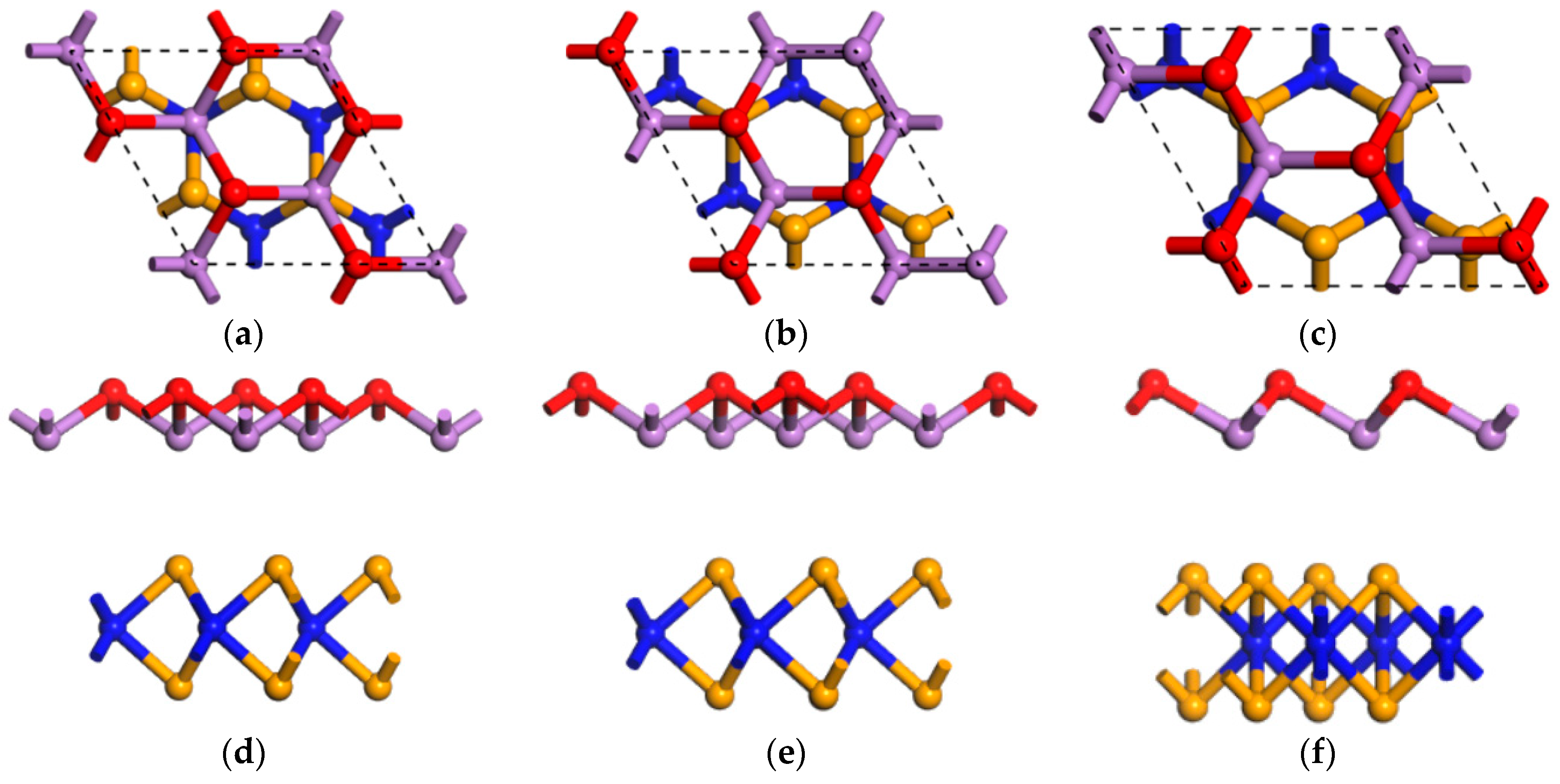
3.1. Geometric Structure of the Arsenene/WS2 Heterostructure

To theoretically model the heterostructure, we constructed the arsenene/WS2 heterostructure by stacking a 3 × 3 arsenene supercell on top of a 2 × 2 WS2 supercell. The lattice mismatch value is less than 2.5%. Meanwhile, in order to investigate the stacking effect on the arsenene/WS2 heterostructure, we consider three representative stacking configurations, namely, the bottom, top, and center configurations, which is displayed in Figure 1. Furthermore, to evaluate the structural stability of the arsenene/WS2 heterostructure, we calculated the binding energy (Eb), which can be described as follows:
E b = E A s / W E A s E W
where EAs/W, EAs, and EW are the total energies of the arsenene/WS2 heterostructure, arsenene, and monolayer WS2, respectively. Table 1 shows that the binding energies of the bottom, top, and center configurations are −746.13 meV, −751.20 meV, and −743.93 meV, respectively, which implies that all the stacking configurations are energetically stable. Based on the binding energy listed in Table 1, the trend of stability is top > bottom > center, indicating that top stacking is the most stable stacking configuration. Meanwhile, top stacking has the shortest interlayer distance of 3.28 Å. The shorter interlayer distance demonstrates a stronger vdW interaction between arsenene and WS2, which may bring about new electronic properties in the arsenene/WS2 heterostructure. Consequently, we will only discuss top stacking below.

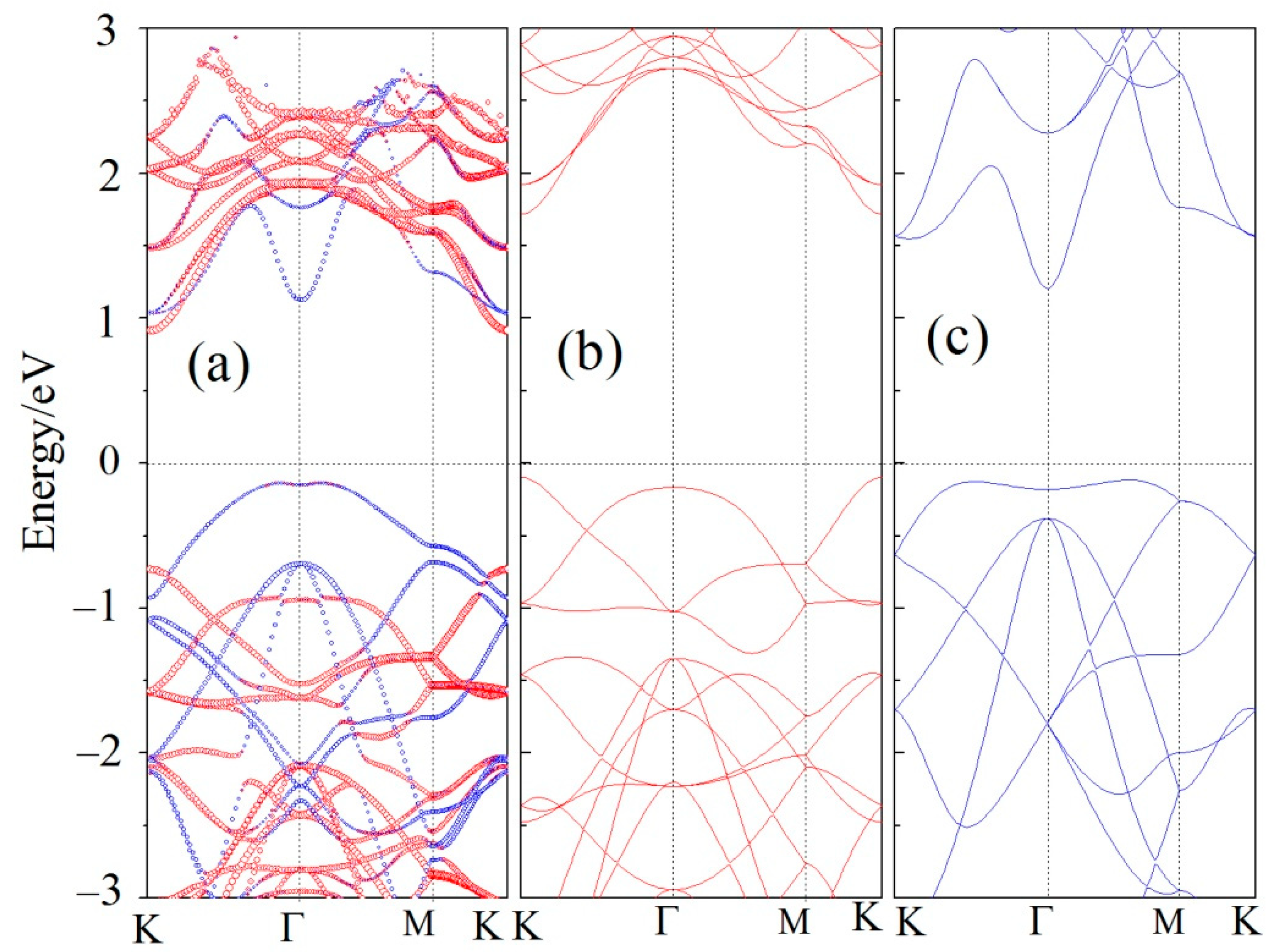
3.2. Electronic Properties of the Arsenene/WS2 Heterostructure

Here, we calculated the band structure of arsenene, monolayer WS2, and the arsenene/WS2 heterostructure, which is plotted in Figure 2. For arsenene, as depicted in Figure 2c, the conduction band minimum (CBM) lies at the Γ point and the valence band maximum (VBM) lies at the area between the M and Γ points, indicating an indirect band structure with a gap value of 1.32 eV. In the monolayer WS2, both the VBM and CBM lie at the K point; thus, a direct gap value of 1.82 eV was obtained. After the arsenene and monolayer WS2 have been combined, Figure 2a shows the band structure of the arsenene/WS2 heterostructure. In Figure 2a, the blue and red lines represent the bands of arsenene and WS2, respectively. Compared with Figure 2b,c, the band shapes of arsenene and WS2 in the heterobilayer have hardly changed, which is the simple sum of the WS2 and arsenene bands. Moreover, the CBM that is located at point K arises from WS2 and the VBM, located at the point between the Γ and M points, and originates from arsenene. Therefore, the arsenene/WS2 heterostructure possesses a type-II band alignment characteristic, which can spontaneously separate the electrons and holes in the heterostructure.
Notably, band alignment plays a key role in the performance of nanoelectronic devices; thus, we have plotted the band alignment of monolayers and the arsenene/WS2 heterostructure in Figure 3. It can be seen that the work functions of arsenene, monolayer WS2, and the arsenene/WS2 heterostructure are 5.55 eV, 5.58 eV, and 5.17 eV, respectively. When arsenene and monolayer WS2 are combined, electrons transfer from arsenene to the WS2 layer because of the larger work function of WS2. Thus, the Fermi level of arsenene (WS2) moves downward (upward) and finally comes up to the same level. Consequently, arsenene accumulates a positive charge while WS2 gathers a negative charge, which brings about an intrinsic electric field in the heterostructure. Such an intrinsic electric field can confine holes and electrons to the arsenene layer and WS2 layer, respectively. This spontaneous separation delays the recombination of electrons and holes, which prolongs the lifetime of carriers in the heterostructure.

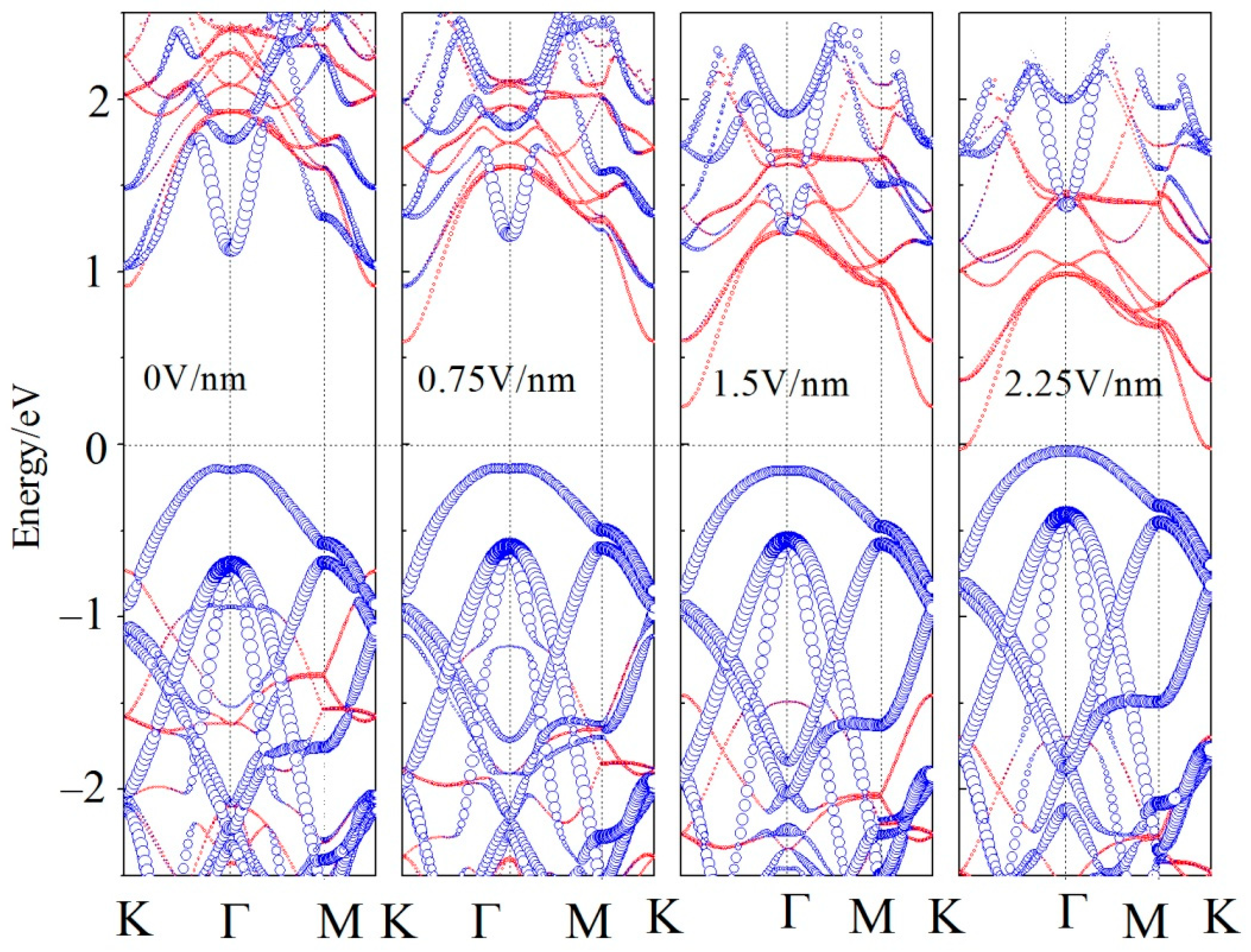
3.3. Influence of the Electric Field on Electronic Properties

It is very important to study the tunable electronic properties of the arsenene/WS2 heterojunction, due to the remarkable effect of material properties on the performance of devices. Here, we explore the band structure of the arsenene/WS2 heterojunction under various electric fields, as is demonstrated in Figure 4. The positive electric field is taken as that from WS2 to arsenene. As can be seen in Figure 4, the larger the electric field is, the smaller the band gap; eventually, the band gap reaches zero. At 0 V/nm, the arsenene/WS2 heterojunction is an indirect band gap and type-II semiconductor. When the electric field is applied to the arsenene/WS2 heterostructure, the CBM is always at point K, while the VBM moves to the Γ point, which indicates that the arsenene/WS2 heterostructure remains an indirect band-gap characteristic. It is clear that the electric field that drives the CBM shifts downward quickly, relative to the Fermi level; however, the VBM moves upward slowly, relative to the Fermi level. Ultimately, the band gap is closed at 2.25 V/nm.
To further explore the mechanism of the electric field effect on the band alignment of the arsenene/WS2 heterostructure, we present the variations in band edge under an electric field in Figure 5. Figure 5 demonstrates that the CBM and VBM of arsenene increase continuously under a positive electric field, whereas the CBM and VBM of WS2 decrease continuously. A positive electric field promotes the electron transfer from arsenene to WS2, moving the bands of arsenene upward, and that of WS2 downward. It should be noted that the CBM of WS2 is always higher than the VBM of arsenene under a positive electric field, which demonstrates that the arsenene/WS2 heterostructure remains in a type-II band alignment. Conversely to a positive electric field, a negative electric field drives the electron transfer from WS2 to arsenene, shifting the bands of WS2 upward and that of arsenene downward. Once the negative electric field is larger than −0.38 V/nm, this stronger negative electric field makes the CBM of arsenene shift down to be located below that of WS2. Meanwhile, the VBM of arsenene lies above that of WS2, where both the CBM and VBM of the heterostructure are contributed by arsenene. Therefore, the arsenene/WS2 heterostructure transforms from a type-II band alignment into a type-I band alignment at −0.38 V/nm. With the further enhancement of the negative electric field, the VBM of WS2 moves upward and is located above that of arsenene, whereas the CBM of the heterostructure can be attributed to the arsenene layer; type-II band alignment is constructed again at −0.95 V/nm. Thus, our work demonstrates that an electric field can effectively tune the band alignment types of an arsenene/WS2 heterostructure, which offers a building block for fabricating multi-functional nanoelectronic devices.

3.4. The Effect of Strain on Electronic Properties

It is necessary to study the strain effect on the electronic structures of the arsenene/WS2 heterojunction, owing to the widespread strain seen in experiments. Firstly, we apply the out-of-plane strain to the arsenene/WS2 heterojunction. Strain can be described as ε = ( d d 0 ) / d 0 , where d and d0 are the strained and unstrained interlayer distances, respectively. As can be seen from Figure 6a, the band gap decreases steadily; eventually, gap-closing occurs at −33% strain. This is because the smaller interlayer distance results in a stronger interaction in the heterostructure, which leads to more transferred charge. The Bader charge analysis shows that 0.048, 0.097, 0.1606, and 0.2962 electrons flow from arsenene to WS2, with strains of 0%, −10%, −20%, and −30%, respectively. Therefore, greater charge transfer can bring about a stronger internal electric field, which decreases the band gap of the heterostructure. Conversely, positive strain drives the band gap increases gradually. This can be attributed to the fact that the interaction became weak and transferred electrons declined with the increasing interlayer distance. The Bader charge analysis demonstrates that 0.048, 0.031, 0.024, and 0.015 electrons transfer from arsenene to WS2, with strains of 0%, 10%, 20%, and 30%, respectively. Less charge transfer means less of a wave function overlap of adjacent single layers, which narrows the energy band and then increases the band gap.
Figure 6b gives the band edge of the arsenene/WS2 heterostructure under various out-of-plane strains. It is clear that the CBM of WS2, the VBM of WS2, and the CBM of arsenene shift upward quickly with positive strain; however, the VBM of arsenene moves upward slowly. Conversely, when negative strain is applied to the heterostructure, the CBM of WS2, the VBM of WS2, and the CBM of arsenene move down quickly, whereas the VBM of arsenene shifts upward slightly. Whether a positive strain or negative strain is applied, the CBM and VBM of arsenene are always higher than that of WS2, and the type-II; band alignment of the arsenene/WS2 heterostructure is robust under out-of-plane strain.
Finally, we would like to point out that a strain above 15% could barely be achieved, while it is acceptable to present an interlayer distance with a strain of 20–30%. Related studies [43,44,45] demonstrate that the strain based on interlayer distance can exceed 30%. Moreover, it should be noticed that the interlayer distance of the WS2/MoS2 heterostructure could be modulated by vacuum thermal annealing [46]. Therefore, we can expect that the interlayer distance of the vdW heterostructures can be tuned by certain experimental methods in the future.

4. Conclusions

In conclusion, we have explored the electronic properties of the arsenene/WS2 heterostructure under electric fields and strains by means of first-principles calculations. The results demonstrate that the most stable stacking order is the top conformation of the three configurations. The negative binding energy indicates the thermodynamic stability of the arsenene/WS2 heterostructure. The band gap is effectively tuned by the electric field and, ultimately, the gap is closed. In particular, the electric field can modulate the band edges of the arsenene/WS2 heterostructure and can result in a transition between type-II and type-I band alignment. The band gap can be controlled by the strain, while type-II; band alignment is robust under strain. Our work indicates that the arsenene/WS2 heterojunction is a building block for fabricating optoelectronic and nanoelectronic devices.

Author Contributions

W.L. conceived and directed the project. F.Z. performed the calculations. L.S. created all the figures. F.Z. and X.D. drafted the paper. All authors participated in the discussion and interpretation of the results. All authors have read and agreed to the published version of the manuscript.

Funding

This research received no external funding.

Data Availability Statement

Not applicable.

Acknowledgments

We acknowledge the support from the National Natural Science Foundation of China (Grant No. 62074053).

Conflicts of Interest

The authors declare no conflict of interest.

References

  1. Geim, A.K.; Novoselov, K.S. The rise of graphene. Nat. Mater. 2007, 6, 183–191. [Google Scholar] [CrossRef] [PubMed]
  2. Zhao, X.; Xia, C.X.; Wang, T.X.; Dai, X.Q. Electronic and magnetic properties of X-doped (X = Ti, Zr, Hf) tungsten disulphide monolayer. J. Alloys Compd. 2016, 654, 574–579. [Google Scholar] [CrossRef]
  3. Schwierz, F. Graphene transistors. Nat. Nanotechnol. 2010, 5, 487–496. [Google Scholar] [CrossRef] [PubMed]
  4. Radisavljevic, B.; Radenovic, A.; Brivio, J.; Giacometti, V.; Kis, A. Single-layer MoS2 transistors. Nat. Nanotechnol. 2011, 6, 147–150. [Google Scholar] [CrossRef] [PubMed]
  5. Zhao, X.; Chen, P.; Xia, C.X.; Wang, T.X.; Dai, X.Q. Electronic and magnetic properties of n-type and p-doped MoS2 monolayers. RSC Adv. 2016, 6, 16772–16778. [Google Scholar] [CrossRef]
  6. Gong, C.; Zhang, H.; Wang, W.; Colombo, L.; Wallace, R.M.; Cho, K. Band alignment of two-dimensional transition metal dichalcogenides: Application in tunnel field effect transistors. Appl. Phys. Lett. 2013, 103, 053513. [Google Scholar] [CrossRef]
  7. Roy, T.; Tosun, M.; Kang, J.S.; Sachid, A.B.; Desai, S.B.; Hettick, M.; Hu, C.C.; Javey, A. Field-Effect Transistors Built from All Two-Dimensional Material Components. ACS Nano 2014, 8, 6259–6264. [Google Scholar] [CrossRef]
  8. Koppens, F.H.L.; Mueller, T.; Avouris, P.; Ferrari, A.C.; Vitiello, M.S.; Polini, M. Photodetectors based on graphene, other two-dimensional materials and hybrid systems. Nat. Nanotechnol. 2014, 9, 780–793. [Google Scholar] [CrossRef]
  9. Hu, P.; Wen, Z.; Wang, L.; Tan, P.; Xiao, K. Synthesis of Few-Layer GaSe Nanosheets for High Performance Photodetectors. ACS Nano 2012, 6, 5988–5994. [Google Scholar] [CrossRef]
  10. Zhu, Z.; Guan, J.; Tomanek, D. Strain-induced metal-semiconductor transition in monolayers and bilayers of gray arsenic: A computational study. Phys. Rev. B 2015, 91, 161404. [Google Scholar] [CrossRef] [Green Version]
  11. Li, W.; Wang, T.X.; Dai, X.Q.; Wang, X.L.; Ma, Y.Q.; Chang, S.S.; Tang, Y.N. Tuning the Schottky barrier in the arsenene/graphene van der Waals heterostructures by electric field. Physica E 2017, 88, 6–10. [Google Scholar] [CrossRef]
  12. Zhang, S.; Yan, Z.; Li, Y.; Chen, Z.; Zeng, H. Atomically Thin Arsenene and Antimonene: Semimetal–Semiconductor and Indirect–Direct Band-Gap Transitions. Angew. Chem. 2015, 127, 3155–3158. [Google Scholar] [CrossRef]
  13. Shah, J.; Wang, W.; Sohail, H.M.; Uhrberg, R.I.G. Experimental evidence of monolayer arsenene: An exotic 2D semiconducting material. 2D Mater. 2020, 7, 025013. [Google Scholar] [CrossRef]
  14. Kovalska, E.; Antonatos, N.; Luxa, J.; Sofer, Z. “Top-down” Arsenene Production by Low-Potential Electrochemical Exfoliation. Inorg. Chem. 2020, 59, 11259–11265. [Google Scholar] [CrossRef] [PubMed]
  15. Hu, Y.; Wang, X.Z.; Qi, Z.H.; Wan, S.S.; Liang, J.C.; Jia, Q.Q.; Hong, D.C.; Tian, Y.X.; Ma, J.; Tie, Z.X.; et al. Wet Chemistry Vitrification and Metal-to-Semiconductor Transition of 2D Gray Arsenene Nanoflakes. Adv. Funct. Mater. 2021, 31, 2106529. [Google Scholar] [CrossRef]
  16. Zhang, S.; Xie, M.; Li, F.; Yan, Z.; Li, Y.; Kan, E.; Liu, W.; Chen, Z.; Zeng, H. Semiconducting Group 15 Monolayers: A Broad Range of Band Gaps and High Carrier Mobilities. Angew. Chem. Int. Ed. 2016, 55, 1666–1669. [Google Scholar] [CrossRef]
  17. Kecik, D.; Durgun, E.; Ciraci, S. Optical properties of single-layer and bilayer arsenene phases. Phys. Rev. B 2016, 94, 205410. [Google Scholar] [CrossRef]
  18. Wang, Y.; Ding, Y. Unexpected buckled structures and tunable electronic properties in arsenic nanosheets: Insights from first-principles calculations. J. Phys. Condens. Matter. 2015, 27, 225304. [Google Scholar] [CrossRef]
  19. Zhang, Z.Y.; Cao, H.N.; Zhang, J.C.; Wang, Y.H.; Xue, D.S.; Si, M.S. Orientation and strain modulated electronic structures in puckered arsenene nanoribbons. AIP Adv. 2015, 5, 067117. [Google Scholar] [CrossRef]
  20. Tang, W.C.; Sun, M.L.; Ren, Q.Q.; Wang, S.K.; Yu, J. Halogenated arsenenes as Dirac materials. Appl. Surf. Sci. 2016, 376, 286–289. [Google Scholar] [CrossRef]
  21. Zhou, X.D.; Feng, W.X.; Li, F.; Yao, Y.G. Large magneto-optical effects in hole-doped blue phosphorene and gray arsenene. Nanoscale 2017, 9, 17405–17414. [Google Scholar] [CrossRef] [PubMed]
  22. Pan, D.; Wang, L.; Li, Z.; Geng, B.; Zhang, C.; Zhan, J.; Yin, L.; Wang, L. Synthesis of graphene quantum dot/metal–organic framework nanocomposites as yellow phosphors for white light-emitting diodes. New J. Chem. 2018, 42, 5083–5089. [Google Scholar] [CrossRef]
  23. Jia, S.; Sun, H.D.; Du, J.H.; Zhang, Z.K.; Zhang, D.D.; Ma, L.P.; Chen, J.S.; Ma, D.G.; Cheng, H.M.; Ren, W.C. Graphene oxide/graphene vertical heterostructure electrodes for highly efficient and flexible organic light emitting diodes. Nanoscale 2016, 8, 10714–10723. [Google Scholar] [CrossRef] [PubMed]
  24. Mouri, S.; Miyauchi, Y.; Matsuda, K. Tunable Photoluminescence of Monolayer MoS2 via Chemical Doping. Nano Lett. 2013, 13, 5944–5948. [Google Scholar] [CrossRef]
  25. Cheng, Y.C.; Guo, Z.B.; Mi, W.B.; Schwingenschlogl, U. Prediction of two-dimensional diluted magnetic semiconductors: Doped monolayer MoS2 systems. Phys. Rev. B 2013, 87, 100401. [Google Scholar] [CrossRef]
  26. Lu, N.; Guo, H.; Li, L.; Dai, J.; Wang, L.; Mei, W.N.; Wu, X.; Zeng, X.C. MoS2/MX2 heterobilayers: Bandgap engineering via tensile strain or external electrical field. Nanoscale 2014, 6, 2879–2886. [Google Scholar] [CrossRef]
  27. Liu, Q.; Li, L.; Li, Y.; Gao, Z.; Chen, Z.; Lu, J. Tuning Electronic Structure of Bilayer MoS2 by Vertical Electric Field: A First-Principles Investigation. J. Phys. Chem. C 2012, 116, 21556–21562. [Google Scholar] [CrossRef]
  28. Pontes, R.B.; Miwa, R.H.; da Silva, A.J.R.; Fazzio, A.; Padilha, J.E. Layer-dependent band alignment of few layers of blue phosphorus and their van der Waals heterostructures with graphene. Phys. Rev. B 2018, 97, 235419. [Google Scholar] [CrossRef]
  29. Huo, N.; Wei, Z.; Meng, X.; Kang, J.; Wu, F.; Li, S.S.; Wei, S.H.; Li, J. Interlayer coupling and optoelectronic properties of ultrathin two-dimensional heterostructures based on graphene, MoS2 and WS2. J. Mater. Chem. C 2015, 3, 5467–5473. [Google Scholar] [CrossRef]
  30. Lan, C.Y.; Li, C.; Wang, S.; He, T.Y.; Zhou, Z.F.; Wei, D.P.; Guo, H.Y.; Yang, H.; Liu, Y. Highly responsive and broadband photodetectors based on WS2–graphene van der Waals epitaxial heterostructures. J. Mater. Chem. C 2017, 5, 1494–1500. [Google Scholar] [CrossRef]
  31. Sheng, Y.W.; Xu, W.S.; Wang, X.C.; He, Z.Y.; Rong, Y.M.; Warner, J.H. Mixed multilayered vertical heterostructures utilizing strained monolayer WS2. Nanoscale 2016, 8, 2639–2647. [Google Scholar] [CrossRef] [PubMed]
  32. Lan, C.Y.; Li, C.; Wang, S.; Yin, Y.; Guo, H.Y.; Liu, N.S.; Liu, Y. ZnO–WS2 heterostructures for enhanced ultra-violet photodetectors. RSC Adv. 2016, 6, 67520–67524. [Google Scholar] [CrossRef]
  33. Wang, M.; Gao, L.; Yu, P.X.; Wang, Q.; Yu, C.X.; Zhang, X.Y.; Wang, Y.H.; Zheng, W.T.; Zhang, J.Q. Synergetic interfacial passivation, band alignment, and long-term stability with halide-optimized CsPbBrxI3−x nanocrystals for high-efficiency MAPbI3 solar cells. J. Mater. Chem. C 2022, 10, 5134–5140. [Google Scholar] [CrossRef]
  34. Fan, C.; Yang, K.; Xu, X.; Qi, Z.D.; Jiang, S.; Xia, M.X.; Zhang, Q.L. Controllable vapor growth of CsPbBr3/CdS 1D heterostructures with type-II band alignment for high-performance self-powered photodetector. CrystEngComm 2022, 24, 275–283. [Google Scholar] [CrossRef]
  35. Peng, P.; Milliron, D.J.; Hughes, S.M.; Johnson, J.C.; Alivisatos, A.P.; Saykally, R.J. Femtosecond Spectroscopy of Carrier Relaxation Dynamics in Type II CdSe/CdTe Tetrapod Heteronanostructures. Nano Lett. 2005, 5, 1809–1813. [Google Scholar] [CrossRef]
  36. Wang, Z.; Yin, H.; Jiang, C.; Safdar, M.; He, J. ZnO/ZnSxSe1−x/ZnSe double-shelled coaxial heterostructure: Enhanced photoelectrochemical performance and its optical properties study. Appl. Phys. Lett. 2012, 101, 253109. [Google Scholar] [CrossRef]
  37. Wang, F.; Wang, Z.; Xu, K.; Wang, F.; Wang, Q.; Huang, Y.; Yin, L.; He, J. Tunable GaTe-MoS2 van der Waals p–n Junctions with Novel Optoelectronic Performance. Nano Lett. 2015, 15, 7558–7566. [Google Scholar] [CrossRef]
  38. Cao, T.; Luo, L.T.; Huang, Y.F.; Ye, B.; She, J.C.; Deng, S.Z.; Chen, J.; Xu, N.S. Integrated ZnO Nano-Electron-Emitter with Self-Modulated Parasitic Tunneling Field Effect Transistor at the Surface of the p-Si/ZnO Junction. Sci. Rep. 2016, 6, 33983. [Google Scholar] [CrossRef]
  39. Blöchl, P.E. Projector augmented-wave method. Phys. Rev. B 1994, 50, 17953. [Google Scholar] [CrossRef]
  40. Grimme, S. Semiempirical GGA-type density functional constructed with a long-range dispersion correction. J. Comput. Chem. 2006, 27, 1787–1799. [Google Scholar] [CrossRef]
  41. Kresse, G.; Furthmüller, J. Efficient iterative schemes for ab initio total-energy calculations using a plane-wave basis set. Phys. Rev. B 1996, 54, 11169. [Google Scholar] [CrossRef] [PubMed]
  42. Kerber, T.; Sierka, M.; Sauer, J. Application of semiempirical long-range dispersion corrections to periodic systems in density functional theory. J. Comput. Chem. 2008, 29, 2088–2097. [Google Scholar] [CrossRef]
  43. Hu, W.; Wang, T.; Yang, J.L. Tunable Schottky contacts in hybrid. J. Mater. Chem. C 2015, 3, 4756–4761. [Google Scholar] [CrossRef]
  44. Vu, T.V.; Hieu, N.V.; Phu, H.V.; Hieu, N.N.; Bui, H.D.; Idrees, M.; Amin, B.; Nguyen, C.V. Graphene/WSeTe van der Waals heterostructure: Controllable electronic properties and Schottky barrier via interlayer coupling and electric field. Appl. Surf. Sci. 2020, 507, 145036. [Google Scholar] [CrossRef]
  45. Nguyen, C.V. Electric gating and interlayer coupling controllable electronic structure and Schottky contact of graphene/BiI3 van derWaals heterostructure. Phys. Rev. B 2021, 103, 115429. [Google Scholar] [CrossRef]
  46. Tongay, S.; Fan, W.; Kang, J.; Park, J.; Koldemir, U.; Suh, J.; Narang, D.S.; Liu, K.; Ji, J.; Li, J.B.; et al. Tuning Interlayer Coupling in Large-Area Heterostructures with CVD-Grown MoS2 and WS2 Monolayers. Nano Lett. 2014, 14, 3185–3190. [Google Scholar] [CrossRef]
Figure 1. Top and side view of the arsenene/WS2 heterostructure: (a,b) bottom configuration; (c,d) top configuration; (e,f) center configuration. The red, purple, orange and blue balls represent the up As, bottom As, S, and W atoms, respectively.
Crystals 12 01390 g001
Figure 2. The band structure of the arsenene/WS2 heterostructure (a), WS2 (b), and arsenene (c). The blue and red lines represent the bands of arsenene and WS2, respectively.
Crystals 12 01390 g002
Figure 3. The band alignment of monolayers and the arsenene/WS2 heterostructure.
Crystals 12 01390 g003
Figure 4. The band structure of the arsenene/WS2 heterostructure under various external electric fields. The blue and red lines represent the bands of arsenene and WS2, respectively.
Crystals 12 01390 g004
Figure 5. The band edge of the arsenene/WS2 heterojunction under various electric fields. EC-WS2(As) and EV-WS2(As) are the CBM and VBM of WS2 (arsenene) in the arsenene/WS2 heterojunction.
Crystals 12 01390 g005
Figure 6. The band gap (a) and band edge (b) of the arsenene/WS2 heterostructure under various out-of-plane strains. EC-WS2(As) and EV-WS2(As) are the CBM and VBM of WS2 (arsenene) in the arsenene/WS2 heterojunction.
Crystals 12 01390 g006
Table 1. The interlayer distance, D, and binding energy, Eb, of the arsenene/WS2 heterostructure for three stacking configurations.
StackingBottomTopCenter
D (Å)3.313.283.32
Eb (meV)−746.13−751.20−743.93
Publisher’s Note: MDPI stays neutral with regard to jurisdictional claims in published maps and institutional affiliations.

