Article

Spin-Polarized Study of the Structural, Optoelectronic, and Thermoelectric Properties of the Melilite-Type Gd2Be2GeO7 Compound

1
Laboratoire d’Etude des Matériaux et Instrumentations Optiques (LEMIO), Université Djillali Liabès de Sidi Bel-Abbès, Sidi Bel-Abbès 22000, Algeria
2
Condensed Matter and Sustainable Development Laboratory (LMCDD), Université Djillali Liabès de Sidi Bel-Abbès, Sidi Bel-Abbès 22000, Algeria
3
Laboratoire d’Elaboration et de Caractérisation des Matériaux (LECM), Université Djillali Liabès de Sidi Bel-Abbès, Sidi Bel-Abbès 22000, Algeria
4
Laboratoire de Physique Quantique de la Matière et de Modélisation Mathématique (LPQ3M), Université de Mascara, Mascara 29000, Algeria
5
Department of Physics and Astronomy, College of Science, King Saud University, P.O. Box 2455, Riyadh 11451, Saudi Arabia
6
Laboratory for Developing New Materials and Their Characterizations, Department of Physics, Faculty of Science, University of Ferhat Abbes-Setif 1, Setif 19000, Algeria
7
Department of Physics, College of Science, King Faisal University, P.O. Box 400, Al-Ahsa 31982, Saudi Arabia
8
College of Science, Physics Department, Alfaisal University, P.O. Box 50927, Riyadh 11533, Saudi Arabia
*
Authors to whom correspondence should be addressed.
Crystals 2022, 12(10), 1397; https://doi.org/10.3390/cryst12101397
Submission received: 6 September 2022 / Revised: 25 September 2022 / Accepted: 27 September 2022 / Published: 2 October 2022
(This article belongs to the Special Issue Nanostructured Thermoelectric Materials)

Abstract

:
The present work is a theoretical study of the structural and spin-polarized dependent optoelectronic thermoelectric properties of the melilite-typeGd2Be2GeO7 compound, using the full potential linearized augmented plane wave approach in the framework of density functional theory. The predicted structural parameters are in good accordance with the measured counterparts. It is found that the title compound is more stable in the ferromagnetic order than in the non-magnetic order. The calculated band structure using the modified Becke–Johnson potential reveals that the studied compound has a wide bandgap of 3.78 eV. The frequency-dependent linear optical spectra are studied in an energy range expanding from 0 to 30 eV. Finally, the semi classical Boltzmann theory as incorporated in the Boltztrap code is used to study the spin-polarized dependent transport properties. The obtained results show that Gd2Be2GeO7 is a potential candidate for conversion energy device applications.

1. Introduction

Rare earth (RE melilite type RE2Be2GeO7 compounds (RE = Pr, Nd, Gd, Yb, Dy) crystalize in a tetragonal structure with the P 4 ¯ 2 1   m   space group. Yellow feldspar is a group of pyrosilicate compounds that may be found in high-temperature metamorphosed impure limestone and silica under soaked igneous rocks. [1,2,3]. They are employed in a variety of applications, including optical materials and fuel cell ingredients for the development of solid oxide fuel cell (SOFC) technology [4]. The 4f electrons in melilite compounds containing lanthanide atoms, in particular, are highly influenced by the surrounding coordination environment, and exhibit radically different behaviors compared with the single element. This structural characteristic has been widely used to create magnetic and optical materials with desired qualities [5,6]. Melilites have been a research focus for a long time [7,8,9] because of the ability to combine and crystallize atoms to achieve entirely new usabilities and allow the discovery of a compound with a new function. This opportunity is one of the most important contributions that solid-state chemistry field makes to society. Warren [10] was the first to determine the crystal structure of a synthesized melilite. Many different melilite compounds have been produced since then [11,12,13,14,15,16,17].
One of such compounds, the Gd2Be2GeO7melilite type compound, has attracted attention; it was previously synthesized, and its crystal structure was characterized by Ochi et al. [18]. In addition, recently, Ashtaret et al. [19] reported the synthesis, structure, and magnetic properties of this compound and other families of melilite-type RE2Be2GeO7 (RE = Pr, Nd, Dy, Yb) polycrystals using the solid-state reaction method. Few studies have highlighted the spin-polarized dependent optoelectronic and thermoelectric properties of melilite containing rare earth (RE) atoms which are considered to have a high degree of freedom of chemical composition. The discovery of new qualities resulting from the crystalline structure of the melilite-type compound was the focus of this research. The main goal of this study is to explain the spin-polarized contribution to the electronic band structure, optical response, and thermoelectric properties of Gd2Be2GeO7 compound, using the FP-LAPW method based on density functional theory [20,21,22,23,24,25]. We find that the spin-polarized calculations with the modified Beck Johnson approach [26,27,28,29] raise the important wide-band gap magnetic semiconductor behavior in this compound.
This paper is organized as follows. A general introduction to the melilite compounds is given in Section 1. We summarize the significant parameters introduced in our theoretical methods used in this study in Section 2. In Section 3, we investigate the spin-polarized dependent calculations of the crystal structures, optoelectronics, and thermoelectric properties of Gd2Be2GeO7 melilite-type compound. Furthermore, and in order to elucidate the optical coating properties, transmittance, reflectance, and absorbance at different thicknesses were performed. Concluding remarks are summarized in the last section.

2. Methodology and Calculation Settings

The full potential linear augmented plane wave (FP-LAPW) approach [22,23] based on density functional theory [20,21] as incorporated in the WIEN2k code [24] was used to investigate the structural, electronic, and magnetic characteristics of the melilite-type Gd2Be2GeO7 compound. The GGA-PBE version of the generalized-gradient approximation (GGA) [25] and the modified Becke–Johnson potential by Tran and Blaha (TB-mBJ) [26,27,28,29] were used to treat the exchange-correlation effects. The muffin-tin sphere radius was chosen to be 1.8 Bohr for Gd and Ge, 1.4 Bohr for Be, and 1.35 Bohr for O. The energy convergence criterion was set to 10−4 Ry to ensure accurate computations. The electronic configuration of each element is taken as follows: Gd: [Xe] 6s2 4f7 5d1, Be: [He] 2s2, Ge: [Ar] 4s2 3d10 4p2, and O: [He] 2s2 2p4. A dense Brillouin zone sampling of 18 × 18 × 28 k-mesh was used for the optical and thermoelectric characteristics. The transport parameters were determined through the semi classical Boltzmann theory as implemented in the BoltzTrap code [30].

3. Results and discussion

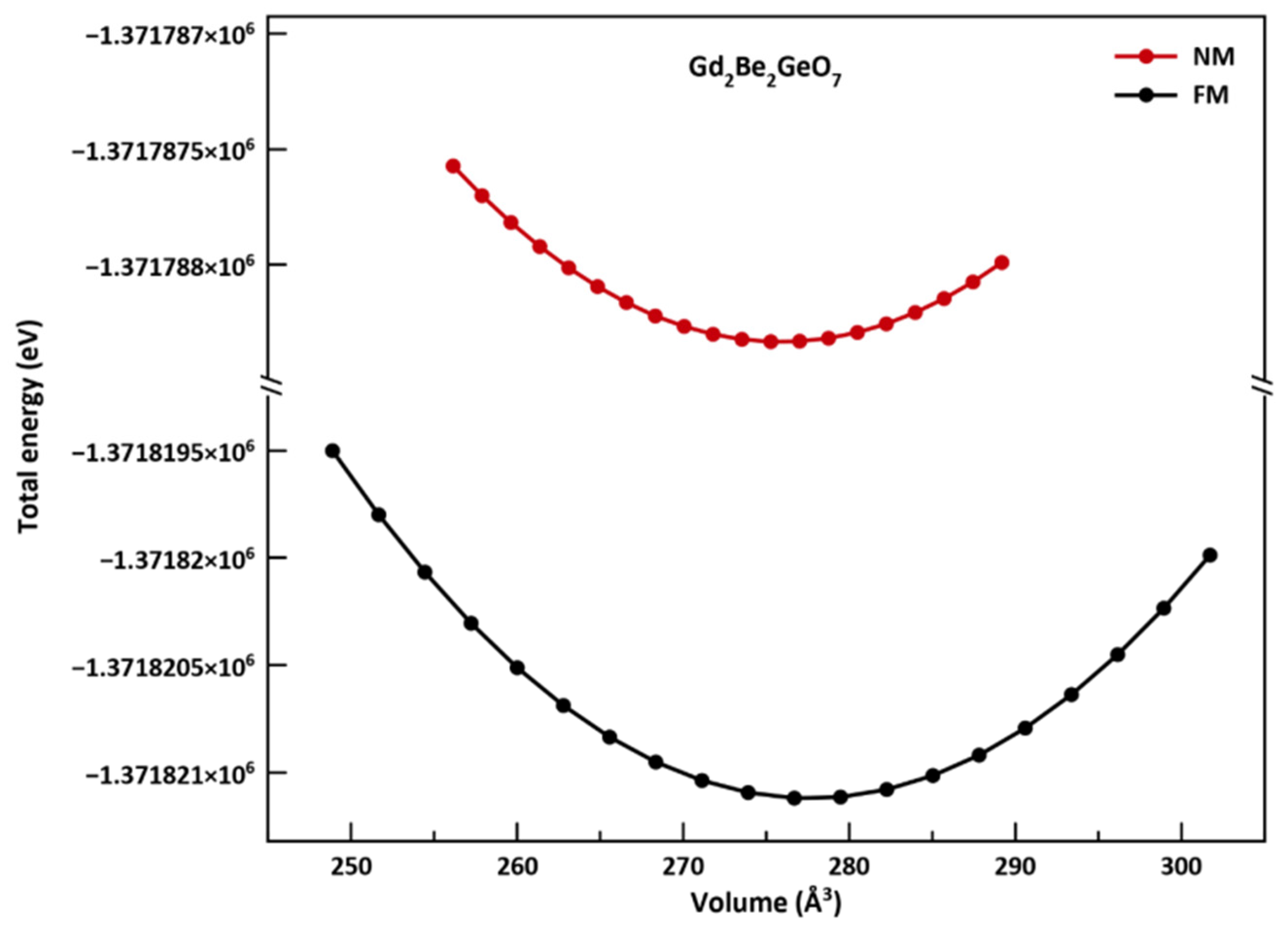
3.1. Structural Properties

Gd2Be2GeO7 is isostructural to the melilitetype group A2MM’2O7, where A symbolizes bigger cations such as alkali earth ions and lanthanides, and M and M’ denote smaller divalent to tetravalent cations. The melilite crystallizes in a tetragonal structure with space group P 4 ¯ 2 1 m (SG No13) [1,2,3,4,5,6,7,8,9,10,11,12,13,14,15,16,17,18,19], and can be represented as two-dimensional lattices in the ab-plane consisting of MO4 and M’O4 tetrahedra, with the larger A ions occupying the space between these lattices.
There are six crystallographic sites in the unit cell: one Wyckoff site 4e occupied by Gd atom, one site 2a occupied by Ge atom, one site 4e occupied by Be atom, and three Wyckoff sites 2c, 2a, 8f occupied by O atoms. Figure 1 depicts the crystal structure of melilite-type Gd2Be2GeO7. Figure 2 shows that the title compound is more stable in the ferromagnetic order than in in the non-magnetic one, so only the physical properties of Gd2Be2GeO7 in the ferromagnetic order were studied. The calculated total energy versus the volume data are fitted to the Birch–Murnaghan equation of state [31,32] and the obtained equilibrium structural parameters, such as the unit cell volume (V0), lattice parameters (a, and c), bulk modulus (B0) and its pressure derivative (B’) are summarized in Table 1. We notice that our results are very close to the reported experimental data [18,19].

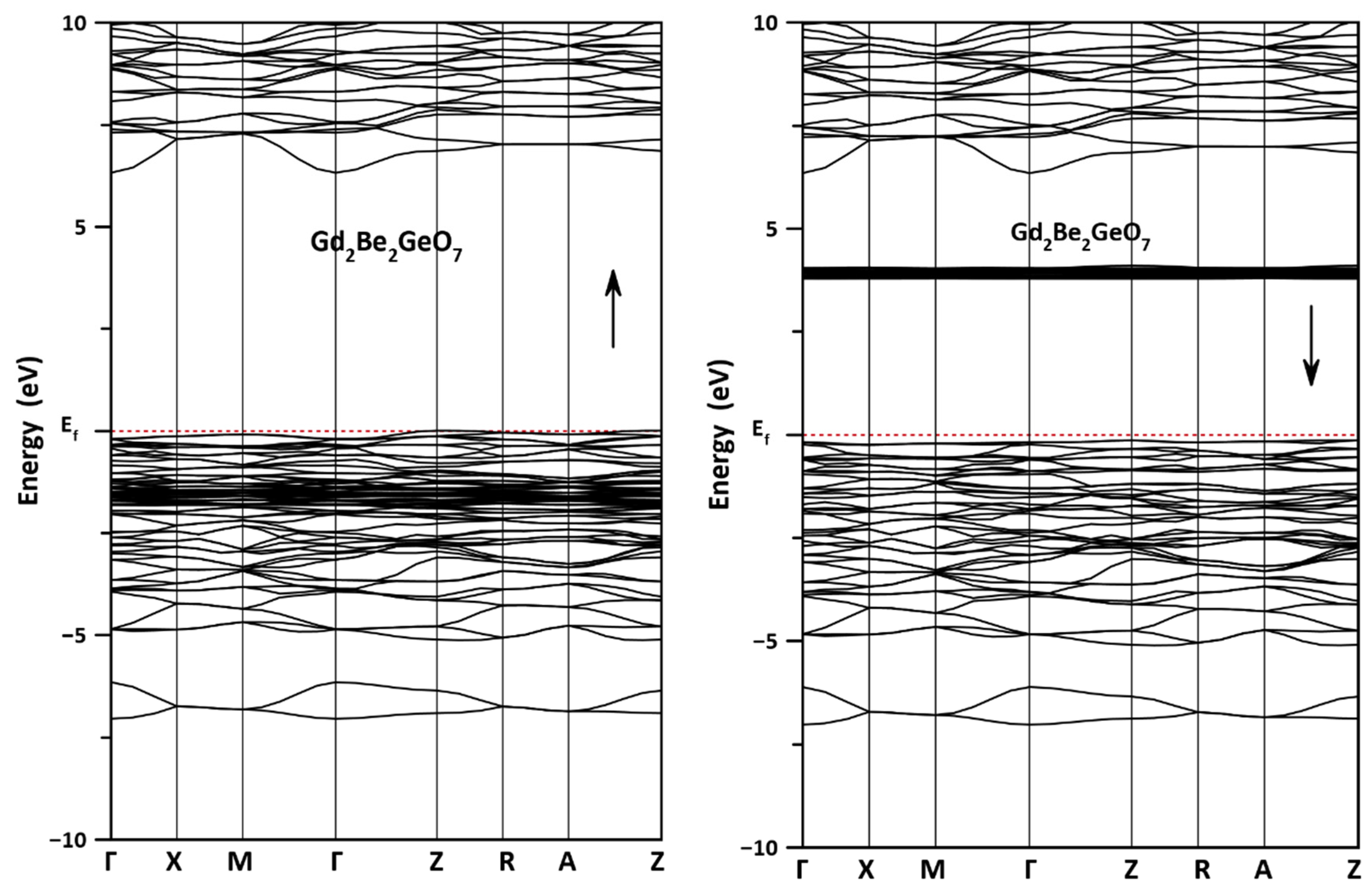
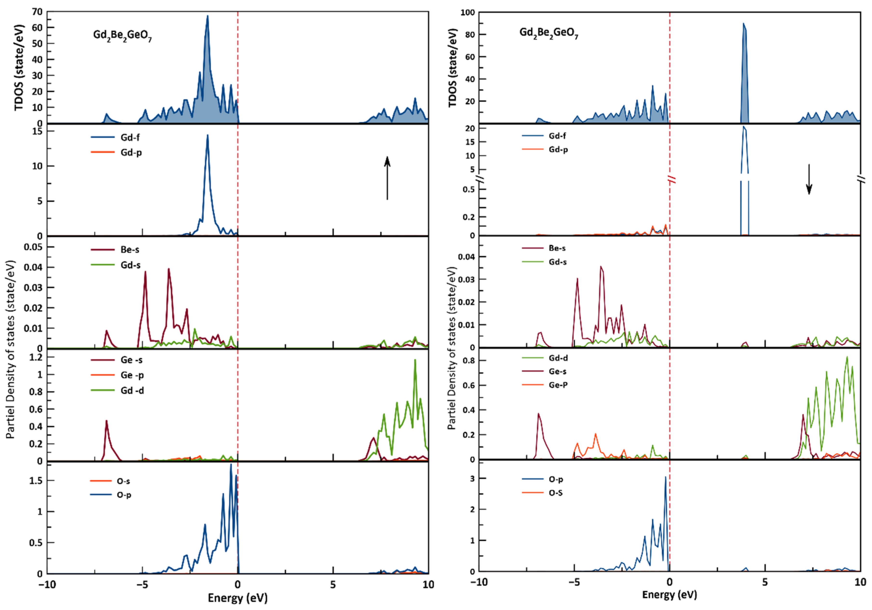
3.2. Electronic Properties

The electron energy band structure of the Gd2Be2GeO7 compound was examined at equilibrium lattice parameters, taking into consideration spin polarization, based on the stable melilite phase; the computational procedure was accomplished using PBE-GGA and PBE-GGA-mBJ techniques. This allows us to go beyond traditional GGA/LSDA methodologies and treat electron correlations more accurately, correcting the band gap and the contribution of various orbitals. The Brillouin zone of the melilite structure is represented in Figure 3, with the recommended band path taken from reference [33].
Including spin polarization with GGA-mBJ scheme, the calculated energy band dispersion and diagram of the total density of states (TDOS) of the Gd2Be2GeO7 compound are illustrated in Figure 4 and Figure 5, respectively, according to the spin-up and spin-down channels. Analysis of the obtained curves shows that this compound presents an interesting band gap behavior. First, as seen in Figure 4, the material under discussion exhibits an insulating band gap behavior with an indirect Z−Γ band gap of 6.319 eV for the majority spin, while the semiconductor behavior of this compound predominates in the minority spin with a direct band gap Z−Z of 3.928 in which the VBM is located below the Fermi level. Table 2 shows the computed values for the highest valence band (HVB) and lowest conduction band (LCB) in the tetragonal BZ for the examined Gd2Be2GeO7 material at various high-symmetry k-points. Therefore, the spin-polarized Gd2Be2GeO7 material has a direct wide-band gap (ZC − ZV) of about 3.781 eV. For the first time, these results are presented in the context of the DFT technique with the spin-polarized GGA-mBJ exchange potential for the best correction of the electronic band energies and their localizations. Figure 5 displays the atom projected density of states (PDOS) for those atomic species whose orbitals may have substantial contributions around the Fermi level, spin-up and spin-down polarizations to better understand the electronic and magnetic characteristics of Gd2Be2GeO7. The energy levels below the Fermi level are mainly consisting of Ge-4s4p, Be-2s as well as the Gd-p states. The electronic states of Be and O atoms cohere with each other throughout the area from the VB to the CB, and the states of Ge and O atoms are likewise totally overlapped, indicating that these orbitals strongly hybridize with each other due to interactions in the BeO4 and GeO4 tetrahedrons.
In addition, the occupied f states of Gadolinium fall below the O-2p valence bands, spin-up (majority), whereas unoccupied f states of Gd fall in the band gap, spin-down (minority); finally the 5d-Gdare mainly localized in the conduction band both in majority spin (spin-up) and minority spin (spin-down) channels. The obtained values of the total magnetic moment (μ) of the studied compound Gd2Be2GeO7 using spin-polarized GGA + mBJ calculations are observed around 7.497 μB, which agrees well with those found by Ochi. et al. [18] (7.94–7.20 μB) and M. Ashtar et al. [19] (7.05 μB). As seen in Table 3, most of the magnetic moments arise from the Gd-f states with small contributions from the interstitial region and the other constituent atoms.

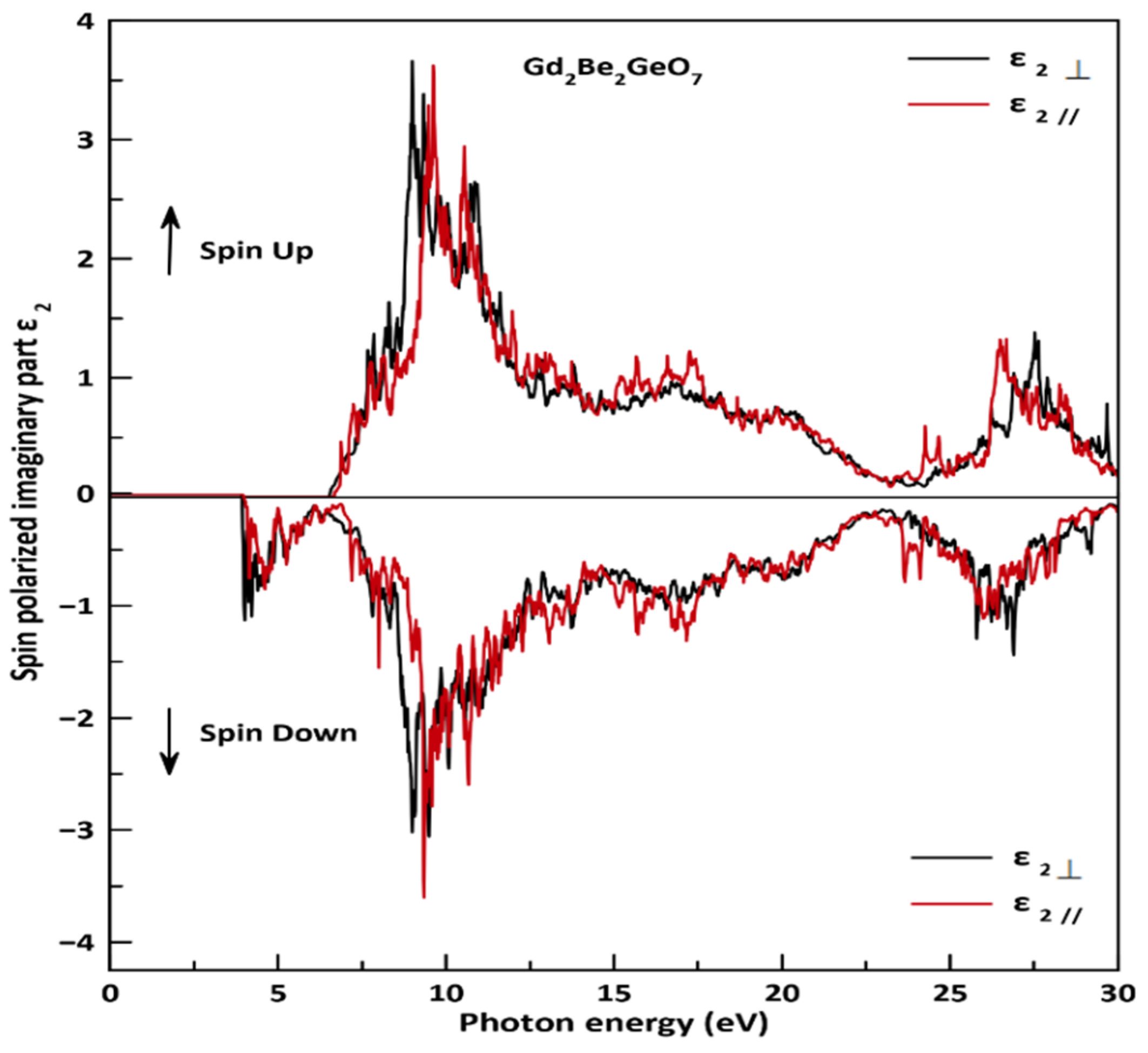
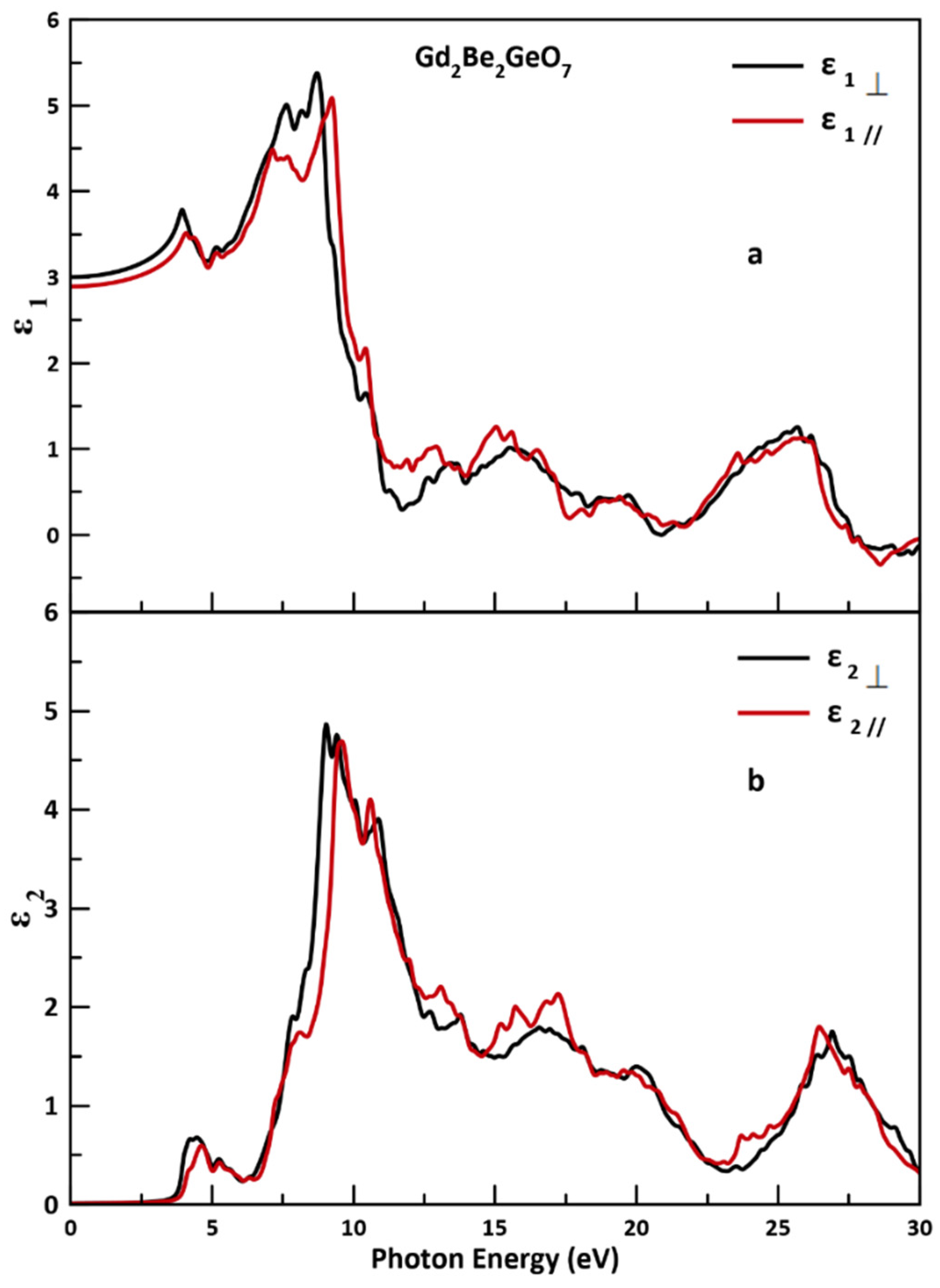
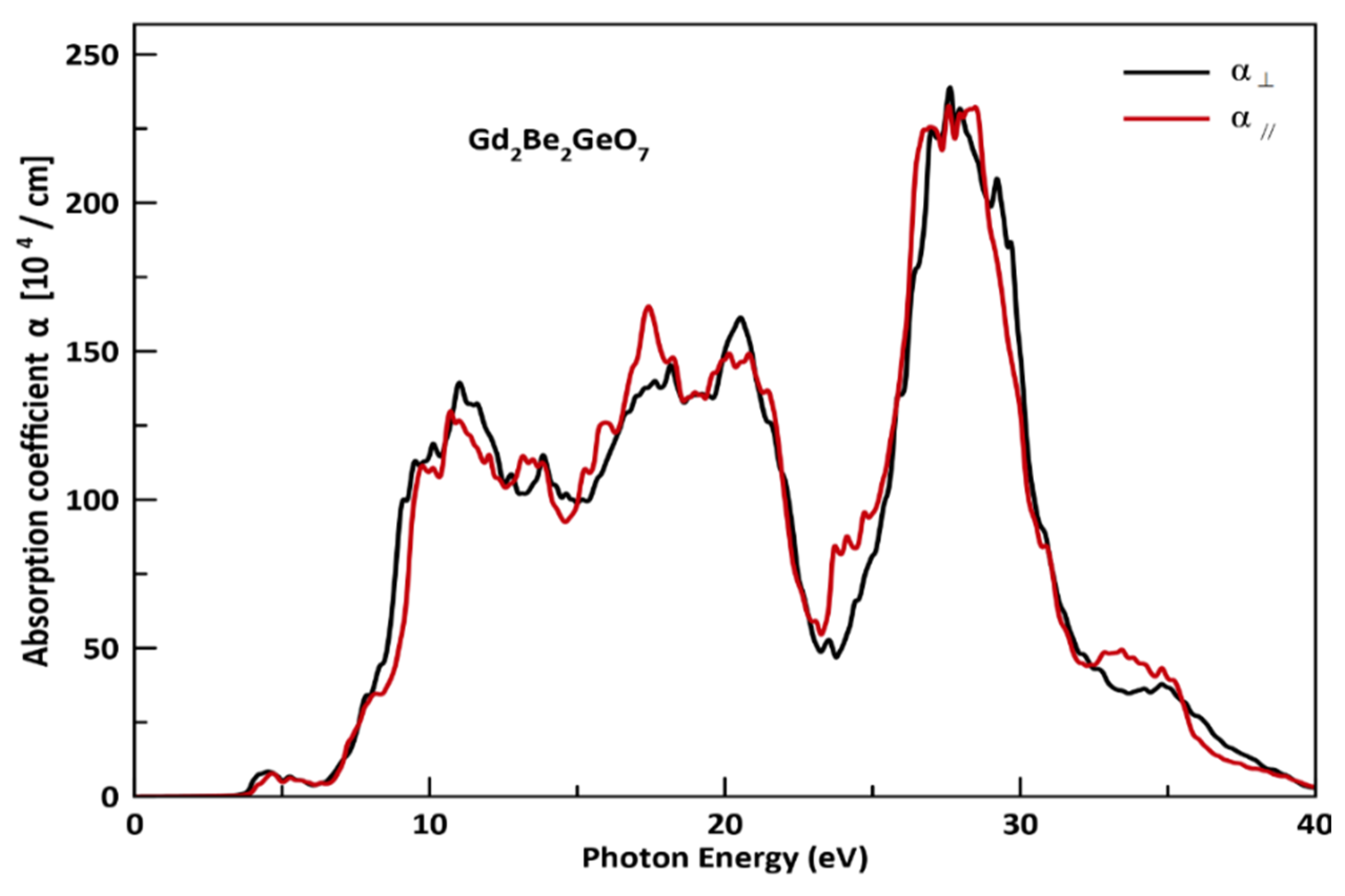
3.3. Optical Properties

Knowledge of the optical properties of materials is necessary before their implication in optoelectronic device applications. Therefore, an accurate theoretical method to assess the optical properties of materials is required. The state-of-the-art FP-LAPW method [24] with the GGA + mBJ functional [25,26] might be a good theoretical tool for the investigation of the optical properties of the melilite-type Gd2Be2GeO7 compound. Furthermore, adding spin-polarized calculations to this method, the optical properties of this compound give interesting discussion and useful information about its internal structure [34,35].
The dielectric function ε(ω) = ε1 + iε2 describes the linear response of a material to incident electromagnetic radiation, where ε1 (the real part) describes the dispersion of radiation inside the medium and ε2 (the imaginary part) describes the absorption of radiation by the medium [35,36]. All other optical coefficients, such as refractive indexes, reflectivity coefficient and absorption coefficient, can be calculated from the dielectric function through known relationships. Due to the tetragonal symmetry of the investigated material, all optical spectra are calculated for an electrical field vector E of the incident electromagnetic radiation polarized both parallel and perpendicular to the c-axis (E//c and E⊥c).
Our findings serve as a prediction because no previous study on the optoelectronic properties of the title compound has been made. Figure 6 depicts the ε2spectrum for the Gd2Be2GeO7 compound spin-up and spin-down channels in an energy range 0–30 eV. According to spin-polarized GGA + mBJ band structure computations, the compound under consideration’s valence band maximum and conduction band minimum exhibit divergent behavior, where it can be an insulator for spin-up polarization and a semiconductor for spin-down polarization. The ε2 spectra for both spin-up and spin-down channels clearly show the above characteristics. The absorption edge (the first critical point of ε2 (ω)), occurring at 3.9 eV for the minority spin channel and at 6.319 eV for the majority spin channel, is originated from the electronic transitions from the valence band maximum states to the conduction band minimum states. The band structure has a significant impact on the optical metrics given above, and our findings are consistent with the specific electronic properties outlined in the preceding section.
The ε1 (ω)spectrum was calculated from that of ε2 (ω) through the Kramers-Kronig relation [37,38]. In spin-polarized optics computations, the Kramers-Kronig (KK) transformation is not a simple additive quantity [34]. The real and imaginary components of the dielectric function as a function of photon energy are shown in Figure 7. The absorptive component ε2 (ω) describes the optical transition process between the energy bands in materials. The optical spectra of materials are formed by the electronic transitions from the highest occupied orbitals in the valence band to the lowest vacant orbitals in the conduction band. The suitable optical transitions, according to the selection rules, are s → p, p → d, d → p, d → f, and so on. In the imaginary part ε2 (ω) curve, the threshold energy of the dielectric function occurs at E0 = 3.7 eV, which corresponds to the fundamental gap at equilibrium.
It is commonly accepted that materials with band gaps higher than 3.1 eV are suitable for uses in the ultraviolet (UV) spectrum. As a result, this broad band gap material might be appropriate for UV device applications. Furthermore, in the energy range of 7.5 to 17 eV, the ε1 (ω) and ε2 (ω) spectra exhibit a strong anisotropy in both directions of polarized light (parallel E//c as well as perpendicular E⊥c to the c-axis). This optical anisotropy is predicted due to the crystal’s poor symmetry. The principal peaks of the ε2 (ω) spectra are caused by electronic transitions from the O-p occupied valence states to the Gd-f and Gd-d empty conduction states.
Figure 7a shows ε1 (ω)spectra. This function provides information about a material’s electronic polarizability. The static dielectric constant ε1 (0) values for E⊥c and E//c are 3.002 and 2.893, respectively. ε1 (ω) begins to increase from its zero frequency limit to reach a maximum value of 5.5 at 10 eV, and then drops below 0 on the negative scale for photon energy ranging from 26 to 28 eV. Figure 7b and Figure 8b show a similar trend in the behavior of ε2 (ω)and the extinction coefficient k (ω). The k (ω) threshold energy is roughly at 3.7 eV. At energies above this limit, k (ω) reaches its maximum value at 11 eV.
At higher energy, both components of the extinction coefficient show a significant drop. The refractive index (n(ω)) spectrum exhibits a noticeable anisotropy in the energy ranges 8–10 eV as can be seen in Figure 8a. The value of n(ω) becomes smaller than unity above 14 eV; this significant occurrence reflects the speed of light after passing through the substance. This effect could be beneficial in optoelectronics. The static refractive indices n(0) and n||(0) are 1.732 and 1.701, respectively, and the corresponding birefringence Δn (0) is 0.031. The absorption of photons of light determines the excitation energy of an electron for passing over the band gap of a material. ε2 (ω)is directly related to the absorption coefficient α(ω), which is defined as the amount of power absorbed when light passes through a solid. The optical absorption spectra of the described compound, as shown in Figure 9, demonstrate that it has a relatively high optical absorption (>150 cm−1) throughout a large energy range in the ultraviolet range between 5 and 20 eV. Furthermore, the absorption coefficient α (ω) has peaked at 8 eV, 10 eV and 12 eV, which correspond to the inter-band transitions and then it gradually takes the higher values at higher photon energies. Despite the fact that the discussed compound (Gd2Be2GeO7) has a wide-band gap and is structurally anisotropic; in lower photon energy region it is found to be optically isotropic, for which this feature makes it a potential candidate for the scintillator applications.

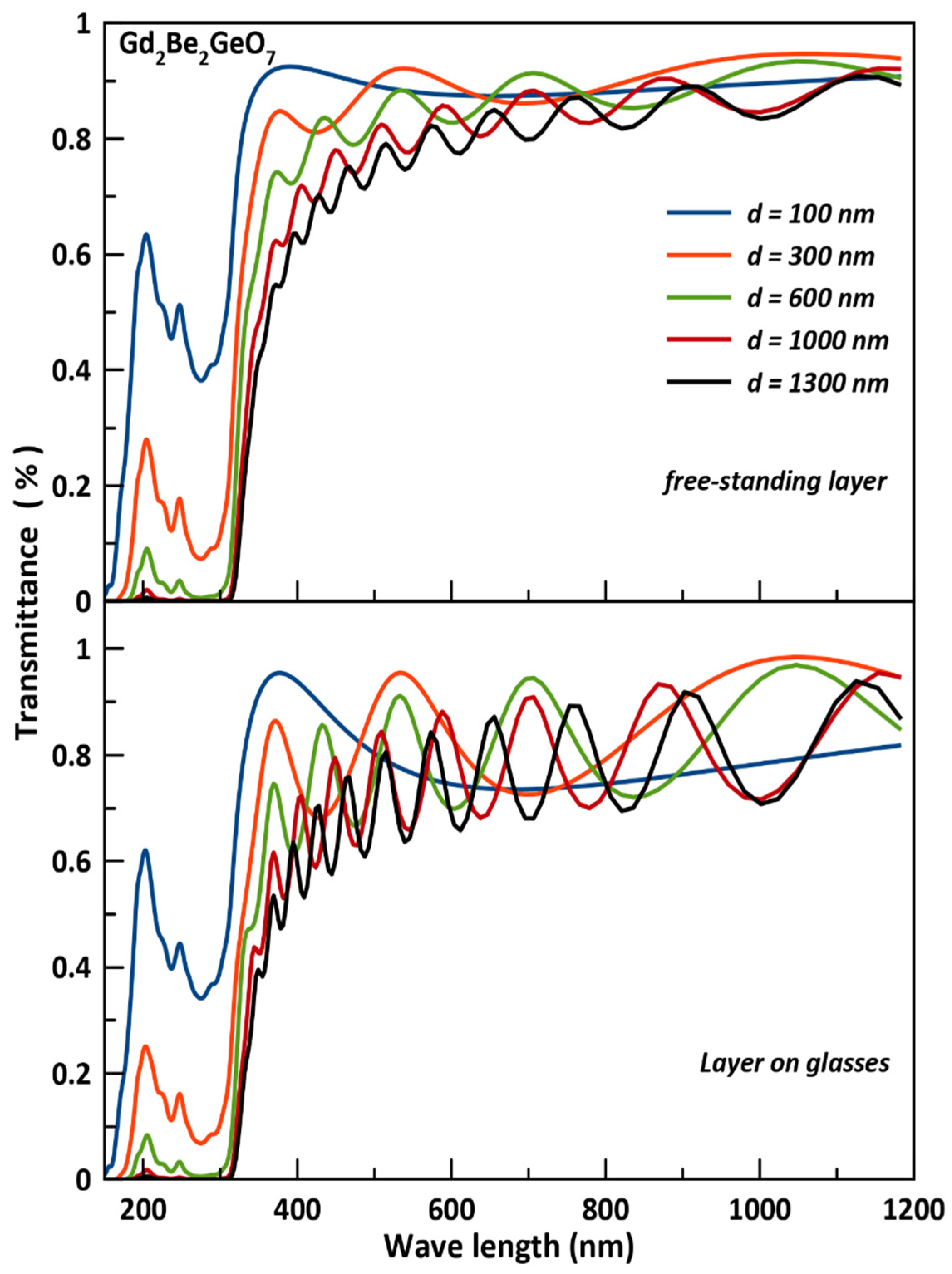
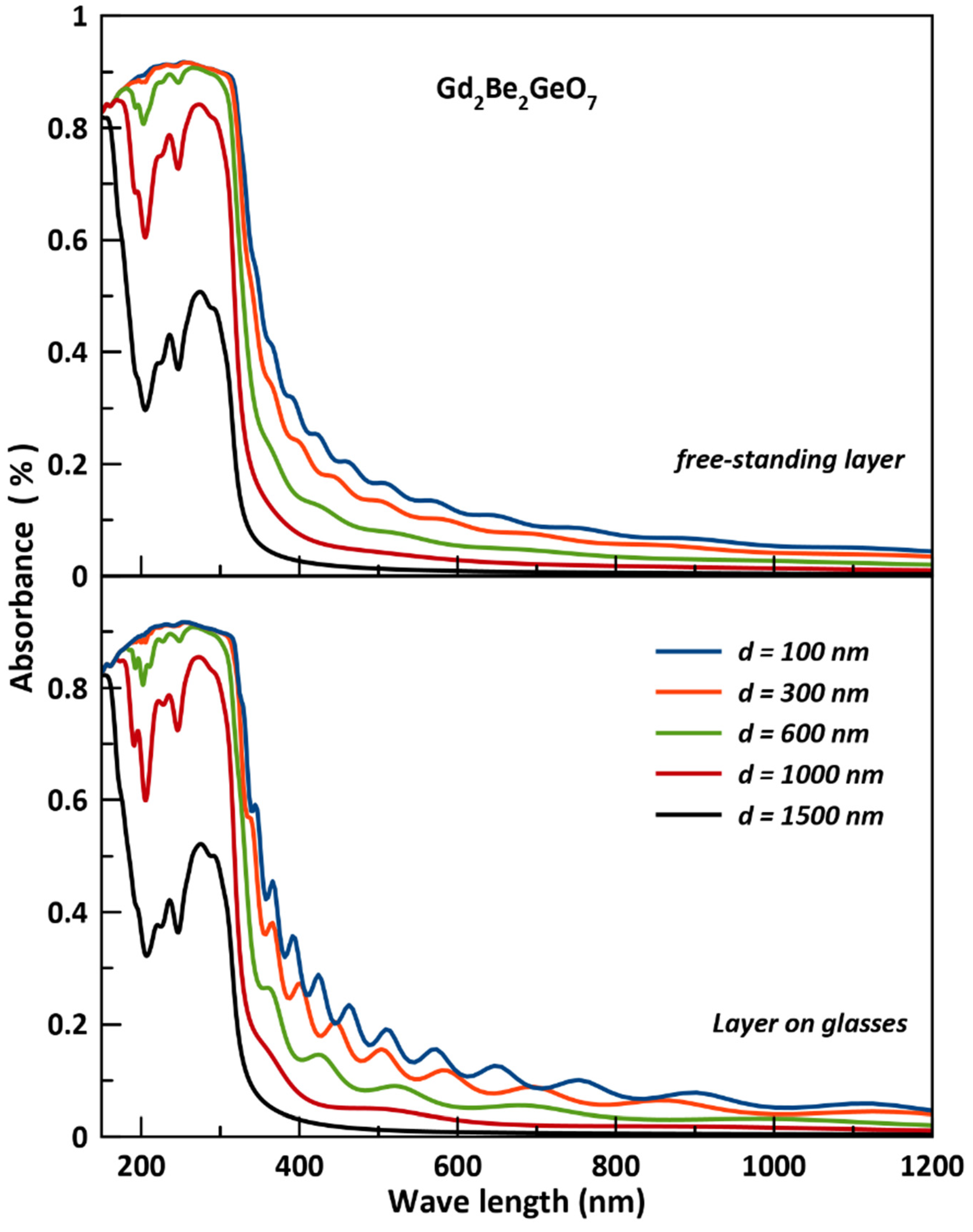
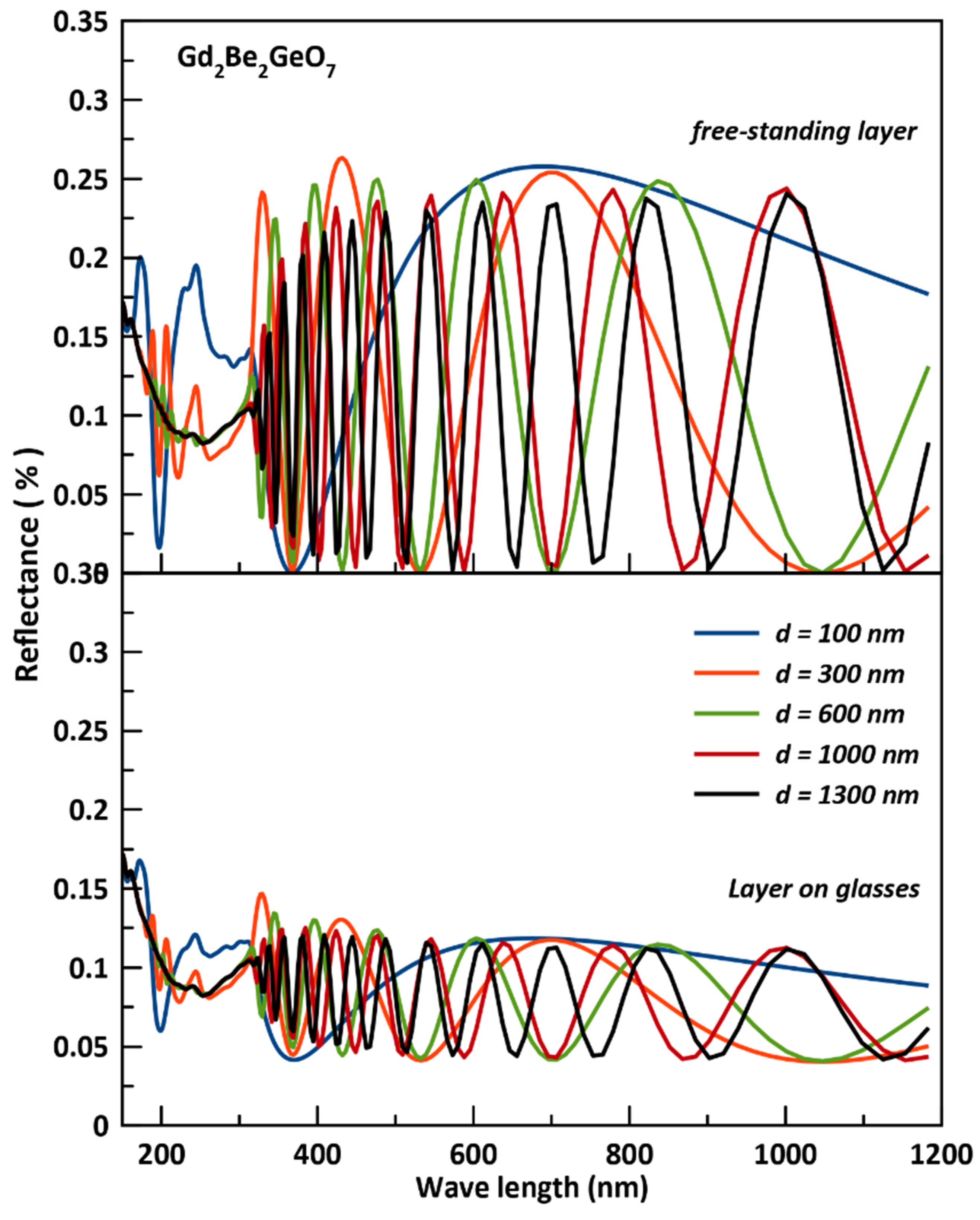
3.4. Optical Coating Characteristics

We attempted to examine the layer coating of the melilite-type compound Gd2Be2GeO7 using the optical matrix approach, which is crucial for optical thin film design programs [39,40], in order to characterize the optical properties of this material to this extent.
This method considers each layer of the material as a 2 × 2 matrix, with the previously calculated extinction coefficient and refractive index of the optical properties (Section 3.3), resulting in thin films optical properties such as transmittance, absorbance, and reflectance, which are functions of the extinction coefficient (k) and refractive index (n), as well as geometry (thickness (d), surface roughness), etc. [41,42,43,44,45,46]. Two techniques were used in the optical cladding research: one on a clear substrate (glasses: nglasses = 1.5, kglasses = 0) and the other on a free-standing layer (nair =1, kair = 0). Figure 10, Figure 11 and Figure 12 show plots of optical coating spectra of the examined Gd2Be2GeO7 thin film, such as Transmittance, Absorbance, and Reflectance, in the wavelength range of 150–1200 nm, for five different thicknesses: 100 nm, 300 nm, 600 nm, 1000 nm, and 1300 nm, respectively.
One can see from the plots of transmittance (Figure 10) that the Gd2Be2GeO7 thin film exhibits a good transparency (between 90% and 95%) in the visible and infrared regions, and with increasing thickness, transmittance spectra diminish slowly at a higher wavelength level. Furthermore, the transmittance spectrum achieves the perfect shape for a sample of 100 nm thickness. Where for Gd2Be2GeO7 thin film on transparent substrate, the maximum value of transmittance was found to be 92% at wavelengths around 350–450 nm and keeping this magnitude at a higher wavelength range, whereas the transmittance of 95% at wavelengths around 400 nm is found in the case of free-standing layers of this thin film and then decreases at higher wavelengths. Figure 11 shows the absorbance spectra of the Gd2Be2GeO7 thin film under consideration. The plots show that the magnitude of this thin film’s absorbance increases with the gradual increase in film thickness due to an increase in the thin film’s absorbance for both cases of the investigated coating steps (free-standing layer and on transparent substrate), especially in the UV-visible spectrum (200–750 nm).
The absorbance peaks were found in the range of 200 nm to 300 nm as shown in Figure 11, for which we can conclude that the studied Gd2Be2GeO7 thin film can be more efficient for applications in the ultraviolet (UV) region of the spectrum, and it could be useful for the high frequency UV device applications. Another important remark is that this thin film for very thin thicknesses of 100 nm can have good transparency in the visible spectrum (400–700 nm), which makes it a suitable candidate for optical coating design devices.
Figure 12 shows the computed optical reflectance spectra of our thin film under discussion for various layer thicknesses (d = 100 nm to d = 1300 nm) and both scenarios of the investigated coating steps: free-standing layer and transparent substrate. When moving from a free-standing layer to a layer on a glassy substrate, the form of the reflectance spectra changes dramatically. As a result, the usage of a glass substrate has an effect on the amplitude of interference oscillations. The interference phenomenon generated by the relative difference in refractive indices and thicknesses between the substrate and the film causes these rhythmic behaviors.

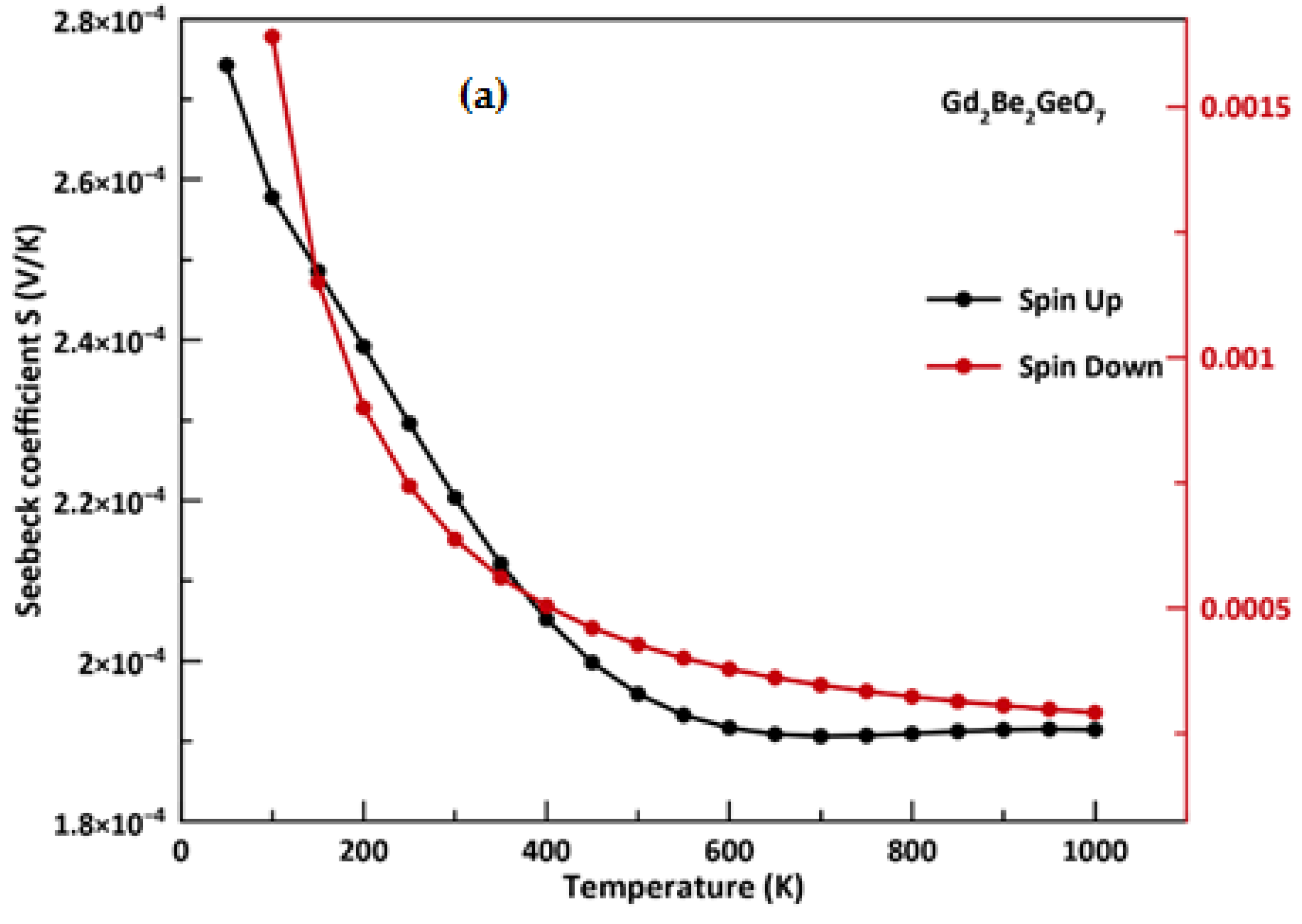
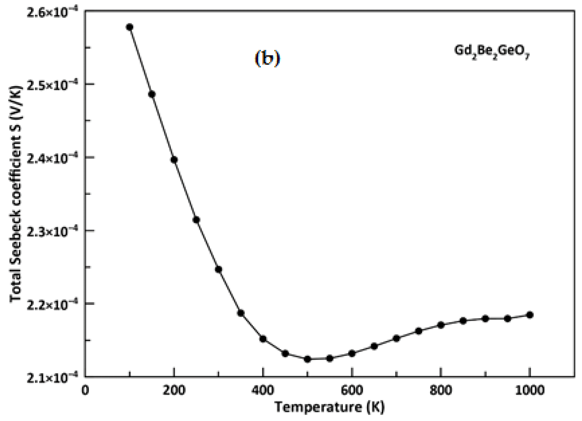
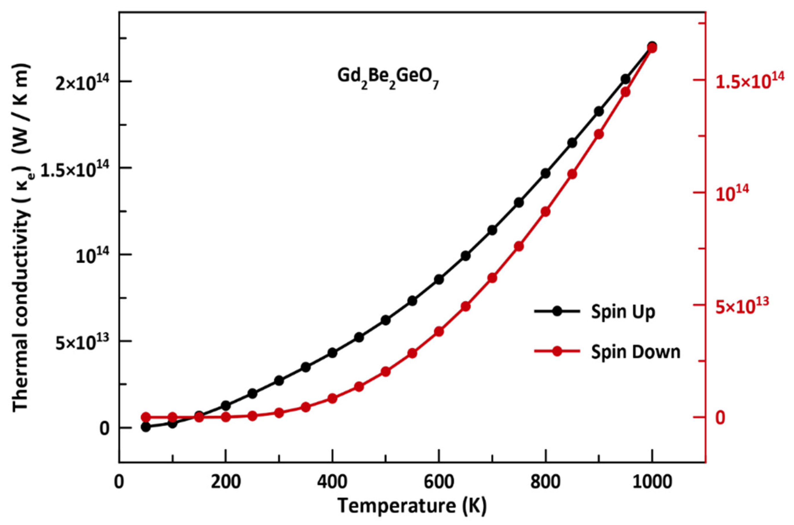
3.5. Thermoelectric Properties

In addition to detailed optoelectronic descriptions given obviously for the melilite-type Gd2Be2GeO7 compound, in this subsection, we extended our investigation to explore its thermoelectric properties in order to study its ability to convert waste heat into useful electricity. The efficiency of thermoelectric power generation, on the other hand, is assessed by a dimensionless parameter called figure of merit (ZT), which is given as ZT = S2σT/(κe + κL), where S is the Seebeck coefficient, T is the absolute temperature, and κee and κLL are the material’s electronic and lattice thermal conductivities, respectively [47,48,49,50,51,52,53]. We used the BoltzTraP code [30] with a mesh of 18 × 18 × 28 k-points for this purpose. Variation of the Seebeck coefficient as a function of temperature of intrinsic (pure) Gd2Be2GeO7 material is presented for the chemical potential μ = 0, which is in the middle of the band gap for spin-up and spin-down channels (see Figure 13a). The behavior of the Seebeck coefficient was relatively similar in the two spin channels, even though we stated different values, but the variation with temperature demonstrated a declining tendency in both spin-up and spin-down channels, respectively, from a very high value of ~270 μV/K and ~1700 μV/K. The Seebeck coefficients in both spin channels are positive, indicating that the holes are substantially dominating in this material.
Furthermore, we calculated the absolute Seebeck coefficient given by the following formula [47,48,49,50,51,52,53]:
S tot = σ ( ) S ( ) + σ ( ) S ( ) σ ( ) + σ ( )
The Seebeck coefficient is plotted as a function of temperature in Figure 13b, and it was positive throughout the temperature range for the examined compound, implying that holes are the charge carriers and that the spin-down state dominates the spin-up state. The presence of a low carrier concentration is indicated by the sharply higher values of the computed total S at lower temperatures <300 K. It has a value of 224.68 μV/K at room temperature, and we see a little drop in the total Seebeck value at higher temperatures. As a result, the computed Seebeck coefficients of Gd2Be2GeO7 compound in this study make it a promising material for thermoelectric devices.
To make a good thermoelectric device, the TE material used should have a high S, as well as high σ and low k = κe + κL at the same time [47,48,49,50,51,52,53]. The results of temperature dependence of the electronic thermal conductivity (κel(W/K⋅m)) for the two spin channels are shown in Figure 14 for the considered compound. We can clearly see that the κel after saturated values at low temperatures starts to increase rapidly with increasing temperature for the two spin channels (down and up). The κel values at room temperature are 1.984 × 10¹² W/K⋅m and 2.718 × 10¹³ W/K⋅m for spin-down and spin-up channels, respectively. One can state that the compound under discussion shows important thermal behavior near room temperature where the thermal conductivity has lower values and higher Seebeck coefficient as expected, as shown in Figure 13b and Figure 14.
The higher the ZT value, the higher the thermoelectric conversion efficiency. The variation of ZT with temperature is shown in Figure 15 for the compound under discussion for the spin channels. Our results show that reasonable performance associated with ZT values around 1 is probably likely for the minority spin channel, particularly at 100K. Furthermore, it can be clearly seen that the ZT value decreases gradually with increasing temperature, while, for the majority spin channel, ZT reaches a value of about 0.89 at low temperature and then starts to decrease with increasing temperature. Higher values of ZT (approximately 0.99 and 0.70) for a large temperature range indicate that the examined compound has good thermoelectric performance and could be a suitable material for thermoelectric generator applications. The mobility of free charge carriers causes an electrical conductivity (σ/τ) in transport properties, which is a key component that must be high for desired thermoelectric materials to lower the Joule heating effect [47,48,49,50,51,52,53,54]. Figure 16 shows the predicted electrical conductivity (σ/τ) of the Gd2Be2GeO7 compound as a function of temperature for both spins (up and down) configurations. The material exhibits approximately the same behavior in both channel configurations and σ/τ increases at given temperatures showing semiconductor behavior. Despite that, in the case of spin-down channel the value of σ/τ remains constant at low temperatures but above 300 K, a strong variation of σ/τ is observed with temperature.
The reported value of electrical conductivity at ambient temperature is 1.69 × 10¹⁸ (Ω m s)−1, which increases to 4.51 × 10¹⁸ (Ω m s)−1 around 1000 K in the spin-up channel. The value of the spin-down channel, on the other hand, climbs dramatically from 1.59 × 10¹⁶ (Ω m s)−1 at room temperature to 1.58 × 10¹⁸ (Ω m s)−1 at 1000 K. When compared to the spin-down arrangement, the electrical conductivity of the spin-up configuration is higher.

4. Conclusions

The structural, optoelectronics, and transport characteristics of the melilite-type Gd2Be2GeO7 compound have been investigated using the FP-LAPW method with the GGA-PBE and TB-mBJ functionals. From the obtained results, the important following conclusions can be drawn:
  • The calculated lattice constants agree well with the available experimental data.
  • The studied Gd2Be2GeO7 as thin film could be a good transparent in the visible spectrum (400–700 nm) for very thin thickness of 100 nm which makes it a suitable candidate for optical coating design devices; furthermore, it can be more efficient for applications in the ultraviolet (UV) region of the spectrum, and it could be useful for the high frequency UV device applications regarding the high absorbance peaks found in the range of 200 nm to 300 nm.
  • From spin-polarized thermoelectric calculations, the material under discussion presents adequate Seebeck coefficients around room temperature; furthermore, we found higher values of the figure of merit (around 0.99 and 0.70) over large temperature ranges which suggest that this material exhibits good thermoelectric performance and it could be a promising material for applications in thermoelectric generators.
  • Finally, the electrical conductivity (σ/τ) as a function of temperature exhibits the behavior of a typical semiconductor.

Author Contributions

Conceptualization, F.C., N.B., Y.A.K., H.K., R.M., R.K., A.B., M.B.K. and S.G.-S.; methodology, F.C., N.B. and Y.A.K.; software, F.C., N.B., Y.A.K., R.K., M.B.K. and S.G.-S.; validation, F.C., N.B., Y.A.K., H.K., R.M., R.K., A.B., M.B.K. and S.G.-S.; formal analysis, F.C., N.B., Y.A.K., H.K., R.M., R.K., A.B., M.B.K. and S.G.-S.; investigation, F.C., N.B., Y.A.K., H.K., R.M., R.K., A.B., M.B.K. and S.G.-S.; resources, F.C., N.B., Y.A.K., H.K., R.M., R.K., A.B., S.B.-O., M.B.K. and S.G.-S.; data curation, F.C., N.B., Y.A.K., H.K., R.M., R.K., A.B., M.B.K. and S.G.-S.; writing—original draft preparation, F.C., N.B., Y.A.K., H.K., R.M., R.K., A.B., M.B.K. and S.G.-S.; writing—review and editing, F.C., N.B., Y.A.K., H.K., R.M., R.K., A.B., M.B.K. and S.G.-S.; visualization, F.C., N.B. and Y.A.K.; supervision, F.C., N.B., Y.A.K. S.B.-O. and S.G.-S.. All authors have read and agreed to the published version of the manuscript.

Funding

This research received no external funding.

Institutional Review Board Statement

Not applicable.

Informed Consent Statement

Not applicable.

Data Availability Statement

The data used to support the findings of this study are available from the corresponding authors upon request.

Acknowledgments

The author F.C. acknowledge the financial Supporting Project number (B00L02UN220120220001), of the General Direction of Scientific Research and Technological Development (DGRSDT). The author S.B.-O. acknowledges Researchers Supporting Project number (RSP-2021/82), King Saud University, Riyadh, Saudi Arabia. Author S.G.-S. thanks Alfaisal University Research Office for supporting her research with internal research grant 22413.

Conflicts of Interest

The authors declare no conflict of interest.

References

  1. Nurse, R.W.; Midgley, H.G. The system CaO-fe2O3-al2O 3-sio2. J. Iron Steel Inst. 1953, 174, 121. [Google Scholar]
  2. Burzo, E. Melilites and related silicateS. In Sorosilicates; Springer: Berlin/Heidelberg, Germany, 2009; Volume 14, pp. 29–60. [Google Scholar]
  3. Louisnathan, S.J. Refinement of the crystal structure of a natural gehlenite, Ca2Al(Al, Si)2O7. Can. Mineral. 1971, 10, 822–837. [Google Scholar]
  4. Kuang, X.; Green, M.A.; Niu, H.; Zajdel, P.; Dickinson, C.; Claridge, J.B.; Jantsky, L.; Rosseinsky, M.J. Interstitial oxide ion conductivity in the layered tetrahedral network melilite structure. Nat. Mater. 2008, 7, 498–504. [Google Scholar] [CrossRef] [PubMed]
  5. Xia, Z.; Liu, Q. Progress in discovery and structural design of color conversion phosphors for LEDs. Prog. Mater. Sci. 2016, 84, 59–117. [Google Scholar] [CrossRef]
  6. Xia, Z.; Ma, C.; Molokeev, M.S.; Liu, Q.; Rickert, K.; Poeppelmeier, K.R. Chemical Unit Cosubstitution and Tuning of Photoluminescence in the Ca2(Al1–xMgx)(Al1–xSi1+x)O7:Eu2+ Phosphor. J. Am. Chem. Soc. 2015, 137, 12494–12497. [Google Scholar] [CrossRef]
  7. Louisnathan, S.J. Refinement of the crystal structure of hardystonite, Ca2ZnSi2O7. Z. Krist. Cryst. Mater. 1969, 130, 427. [Google Scholar] [CrossRef]
  8. Weiss, J.; Rosenstein, G. Addition of Ba2TiSi2O8 to manganese-doped barium titanate: Effect on oxygen diffusion and grain-boundary composition. J. Mater. Sci. 1988, 23, 3263–3271. [Google Scholar] [CrossRef]
  9. Peng, C.; Tsao, R.; Chou, Z. Gugiaite, Ca2BeSi2O7, a new beryllium mineral and its relation to the melilite group. Sci. Sin. 1962, 11, 977–988. [Google Scholar]
  10. Warren, B.E. The structure of melilite (Ca,Na)2(Mg,Al)1(Si,Al)2O7. Z. Kristallogr. 1930, 74, 131–138. [Google Scholar] [CrossRef]
  11. Ben Yahia, H.; Essehli, R.; Belharouak, I.; Gaudin, E. Crystal structure and magnetic properties of K2CoV2O7. Mater. Res. Bull. 2015, 71, 7–10. [Google Scholar] [CrossRef]
  12. Matsubara, S.; Miyawaki, R.; Kato, A.; Yokoyama, K.; Okamoto, A. Okayamalite, Ca2B2SiO7, a new mineral, boron analogue of gehlenite. Mineral. Mag. 1998, 62, 703–706. [Google Scholar] [CrossRef]
  13. Akasaka, M.; Ohashi, H. 57Fe mössbauer study of synthetic Fe3+-melilites. Phys. Chem. Miner. 1985, 12, 13–18. [Google Scholar] [CrossRef]
  14. Smith, J.V. Reexamination of the crystal structure of melilite. Amer. Miner. 1953, 38, 643–661. [Google Scholar]
  15. Smith, J.V. X-ray-emission microanalysis of rock-forming minerals. I. Experimental techniques. J. Geol. 1965, 73, 830–864. [Google Scholar] [CrossRef]
  16. Tyutyunnik, A.P.; Zubkov, V.G.; Surat, L.L.; Slobodin, B.V.; Svensson, G. Synthesis and crystal structure of the pyrovanadate Na2ZnV2O7. Powder Diffr. 2005, 20, 189–192. [Google Scholar] [CrossRef]
  17. Kloss, S.D.; Weidmann, N.; Niklaus, R.; Schnick, W. High-Pressure Synthesis of Melilite-type Rare-Earth Nitridophosphates RE2P3N7 and a Ba2Cu[Si2O7]-type Polymorph. Inorg. Chem. 2016, 55, 9400–9409. [Google Scholar] [CrossRef] [PubMed]
  18. Ochi, Y.; Morikawa, H.; Minato, I.; Marumo, F. Preparation and magnetic property of new rare earth compounds R2GeBe2O7 (R = La, Pr, Sm, Gd, Dy, Er) and Y2GeBe2O7. Mat. Res. Bull. 1982, 17, 911–916. [Google Scholar] [CrossRef]
  19. Ashtar, M.; Bai, Y.; Xu, L.; Wan, Z.; Wei, Z.; Liu, Y.; Marwat, M.A.; Tian, Z. Structure and Magnetic Properties of Melilite-Type Compounds RE2Be2GeO7 (RE = Pr, Nd, Gd–Yb) with Rare-Earth Ions on Shastry–Sutherland Lattice. Inorg. Chem. 2021, 60, 3626–3634. [Google Scholar] [CrossRef]
  20. Hohenberg, P.; Kohn, W. Inhomogeneous Electron Gas. Phys. Rev. 1964, 136, B864–B871. [Google Scholar] [CrossRef] [Green Version]
  21. Kohn, W.; Sham, L.J. Self-Consistent Equations Including Exchange and Correlation Effects. Phys. Rev. 1965, 140, A1133–A1138. [Google Scholar] [CrossRef] [Green Version]
  22. Andersen, O.K. Linear methods in band theory. Phys. Rev. B. 1975, 12, 3060–3083. [Google Scholar] [CrossRef] [Green Version]
  23. Singh, D.J. Plane Waves, Pseudopotentials and the LAPW Method; Kluwer Academic: Dodrecht, The Netherlands, 1994. [Google Scholar]
  24. Schwarz, K.; Blaha, P.; Madsen, G.K.; Kvasnicka, D.; Luitz, J. An Augmented Plane Waves + Local Orbital Program for calculating Crystal Properties; Institut Für Physikalische und Theoretische Chemie: Vienna, Austria, 2001. [Google Scholar]
  25. Perdew, J.P.; Burke, K.; Ernzerhof, M. Generalized Gradient Approximation Made Simple. Phys. Rev. Lett. 1996, 77, 3865. [Google Scholar] [CrossRef] [PubMed] [Green Version]
  26. Becke, A.D.; Johnson, E.R. A simple effective potential for exchange. J. Chem. Phys. 2006, 124, 221101. [Google Scholar] [CrossRef] [PubMed]
  27. Tran, F.; Blaha, P. Accurate Band Gaps of Semiconductors and Insulators with a Semilocal Exchange-Correlation Potential. Phys. Rev. Lett. 2009, 102, 226401. [Google Scholar] [CrossRef] [PubMed]
  28. Koller, D.; Tran, F.; Blaha, P. Merits and limits of the modified Becke-Johnson exchange potential. Phys. Rev. B 2011, 83, 195134. [Google Scholar] [CrossRef] [Green Version]
  29. Koller, D.; Tran, F.; Blaha, P. Improving the modified Becke-Johnson exchange potential. Phys. Rev. B 2012, 85, 155109. [Google Scholar] [CrossRef] [Green Version]
  30. Madsen, G.K.; Singh, D.J. BoltzTraP. A code for calculating band-structure dependent quantities. Comput. Phys. Commun. 2006, 175, 67–71. [Google Scholar] [CrossRef] [Green Version]
  31. Murnaghan, F.D. The Compressibility of Media under Extreme Pressures. Proc. Natl. Acad. Sci. USA 1944, 30, 244. [Google Scholar] [CrossRef] [Green Version]
  32. Birch, F. Finite Elastic Strain of Cubic Crystals. Phys. Rev. 1947, 71, 809. [Google Scholar] [CrossRef]
  33. Available online: https://materialsproject.org/materials/mp-650715?chemsys=Gd-Be-Ge-O (accessed on 17 August 2022).
  34. Ambrosch-Draxl, C.; Sofo, J.O. Linear optical properties of solids within the full-potential linearized augmented planewave method. Comput. Phys. Commun. 2006, 175, 1–14. [Google Scholar] [CrossRef] [Green Version]
  35. Amin, B.; Ahmad, I.; Maqbool, M.; Goumri-Said, S.; Ahmad, R. Ab initio study of the bandgap engineering of Al1−xGaxN for optoelectronic applications. J. Appl. Phys. 2011, 109, 023109. [Google Scholar] [CrossRef] [Green Version]
  36. Bassani, F.; Parravicini, G.P.; Ballinger, R.A.; Birman, J.L. Electronic States and Optical Transitions in Solids; Pergamon Press: Oxford, UK, 1973. [Google Scholar]
  37. Kramers, H.A. Collected Science Papers; North Holland: Amsterdam, The Netherlands, 1956. [Google Scholar]
  38. Kronig, R.D.L. On the Theory of Dispersion of X-Rays. J. Opt. Soc. Am. 1926, 12, 547. [Google Scholar] [CrossRef]
  39. Macleod, H.A. Thin Film Optical Filters, 2nd ed.; Adam Hilger: Bristol, UK, 1986. [Google Scholar]
  40. Born, M.; Wolf, E. Principles of Optics, 3rd ed.; Pergamon: Oxford, UK, 1965. [Google Scholar]
  41. Derkaoui, Z.; Kebbab, Z.; Miloua, R.; Benramdane, N. Theoretical study of optical characteristics of multilayer coatings ZnO/CdS/CdTe using first-principles calculations. Solid State Commun. 2009, 149, 1231–1235. [Google Scholar] [CrossRef]
  42. Miloua, R.; Kebbab, Z.; Chiker, F.; Sahraoui, K.; Khadraoui, M.; Benramdane, N. Determination of layer thickness and optical constants of thin films by using a modified pattern search method. Opt. Lett. 2012, 37, 449–451. [Google Scholar] [CrossRef] [PubMed]
  43. Miloua, R.; Kebbab, Z.; Chiker, F.; Khadraoui, M.; Sahraoui, K.; Bouzidi, A.; Medles, M.; Mathieu, C.; Benramdane, N. Peak, multi-peak and broadband absorption in graphene-based one-dimensional photonic crystal. Opt. Commun. 2014, 330, 135–139. [Google Scholar] [CrossRef]
  44. Boukabrine, F.; Chiker, F.; Miloua, R.; Kebbab, Z.; Khenata, R.; Prakash, D.; Bin Omran, S.; Verma, K. Combined theoretical studies of the optical characteristics of II-IV-V2 semiconductor thin films. Opt. Mater. 2016, 54, 200–206. [Google Scholar] [CrossRef]
  45. Lafort, A.; Kebaili, H.; Goumri-Said, S.; Deparis, O.; Cloots, R.; De Coninck, J.; Voué, M.; Mirabella, F.; Maseri, F.; Lucas, S. Optical properties of thermochromic VO2 thin films on stainless steel: Experimental and theoretical studies. Thin Solid Film. 2011, 519, 3283–3287. [Google Scholar] [CrossRef]
  46. Azam, S.; Khan, S.A.; Minar, J.; Goumri-Said, S. Exploring the electronic structure and optical properties of new inorganic luminescent materials Ba(Si,Al)5(O,N)8 compounds for light-emitting diodes devices. Curr. Appl. Phys. 2015, 15, 1160–1167. [Google Scholar] [CrossRef]
  47. Liu, M.-L.; Chen, I.-W.; Huang, F.-Q.; Chen, L.-D. Improved Thermoelectric Properties of Cu-Doped Quaternary Chalcogenides of Cu2CdSnSe4. Adv. Mater. 2009, 21, 3808–3812. [Google Scholar] [CrossRef]
  48. Fan, F.-J.; Yu, B.; Wang, Y.-X.; Zhu, Y.-L.; Liu, X.-J.; Yu, S.-H.; Ren, Z. Colloidal synthesis of Cu2CdSnSe4 nanocrystals and hot-pressing to enhance the thermoelectric figure-of-merit. J. Am. Chem. Soc. 2011, 133, 15910–15913. [Google Scholar] [CrossRef]
  49. Pei, Y.; Shi, X.; LaLonde, A.; Wang, H.; Chen, L.; Snyder, G.J. Convergence of electronic bands for high performance bulk thermoelectrics. Nature 2011, 473, 66. [Google Scholar] [CrossRef] [PubMed] [Green Version]
  50. Goumri-Said, S. Probing Optoelectronic and Thermoelectric Properties of Lead-Free Perovskite SnTiO3: HSE06 and Boltzmann Transport Calculations. Crystals 2022, 12, 1317. [Google Scholar] [CrossRef]
  51. Goumri-Said, S.; Alrebdi, T.A.; Deligoz, E.; Ozisik, H.; Kanoun, M.B. Revisiting the Electronic Structures and Phonon Properties of Thermoelectric Antimonide-Tellurides: Spin–Orbit Coupling Induced Gap Opening in ZrSbTe and HfSbTe. Crystals 2021, 11, 917. [Google Scholar] [CrossRef]
  52. Ding, G.; Gao, G.; Yao, K. High-efficient thermoelectric materials: The case of orthorhombic IV-VI compounds. Sci. Rep. 2015, 5, 9567. [Google Scholar] [CrossRef]
  53. Khan, W.; Azam, S.; Kanoun, M.B.; Goumri-Said, S. Optoelectronic structure and related transport properties of BiCuSeO-based oxychalcogenides: First principle calculations. Solid State Sci. 2016, 58, 86–93. [Google Scholar] [CrossRef]
  54. Azam, S.; Goumri-Said, S.; Khan, S.A.; Kanoun, M.B. Electronic, optical and thermoelectric properties of new metal-rich homological selenides with palladium–indium: Density functional theory and Boltzmann transport model. J. Phys. Chem. Solids 2020, 138, 109229. [Google Scholar] [CrossRef]
Figure 1. (a) The melilite crystalline structure of Gd2Be2GeO7 compound, (b) connectivity of GdO8 polyhedrons in the ab plane, and (c) c coordination environments of GdO8, BeO4, and GeO4 polyhedron.
Crystals 12 01397 g001
Figure 2. The total energy versus the volume for the ferromagnetic and non-magnetic Gd2Be2GeO7 compound.
Crystals 12 01397 g002
Figure 3. Brillouin zone of Tetragonal lattice. Path: Γ-X-M-Γ-Z-R-A-Z|X-R|M-A [33].
Crystals 12 01397 g003
Figure 4. The spin-polarized electronic band structure for Gd2Be2GeO7 compound in melilite tetragonal structure along with high symmetric directions with GGA-mBJ.
Crystals 12 01397 g004
Figure 5. The spin- polarized total and orbital projected density of states (DOS) for Gd2Be2GeO7 compound in melilite tetragonal structure using GGA + mBJ.
Crystals 12 01397 g005
Figure 6. The spin- polarized optical calculations using GGA + mBJ for Gd2Be2GeO7 compound.
Crystals 12 01397 g006
Figure 7. (a) The real part and (b) imaginary parts of the dielectric function in both parallel and perpendicular directions for Gd2Be2GeO7 compound.
Crystals 12 01397 g007
Figure 8. (a) Calculated refractive index n(ω)and (b) extinction coefficient k(ω)for Gd2Be2GeO7 compound in both parallel and perpendicular directions.
Crystals 12 01397 g008
Figure 9. For the Gd2Be2GeO7 compound, the absorption coefficientα(ω) was calculated in both parallel and perpendicular orientations.
Crystals 12 01397 g009
Figure 10. The transmittance spectra for Gd2Be2GeO7 thin films employing varying thicknesses in both processes of coating (free-standing layer and layer mounted on glasses).
Crystals 12 01397 g010
Figure 11. Absorbance spectra for Gd2Be2GeO7 thin films with various thicknesses in both coating processes (free-standing layer and layer supported on glasses).
Crystals 12 01397 g011
Figure 12. The reflectance spectra of Gd2Be2GeO7 thin films with various thicknesses in both coating processes (free-standing layer and layer supported on glasses).
Crystals 12 01397 g012
Figure 13. (a) Calculated total Seebeck coefficient (S) as a function of temperature for Gd2Be2GeO7 compound in both spin channels (up and down); (b) Calculated total Seebeck coefficient (S) as a function of temperature for Gd2Be2GeO7 compound.
Crystals 12 01397 g013aCrystals 12 01397 g013b
Figure 14. Calculated thermal conductivity κel/τ as a function of temperature in both spin channels (up and down) for Gd2Be2GeO7 compound.
Crystals 12 01397 g014
Figure 15. Figure of merit (ZT) for Gd2Be2GeO7 compound as a function of temperature in both spin channels (up and down).
Crystals 12 01397 g015
Figure 16. Variation of electrical conductivity (σ/τ) in both spin channels (up and down) as a function of temperature for Gd2Be2GeO7 compound.
Crystals 12 01397 g016
Table 1. Lattice constants a and c, bulk modulus B0, and its pressure derivative B’ parameters optimization in both ferromagnetic (FM) and nonmagnetic orders (NM). For comparison, experimental and other theoretical values are included [18,19].
Gd2Be2GeO7a ( Å )c ( Å )V ( Å )B0 (GPa)B’E0 (×106 eV)Reference
7.5164.878275.654160.953.880−1.371788Present workNM
7.5254.883276.567165.914.274−1.371821Present workFM
7.4804.842270.910---[18]
7.4944.842271.894---[19]
Table 2. The HVB and the LCB electron energies in eV (in the present work), evaluated with the GGA + mBJ exchange potential according to the majority spin (spin-up) and minority spin (spin-down) panels at different high-symmetry k-points for the Gd2Be2GeO7 compound.
k-PointsMajority Spin (Spin-up)Minority Spin (Spin-down)
HVBLCBHVBLCB
Γ−0.1996.327−0.1833.792
X−0.1327.154−0.2463.792
M−0.0877.283−0.2123.796
Z0.0076.862−0.1393.788
R−0.0447.025−0.1913.79
A−0.087.026−0.1643.803
Table 3. Calculated magnetic moments of each atom, interstitial, and cell for Gd2Be2GeO7 compound in μB unit compared to experimental data.
Gd2Be2GeO7μIntersμGdμBeμGeμO1μO2μO3μTotB)
0.6616.7290.0000.0010.0490.0180.0397.49 Present work
7.94– 7.20 [18]
7.05 [19]
Publisher’s Note: MDPI stays neutral with regard to jurisdictional claims in published maps and institutional affiliations.

