Abstract
A new generation of high-efficiency power devices is being developed using wide bandgap (WBG) semiconductors, like GaN and SiC, which are emerging as attractive alternatives to silicon. The recent interest in GaN has been piqued by its excellent material characteristics, including its high critical electric field, high saturation velocity, high electron mobility, and outstanding thermal stability. Therefore, the superior performance is represented by GaN-based high electron mobility transistor (HEMT) devices. They can perform at higher currents, voltages, temperatures, and frequencies, making them suitable devices for the next generation of high-efficiency power converter applications, including electric vehicles, phone chargers, renewable energy, and data centers. Thus, this review article will provide a basic overview of the various technological and scientific elements of the current GaN HEMTs technology. First, the present advancements in the GaN market and its primary application areas are briefly summarized. After that, the GaN is compared with other devices, and the GaN HEMT device’s operational material properties with different heterostructures are discussed. Then, the normally-off GaN HEMT technology with their different types are considered, especially on the recessed gate metal insulator semiconductor high electron mobility transistor (MISHEMT) and p-GaN. Hereafter, this review also discusses the reliability concerns of the GaN HEMT which are caused by trap effects like a drain, gate lag, and current collapse with numerous types of degradation. Eventually, the breakdown voltage of the GaN HEMT with some challenges has been studied.
Keywords:
GaN HEMT; normally off; reliability; challenges; power devices; semiconductor devices; wide bandgap 1. Introduction
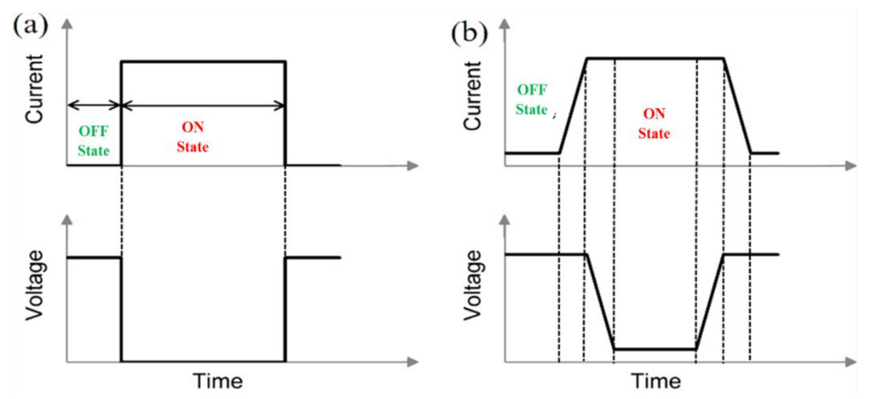
Electrical power has been a fundamental driver of humanity’s progress and is indispensable in our daily life. Power electronics are critical components of electrical power usage because they control, convert, and manage electric currents, voltages, or powers. They are extensively utilized in consumer items, energy harvesting, and usage, such as switching power supplies, power converters, power inverters, motor drives, etc. Figure 1 shows the different fields of operation of power devices with the required voltage and current ratings [1,2]. As depicted in Figure 2, a typical power electronic system includes a power source, a filtering mechanism, a power conditioner, a load, and a control circuit. A power conditioner is composed of a series of semiconductor devices working in a switched mode, in which the devices are turned between the “OFF” and “ON” states under the direction of the gate driver [1]. When turned “off”, an ideal switch should have no leakage current and a full voltage drop across it. If switched “on”, it should have a zero voltage drop across it (Figure 3). In actuality, the power devices exhibit a resistance during the on-state (RON) and a leakage current during the off-state. Under the common biasing conditions, the voltage across it is restricted by the off-state drain to source the breakdown voltage (BVDSS). Thus, to maximize the energy efficiency and minimize conversion losses, the most crucial properties of power devices to accomplish are a low RON and a high BVDSS.
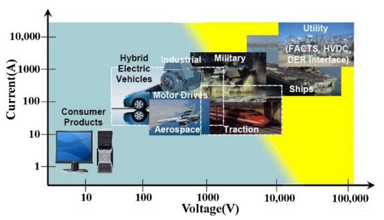
Figure 1.
Applications of power electronics in power management and control. Reproduced with permission [2]. Copyright 2019, the author(s). Published by Elsevier.
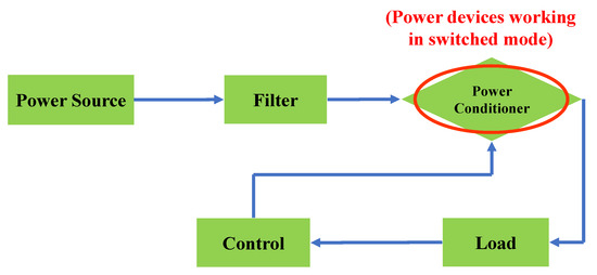
Figure 2.
Components of a power electronic system and power semiconductor devices in power conditioners.
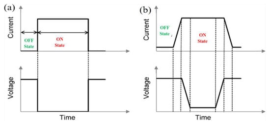
Figure 3.
The current and voltage across (a) an ideal power switching device and (b) a power switching device.
Moreover, Gallium Nitride (GaN) has risen as an attractive material for fabricating semiconductor devices over the last decade. Its excellent performance characteristics, like its wide band gap, high electron mobility, high breakdown field, low noise, high saturation velocity, and low thermal impedance, are essential for modern power device technology [3].
This review article will provide a basic overview of the various technological and scientific elements of the current GaN HEMT technology, where we summarize the recent and future potential market strategy of GaN HEMT power devices. Additionally, the previous and present data of the most extensively used commercially device, the normally-off GaN HEMT, are amalgamated, focusing explicitly on the insulator’s role in the recessed MISHEMT region and the metal on the p-GaN performances, which makes this review article more comprehensive compared to other review articles. Moreover, this review also discusses the reliability concerns of the GaN HEMT which are caused by trap effects like a drain, gate lag, and current collapse with numerous types of degradation.
1.1. Market Strategy of GaN HEMT Power Devices
GaN-based devices are being reported in various market-driven sectors, including RF power devices, photonics, high-frequency communications, control, and high-power conversion, which assists commerce’s and corporations in meeting the constantly expanding need for more outstanding metrics. The inherent robustness of the device enables it to compete effectively in the current markets for tiny, rugged, and highly dependable electronics, such as in vehicle, military, and space applications. GaN engineering appears promising for achieving the critical performance requirements and the possibility of sustained economic benefits upon its maturity.
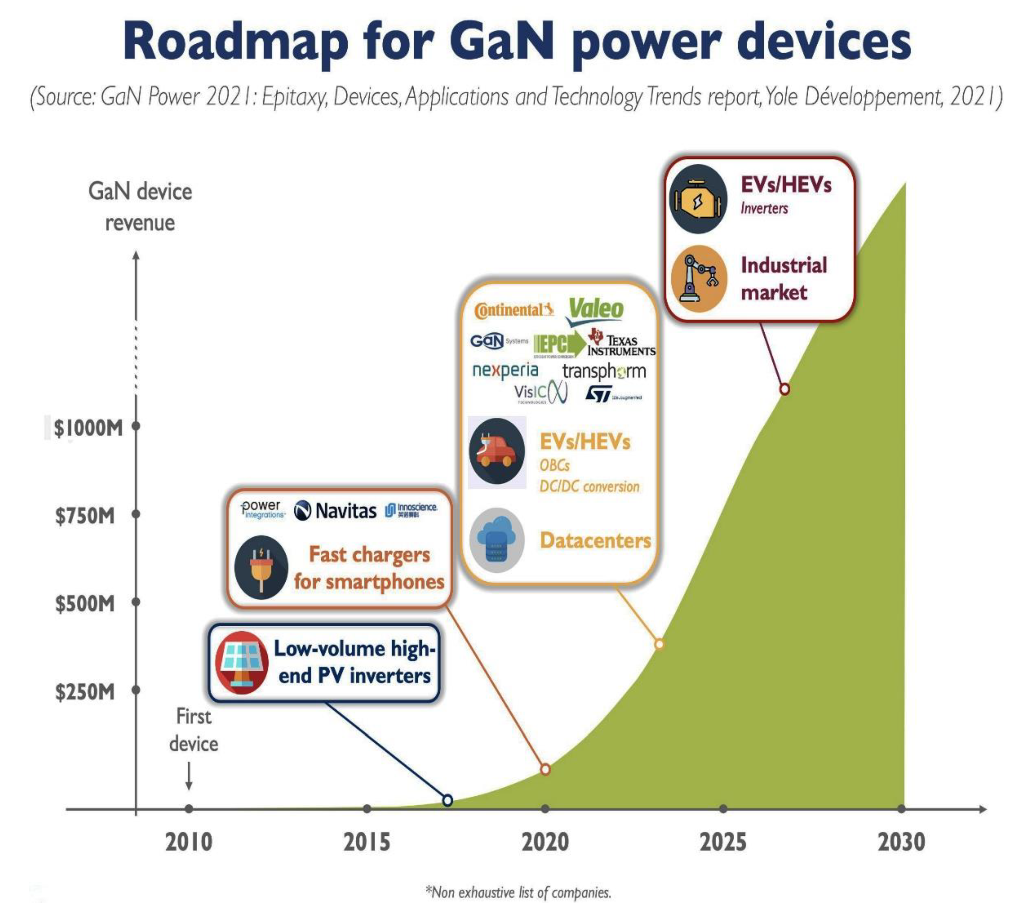
Figure 4 and Figure 5 show that according to Yole Développement (Yole), the power GaN market will double by 2020, surpassing the USD one billion mark in 2026. As an additional validation of this remarkable GaN market development, Yole projects that the telecom and datacom and automotive sectors will contribute to the total growth in the mid- to long-term, owing to GaNs rise in fast chargers. In the consumer market, GaN had a good year in 2020, owing to the technology adoption by various businesses, including Xiaomi, Lenovo, Samsung, Realme, Dell, LG, and other Chinese aftermarket firms. Yole anticipates that the GaN consumer power supply industry will be the primary driver, growing from USD 29 million in 2020 to about USD 672 million in 2026 at a compound annual growth rate (CAGR) of 69%. In the telecom and datacom sectors, where more efficient, smaller power supplies must comply with the stricter energy consumption standards, data centers and telecom operators are already interested in GaN devices.
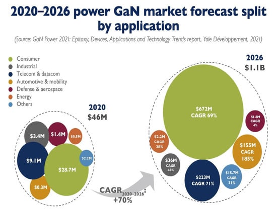
Figure 4.
GaN power market forecast split by application prediction by Yole. Reproduced with permission [4]. Copyright 2021, published by Yole Développement.
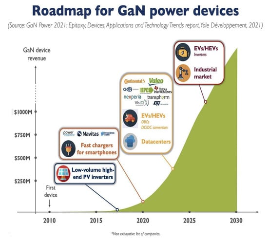
Figure 5.
Roadmap for GaN power devices prediction by Yole. Reproduced with permission [4]. Copyright 2021, published by Yole Développement.
Following Eltek, Delta, and BelPower’s recent small volume adoption of the GaN-based power supply, it was predicted that there would be a more significant market for GaN in 2020, with a market value of USD 9.1 million and a CAGR of 71% from 2020 to 2026, reaching more than USD 223 million in 2026. The automotive and mobility markets are also paying close attention to GaN because of significant incentives for vehicle electrification and a need to increase the driving range via A system efficiency improvement. AEC-qualified manufacturers include EPC, Transphorm, GaN Systems, and Texas Instruments. STMicroelectronics, a major IDM, also pursues GaN for EVs via partnerships and acquisitions. In 2022, GaN will likely infiltrate at limited levels, primarily via OEM and Tier-1 samples. Yole anticipates that the automobile and mobility industry will exceed a value of USD 155 million in 2026 [4].
While GaN continues to gain traction in the general consumer market, telecom, datacom, automotive, and mobility businesses will benefit from the “economy of scale impact” and price erosion. Indeed, Yole anticipates that a GaN adoption will increase in these areas, where reliability and affordability are critical, beginning in 2023–2024. In the long run, after GaN has shown its durability and high current capability at a lower price, it may be able to reach the more difficult EV/HEV inverter market and the conservative industrial industry, creating an extraordinary high-volume potential for GaN. Indeed, Nexperia and VisIC are developing GaN-based xEV inverter systems to compete with SiC and Si. Furthermore, as various industry experts previously said, GaN is more suitable for low-to-medium voltage applications (200–600 V), including a sizable share of the consumer electronic market (e.g., phone chargers, audio amplifiers, and computer power supplies). GaN is the most excellent contender to replace conventional Si devices in this voltage range. The 600–900 V voltage range is strategically important since it includes converters for electric cars (EVs), hybrid EVs, and inverters for sustainable energy (e.g., photovoltaic). GaN devices are projected to compete or coexist alongside SiC devices in this voltage range. Recent industry analyst studies [5] show that the GaN power device market is expected to grow dramatically, surpassing a value of USD 700 million in 2025, as illustrated in Figure 6.
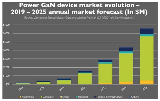
Figure 6.
GaN Power device market size prediction by Yole. Reproduced with permission [5]. Copyright 2020, published by Yole Développement.
1.2. Market Strategy of GaN HEMT RF Devices
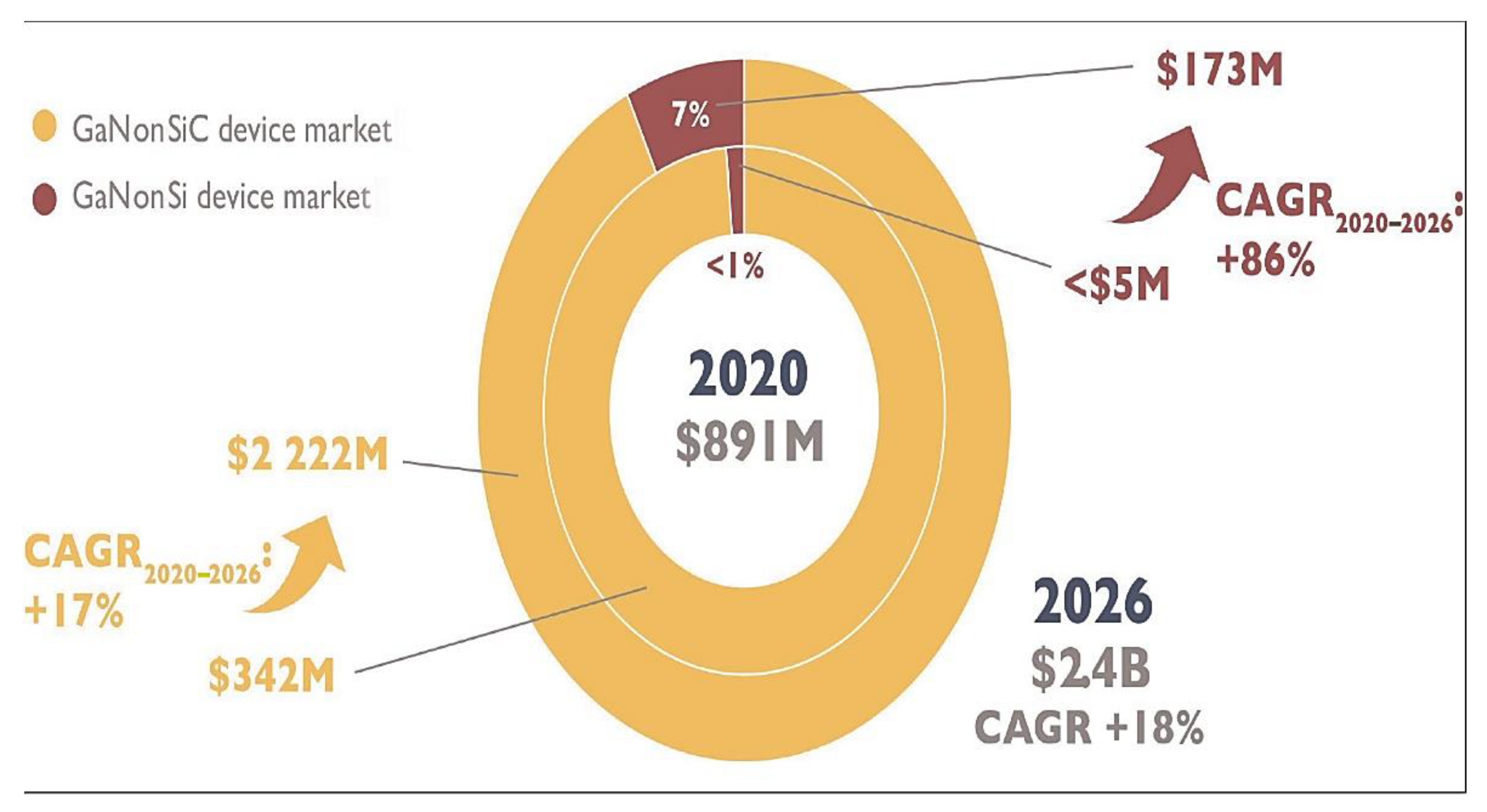
The gallium nitride (GaN) radio-frequency (RF) device market is rising at a compound annual growth rate (CAGR) of 18% from a USD 891 million value in 2020 to a more than USD 2.4 billion value by 2026, forecasts the market analyst firm Yole Développement [6]. It has been forecasted that the market will be dominated by defense and 5G telecom infrastructure applications, representing 49% and 41% of the entire market by 2026, respectively. In particular, the GaN-based macro/micro-cell sector will represent more than 95% of the GaN telecom infrastructure market in 2026, as reflected in Figure 7.

Figure 7.
GaN Power RF market evaluation by Yole. Reproduced with permission [6]. Copyright 2021, published by Yole Développement.
In the RF GaN industry, everything started with GaN-on-SiC (gallium nitride on silicon carbide) technology. Launched more than 20 years ago, GaN-on-SiC is now a serious rival to silicon LDMOS and gallium arsenide (GaAs) in RF power applications. Dominated by GaN-on-SiC technology, a vertical supply chain integration has been preferred in defense and 5G telecom applications. Therefore, GaN-on-SiC technology is still preferred in terms of its high-power density and thermal conductivity. In addition to its deep penetration in the military radar, GaN-on-SiC has also been the choice of telecom OEMs such as Huawei, Nokia, and Samsung for 5G massive MIMO infrastructures. Due to their high bandwidth and efficiency, GaN-on-SiC devices continuously take a share from LDMOS of the 5G market and are starting to benefit from the 6” wafer platform transition. In this context, the GaN-on-SiC device market is growing at a 17% CAGR from USD 342 million in 2020 to USD 2.222 billion in 2026. However, as a key challenger, GaN-on-Si is still in the game, promising cost-efficient and scalable solutions. The recent entry of foundries and synergy with the emerging power electronics GaN-on-Si industry can also help GaN-on-Si RF to gain momentum in the longer term, says Yole. Driven by handsets but also defense and 5G telecom infrastructure applications, the GaN-on-Si device market is growing at a CAGR of 86% from less than USD 5 million in 2020 to USD 173 million in 2026 [6], as illustrated in Figure 8.
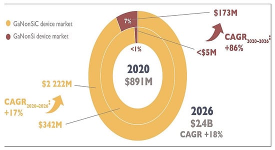
Figure 8.
GaN RF application breakdown by substrate markets as compiled in 2021 by Yole. Reproduced with permission [6]. Copyright 2021, published by Yole Développement.
2. Wide Bandgap Semiconductors for Power Devices
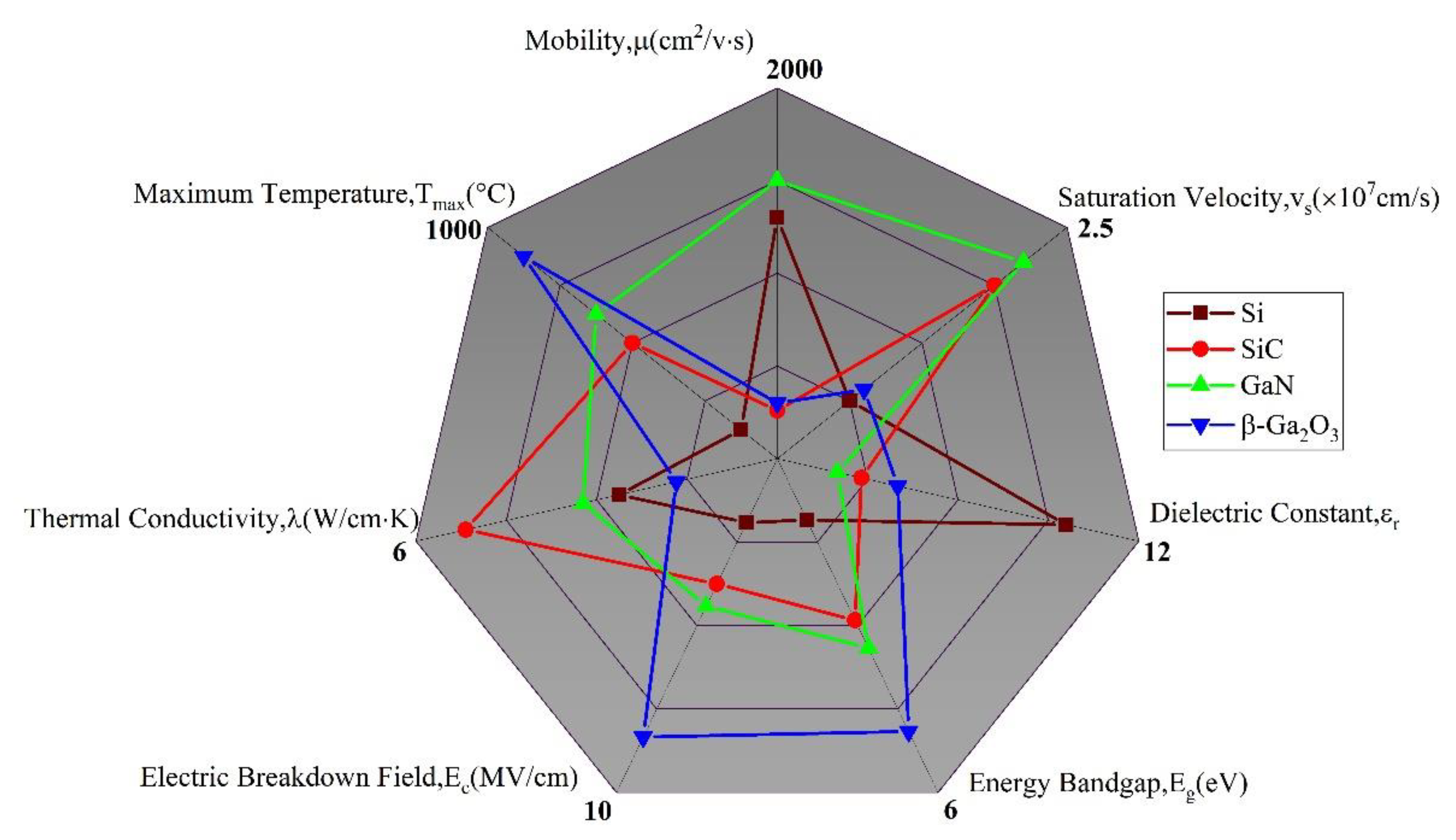
Due to the many constraints of silicon-based power devices and the rising interest in increasing performances, new semiconductor materials for next-generation power electronic devices are being developed. Because of their better electrical properties, wide bandgap (WBG) semiconductors like GaN, β-Ga2O3, and SiC have emerged as market leaders in power electronic applications. Since the material’s small bandgap is responsible for many of the constraints for Si-based devices, wide bandgap power devices have a better performance with a larger blocking voltage, dependability, and efficiency with less thermal constraint [7,8,9]. Thus, GaN, β-Ga2O3, and SiC have a bandgap which is two to four times that of Silicon. A bigger energy bandgap makes it more challenging to break the bonding and generate free charge carriers for a current conduction, which results in a less conductive material and transistors with lower leakage currents and a more excellent stability at high temperatures. On the contrary, β-Ga2O3 devices have a substantially greater breakdown voltage compared to Si devices when their on-resistances are comparable. Moreover, GaN devices have a larger saturation on-current than Si devices due to the higher saturated electron velocity of GaN. Additionally, the carrier drift velocity directly connects with the switching speed of semiconductor devices, and this device has a quicker recovery time and a lower reverse recovery current. On the other hand, SiC presents a thermal conductivity three times higher than Si and GaN and 16 times higher than β-Ga2O3. The characteristics of Si are compared to those of WBG semiconductors such as SiC, β-Ga2O3, and GaN in Figure 9 [10,11,12].

Figure 9.
Comparison of wide bandgap materials with Si.
However, numerous figures of merit (FOM) have been proposed to compare the merit of several semiconductor materials for a provided application. A higher figure of merit number indicates a better performance. Hence, Johnson’s figure of merit (JFOM) provides an indication of the material suitability for high-power applications at high frequencies, which can be estimated by using Equation (1) [13]:
Here, denotes the saturation electron velocity, and Ec denotes the critical electric field. On the contrary, to analyze the optimum results of field effect transistors in low-frequency power switching applications, Baliga’s figure of merit (BFOM) was devised where conductive loss predominates, as shown in Equation (2) [14]:
Here, εr denotes the semiconductor’s dielectric constant, and µ denotes the electron mobility. For a high frequency, the Baliga high-frequency FOM (BHFOM) in Equation (3) evaluates the devices where the switching losses are the most significant [14]:
Here, the gate drive voltage is Vg, while the breakdown voltage is VBR. By using the device’s on-state specific resistance, , and the critical electric field, Ec, the latter is coupled to an experimental figure of merit on Equation (4). Eventually, to account for the high power, high temperature, and high-frequency performance simultaneously, the combined FOM (CFOM) was devised, as shown in Equation (5) [15]:
Table 1 shows the multiple figures of merit for the β-Ga2O3 potential high-frequency and high-power performance compared to other competing semiconductor materials. According to this table, β-Ga2O3 is a great contender for high-frequency power applications. In JFOM, the β-Ga2O3 is more remarkable than approximately 1.5 times that of GaN, 10 times that of SiC, and about a thousand times that of Si. Consequently, β-Ga2O3 outperforms Si, GaN, and SiC in terms of its high-frequency/high-power performance. Similarly, in BFOM, β-Ga2O3 is more remarkable than around four times that of GaN, ten times that of SiC, and a thousand times that of Si [16]. Moreover, wide-bandgap semiconductors, regardless of their FOM, provide better performance features for high-power, high-frequency applications. Thus, due to the high values of the Baliga FOM and the breakdown field, β-Ga2O3 is a promising candidate for the next generation of high-power devices, including HEMT, Schottky barrier diodes (SBDs), and field-effect transistors (FETs).

Table 1.
Figures of merit of GaN and competing semiconductor materials in power electronics [12].
2.1. Lattice Structure and Polarization of GaN-Based Semiconductors
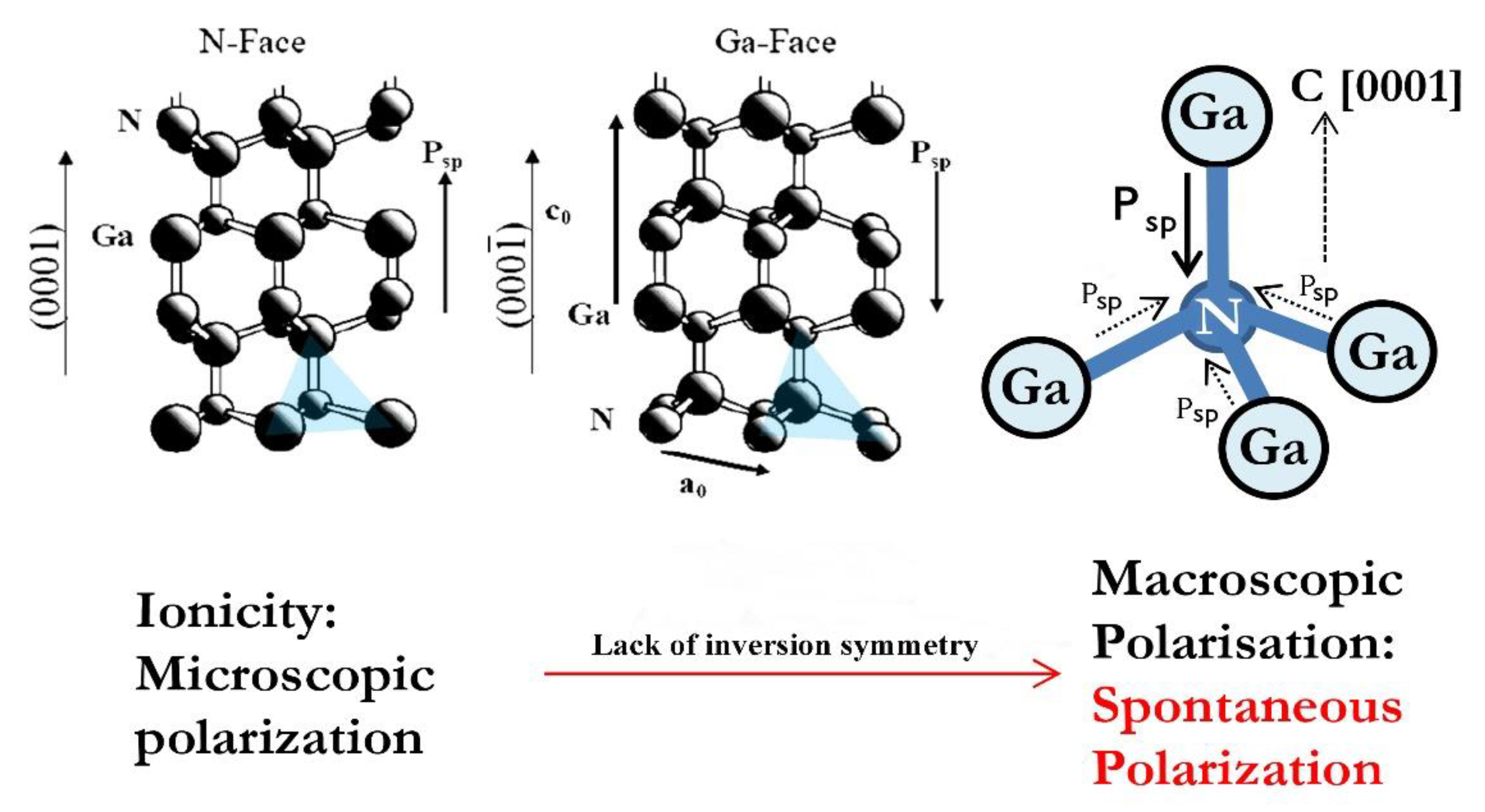
Wurtzite hexagonal close-packed (HCP) (α-phase), rock-salt, and cubic zincblende (β-phase) are examples of III-N-based semiconductors, mainly GaN-based semiconductors [17,18]. Figure 10 depicts the wurtzite crystal structure, which is particularly important for electronics and optoelectronics applications today. The hexagonal unit cell of wurtzite comprises two intersecting hexagonal close packed (HCP) sub-lattices. As illustrated in Figure 10, it is defined by two lattice parameters, the height of the cell c0, and the length of a side of the hexagonal base a0, in an ideal ratio Each sub-lattice is made up of one kind of atom. In relation to one another, the internal cell parameter u0 = 3/8 moves them along the c-axis. Table 2 presents the structural and polarization properties of III-Ns.

Figure 10.
The alignment of PSP and the tetrahedral bond structure of Ga-face and N-face heterostructures. Reproduced with permission [20]. Copyright 2019, Elsevier.

Table 2.
Structural and polarization parameters of III-N wurtzite semiconductors [17].
These ideal values are absent in the typical nitride compounds GaN, InN, and AlN and their associated alloys. The c0/a0 ratio deviates from the ideal lattice’s 1.633 as the non-ideality of the lattice grows [19].
Because of the very high electronegativity of the N atom, which is 3.04 on Pauling’s scale, and for Aluminum (1.61), Gallium (1.81), and Indium (1.78) atoms [19], consequently, the data for u0 and c0/a0 deviate from the optimum values given earlier [21]. Group III-N semiconductors have a particularly high polarization due to the crystal structure’s intrinsic electronic charge redistribution, which means a spontaneous polarization, Psp, [19]. The directions <0001> and <000> are not comparable due to a lack of inversion symmetry shown along its c-axis in the wurtzite structure. Hence, cation-face, i.e., Ga-face and anion-face, i.e., N-face, are the alternative polarities of GaN. The polarization field points change their position in the cation-face, i.e., Ga-face, surface towards the substrate. On the contrary, the polarization field points move in the opposite direction in the anion-face, i.e., N-face.
Because of the lack of this inversion symmetry, when the group III-N semiconductors’ lattice is imposed by stress in the <0001> direction, the ideal lattice values of the crystal structure’s c0 and a0 will shift to adapt to the stress. As a result, the strength of the polarization would shift. In the strained group III-N crystals, this extra polarization is known as piezoelectric polarization, Ppz [22]. For instance, the in-plane constant of the lattice a0 would drop, and the vertical constant of the lattice c0 would rise if the crystal of the nitride is subjected towards a biaxial compressive stress. Due to the piezoelectric and spontaneous polarizations working in opposing directions, the ratio of c0/a0 will climb to 1.633 of the perfect lattices, and the overall polarization strength will be reduced in the crystal. Moreover, when the tensile stress is imposed on the crystal, the spontaneous and piezoelectric polarization work simultaneously. As a result, the total polarization will rise. The piezoelectric coefficients e33 and e13 are evaluated for the piezoelectric polarization, Ppz [23,24], as shown in Equation (6),
Here, a0 and c0 are the lattice parameter equilibrium values, ε3 = (c − c0)/c0 is the strain along the c axis, and ε1 = ε2 = (a − a0)/a0 is the isotropic in-plane strain. The various strains in the lattice are connected in Equation (7). The elastic constants denoted by and . Combining Equations (1) and (2) provides the corresponding formula in Equation (8):
The equation will be negative if e33, c13, and c33 are positive, and the piezoelectric coefficient e13 is negative in wurtzite III-nitrides [25]. Thus, it is claimed that piezoelectric and spontaneous polarization are parallel under tensile stress layers, but they are anti-parallel under compressive stress layers. Polarization and gradients induce fixed sheet charges at the surfaces and interfaces of the AlGaN/GaN heterostructures. As a result, there are high electric fields within the heterostructure. The electric field in nitrides may approach 3 × 10⁶ V/cm, which enhances the hole or electron formation at the AlGaN/GaN contacts. This is called polarization-induced doping, which is the root of the two-dimensional electrons gas (2DEG) (discussed more in the below segment).
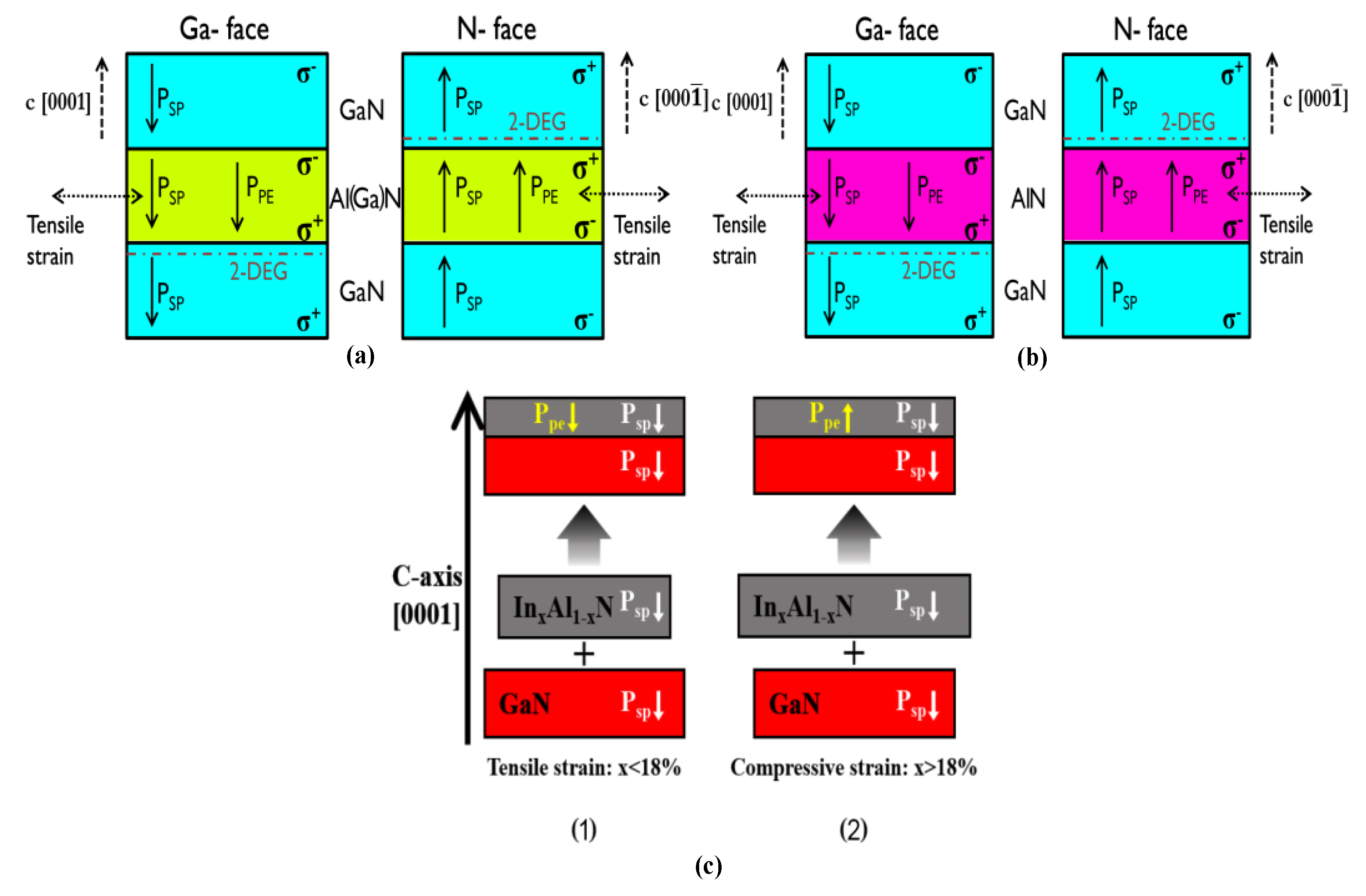
Figure 11a shows that growing a tiny epi AlGaN layer on top of a thicker GaN layer generates an AlGaN/GaN heterostructure. A 2DEG is generated at the interface between the AlGaN barrier and the GaN channel because of the Psp and Ppz, which may be a conduction channel consisting of exceptionally high mobility electrons even without any n-type doping, which is ideal for transistors. Both GaN and AlGaN have a significant Psp. When the material is strained, a Ppz component develops in GaN, AlN, or AlGaN. The piezoelectric polarization arises in the thin layer of AlGaN because it is beneath the tensile strain. In contrast, the layer of GaN is considerably thicker and nearly relaxed in an AlGaN/GaN heterostructure. Psp and Ppz are parallel when the AlGaN layer is under a tensile strain (Figure 11a) [23]. So, to acquire the AlGaN characteristics and determine the actual polarization-induced charge densities, we apply Equations (9) through to (14) [26].

Figure 11.
Polarization charges in an (a) AlGaN/GaN, (b) AlN/GaN, and (c) InAlN/GaN heterostructure. Reproduced with permission [20]. Copyright 2019, Elsevier.
Similarly, 2DEG is generated at the interface between the AlN barrier and the GaN channel for the reason of the Psp and Ppz, as illustrated in Figure 11b. However, due to the large difference in the spontaneous and piezoelectric polarizations between the GaN and AlN layers, the 2DEG, which forms near the AlN/GaN interface, can reach over 3 × 1013 cm−2 for an extremely thin AlN barrier layer thickness (d < 5 nm), along with a high mobility (>1000 cm2/V·s) and a very low sheet resistance (Rsh < 150 Ω/□) [27]. On the contrary, due to the high aluminum content and the associated degree of bond polarity, a spontaneous polarization in in the In0.18Al0.82N/GaN heterostructures generates two-dimensional electrons gas (2DEG) densities which are competitive with AlGaN/GaN structures without the need for a strain-induced piezoelectric component. For InAlN alloys, the strain state can go from tensile when the In % is lower than ~18%, to compressive when the In % is higher than ~18%, as shown in Figure 11c ((1), (2)), respectively; when the InAlN is the lattice matched to the GaN buffer, the In % is around 18%. Moreover, the implementation of the InAlN barriers with the In % around 18% allows for the strain to be controlled in the InAlN/GaN heterostructure, and a lattice-matched In0.18Al0.82N layer to the GaN sheet charge density is almost three times higher than for the conventionally grown Al0.25Ga0.75N barriers on the GaN channels [28].
Spontaneous polarization can be observed in Equation (9). As an alternative, for a precise interpolation, a bowing parameter b might be utilized in Equation (10) [29]. The constants of the lattice for AlxGa1-xN are in Equations (11) and (12) where x = Al mole fraction. The elastic constants are presented in Equations (13) and (14).
The above equations indicate that if the Al content in the AlGaN layer rises, the overall polarization will soar. A polarization charge density (ρp) corresponds to a polarization gradient (P) in space (ρp = ∇P). Therefore, at the AlGaN/GaN abrupt contact, a fixed polarization charge would be induced. In the case of AlGaN/GaN, fixed positive induced polarization charges form at the interface. Even without n-type doping, the positive polarization-induced charges at the interface of AlGaN/GaN attract the free electrons. Because of this, in the AlGaN/GaN interface, 2DEG is generated. The carrier density of 2DEG may also be estimated analytically by using polarization [30].
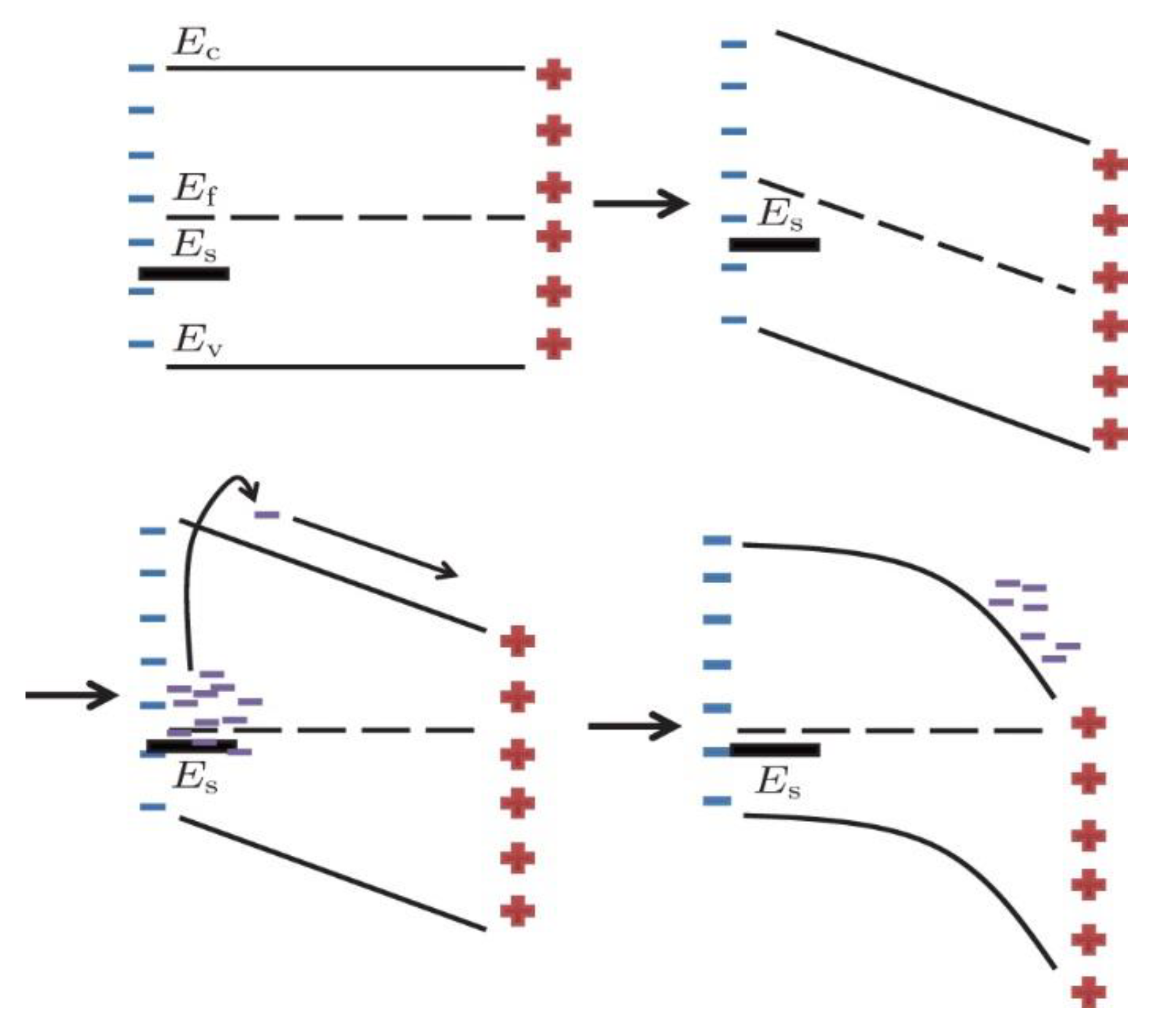
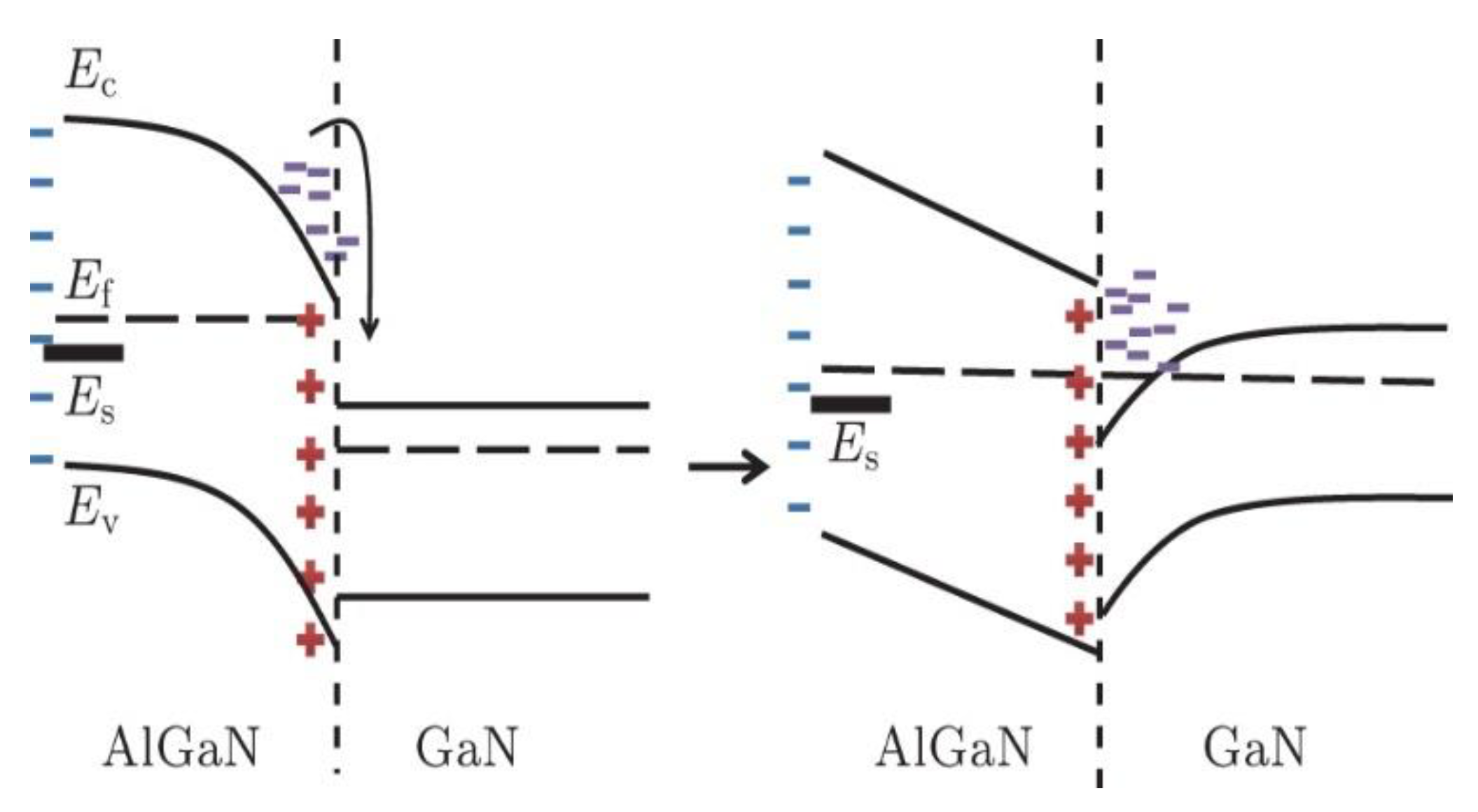
The 2DEG creation is explained in a few Figures. Thus, in the undoped AlGaN/GaN heterojunction, the 2DEG creation may be described on the AlGaN surface by introducing donor states. An the isolated AlGaN material energy band gap is depicted in Figure 12 with the presence of surface donor states. The isolated AlGaN material is believed to be free of compressive/tensile forces. The Fermi level is attained if the density of the AlGaN material is enough. So, the electrons are advanced to the conduction band and drawn to the other side by polarization-induced electric fields after the Fermi level exceeds the donor state-level ES. The Fermi level causes the dropping of the electrons into the GaN side when the AlGaN and GaN materials come into contact. The 2DEG results from a buildup of electrons at the interface, as displayed in Figure 13. Thus, combined with the ionized surface donor, it produces an electric field that points between the interface and the surface in the AlGaN layer to minimize the polarization field [31].
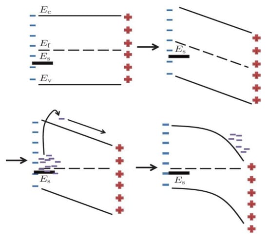
Figure 12.
An undoped AlGaN material with ES surface donor states has an energy band. Electrons are advanced into the conduction band and gravitate toward the electric field created by positive polarization. Reproduced with permission from Chin. Phys. B. [31].
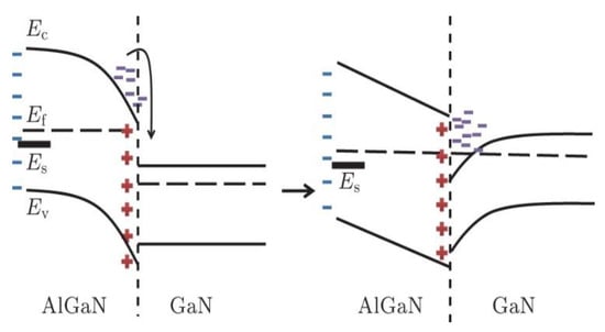
Figure 13.
In the 2DEG quantum well, the buildup of electrons is shown in the energy band of an undoped AlGaN/GaN heterojunction. Reproduced with permission from Chin. Phys. B. [31].
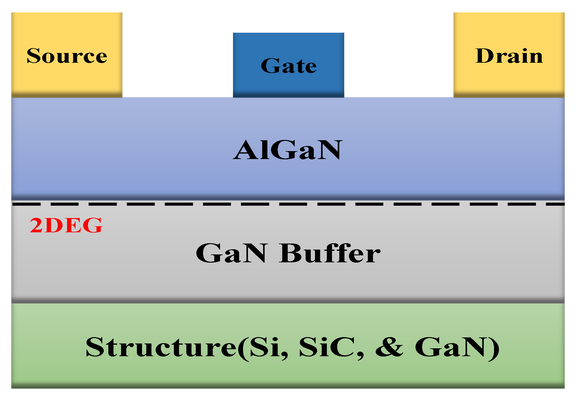
As noted previously, the creation of 2DEG occurs naturally at the interface when a tiny strained AlGaN layer is developed on top of a thicker relaxed GaN layer. Due to the confinement of high mobility electrons, this 2DEG exhibits very conductively in the quantum well. Because of the reduced surface scattering, the electron mobility rises between the unstrained GaN and 2DEG areas at roughly 1000 cm2/V·s and 1500–2000 cm2/V·s, respectively. For HEMTs, a transistor channel with a higher mobility and electron concentration seems appropriate. Figure 14 depicts a basic AlGaN/GaN HEMT design. The substrates are mostly SiC, silicon, sapphire, or GaN, and a buffer layer is formed to relieve the strain induced by a foreign substrate’s lattice mismatch. The 2DEG creates a native channel between the source and drain of the device.. In most early AlGaN/GaN transistors, a Schottky gate electrode is formed by the deposition of Ni/Au or Pt metal on top of the AlGaN layer [32]. The GaN HEMT, with the 2DEG present at the interface of the AlGaN/GaN, was first shown in early 1993 [33]. The channel is regulated by supplying a gate voltage (VGS) and, therefore, a vertical electrical field to deplete or augment the channel, making it less conductive in the off-state or more conductive in the on-state. Later, researchers from all over the globe have progressively reported high-performance GaN HEMTs for high-power and RF applications [34,35].
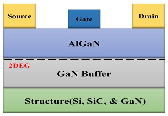
Figure 14.
AlGaN/GaN HEMT layout and 2DEG generated in AlGaN/GaN contact are shown by the dashed line.
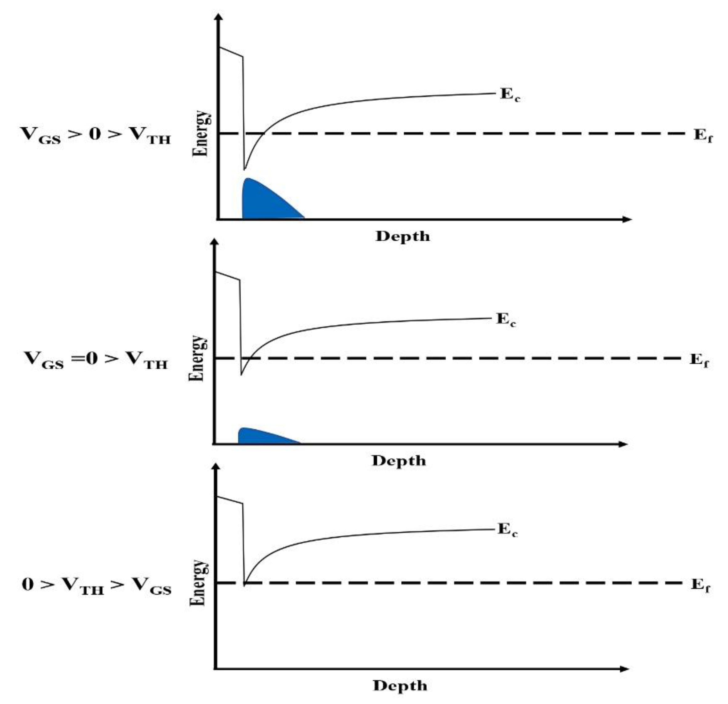
As said previously, when no bias voltage is applied from the gate to the source at the AlGaN/GaN interface, i.e., VGS = 0 V, the 2DEG channel exists. This kind of HEMT is known as a normally-on HEMT or a depletion-mode (D-mode) HEMT. It signifies that a current may freely flow between the source and the drain. It also indicates that the AlGaN/GaN HEMT’s threshold voltage (VTH) is less than 0 V, requiring a VGS to deplete the 2DEG and switch off the HEMT, as shown in Figure 15. Meanwhile, this feature is also one of the primary problems for the state-of-the-art AlGaN/GaN HEMTs utilized in higher current and power applications [36]. It has several practical limitations, including a high consumption, possible electrical safety risk, intrinsic fail-safe functioning, and complex circuit layout [32,36]. As a result, a normally-off operation, or an enhance-mode (E-mode) HEMT, is needed due to a high and positive threshold voltage (VTH).
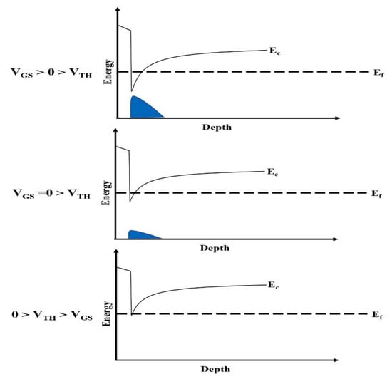
Figure 15.
The band diagrams for the three locations of the 2DEGs VGS > 0 >VTH, VGS = 0 > VTH and 0 > VTH > VGS.
2.2. Lateral and Vertical GaN Power Transistors
Power transistors based on GaN are considered for two types of design: lateral and vertical structures. The lateral structure of the GaN HEMT is illustrated in Figure 16, where 2DEG formed at the AlGaN/GaN heterostructure interface. A high electron mobility (2000 cm2/Vs) and electron velocity (1.3 × 107 cm/s saturation velocity and 2.5 × 107 cm/s peak velocity) characterize the AlGaN/GaN structure. Furthermore, due to a significant spontaneous and piezoelectric polarization, the GaN HEMT structure exhibits a density of sheet carriers over 1 × 1013 cm−2 in III-nitride materials. GaN HEMTs have a low on-resistance because of the device’s carrier density and high electron mobility. This structure is discussed deeply in the normally-off GaN HEMT section.
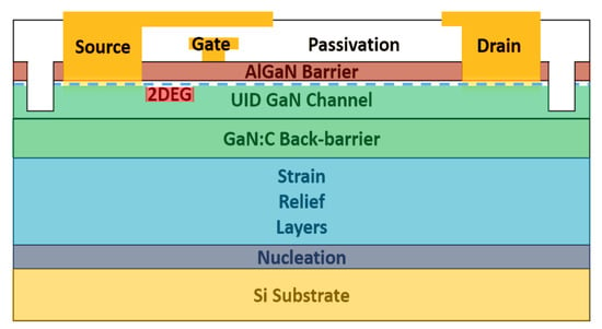
Figure 16.
Typical lateral AlGaN/GaN HEMT structure. Reproduce from IOP science under the terms of the Creative Commons Attribution 3.0 license [36].
Similarly, the vertical layout is beneficial for obtaining a high breakdown voltage and low on-resistance characteristics, as displayed in the current aperture vertical electron transistor (CAVET) in Figure 17 [36]. Here, the drain at the bottom, the gate, and the source are on the top of the structure. The gate controls the current via an aperture among the current blocking layers (CBLs) into the drain, where vast amounts of material flow, which is commonly produced by an isolation implantation or P-type doping of the GaN layer. The AlGaN/GaN layer’s horizontal high mobility electron channel is combined with a thick GaN drift region to obtain a low RON and a high breakdown voltage. Compared to the lateral designs, vertical devices into the bulk material of the device maintain the blocking voltage in the vertical direction, resulting in a lower chip area for a particular operation current.
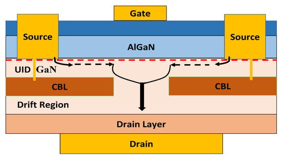
Figure 17.
Vertical CAVET AlGaN/GaN HEMT structure. Reproduce from IOP science under the terms of the Creative Commons Attribution 3.0 license [36].
3. Normally on and off GaN HEMT Power Device Structure
3.1. GaN HEMT Technology (Normally on)
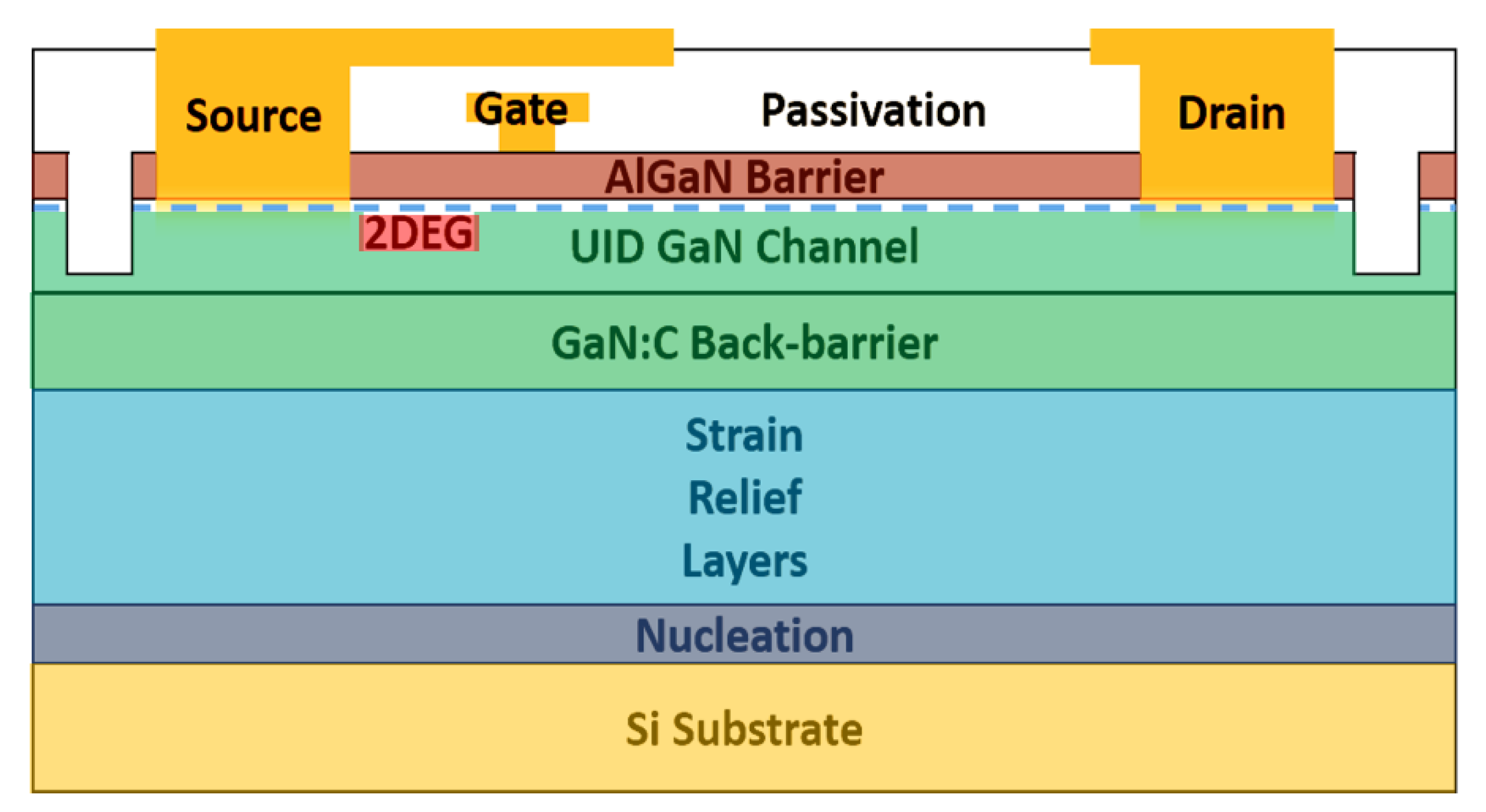
When the AlGaN/GaN HEMT structure is normally on, it is known as the depletion-mode (D-mode) structure. Figure 18 illustrates one of the examples of it. Where the buffer layer (1–5 µm) is deposited on the substrate for compensating the lattice mismatch stress, after that, to form a heterojunction, the GaN (UID) layer, AlN layer (0.7–1.2 nm), and AlxGaN1-xN barrier (15–30 nm) layer is deposited. The thickness and Al molar fraction x of the AlxGaN1-xN (usually 0.15 to 0.4) varies to maintain the number of acceptable electric charges under the relaxation’s critical thickness [37]. The heterojunction’s energy bands are bent downward to produce a quantum well with a sharp, where electrons of a high intensity are confined at the interface of AlGaN/GaN due to a bandgap offset and the polarization impact of AlGaN/GaN [38]. Then, the 2DEG channel generates the high-density current from the Ohmic-contact source to the drain [39]. Consequently, a Schottky gate is needed for the pinching off the 2DEG channel, which is normally on. When sufficient negative voltages are applied to the devise gate, the height of the Schottky barrier increases, allowing for the conduction band to pass through the AlGaN barrier’s gate region; thereby, the HEMT is turned off. Eventually, for the device surface protection, passivating layers (often SiO2 or SiNx) are required [40,41,42].
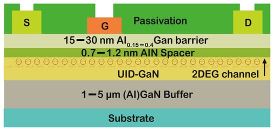
Figure 18.
Device layout for a GaN HEMT structure that is normally on.
3.2. GaN HEMT Technology (Normally off)
In the field of power conversion, a negative bias is required to turn off the devices, which is the major issue for the normally-on devices. On the contrary, a normally off operation is widely wanted for safety reasons. Consequently, academia and industry (e.g., Gan Systems, Infineon, Panasonic, STMicroelectronics, and On Semiconductors) are working to create and market dependable normally-off HEMTs [43]. Thus, the threshold voltage VTH in AlGaN/GaN HEMT is determined by numerous variables relating to the heterojunction and gate metal characteristics, shown in Equation (15) [44]:
where between the gate metal and the AlGaN barrier layer, φB(x) denotes the Schottky barrier height, denotes the polarization charge at the interface of the AlGaN/GaN, ΔEC(x) denotes the conduction band discontinuity at the interface of the AlGaN/GaN, denotes the AlGaN layer permittivity, denotes the permittivity vacuum, denotes the AlGaN thickness, ND denotes the doping, denotes the electric charge, and x denotes the Al content in the barrier layer. As ns increases at a zero bias, more significant polarization discrepancies between the AlGaN and GaN and thicker AlGaN barriers result in a more negative VTH. Hence, it is clear from the equation that the AlGaN barrier layer or modifying Schottky barrier height relies on the thickness and Al content to tune the VTH. Therefore, various approaches have been suggested for obtaining the normally-off GaN HEMTs: the (a) cascode configuration, (b) fluorine implantation and thin/ultrathin-barrier, (c) p-GaN Gate, and (d) recessed gate.
3.2.1. HEMTs with Cascode Configuration (Normally off)
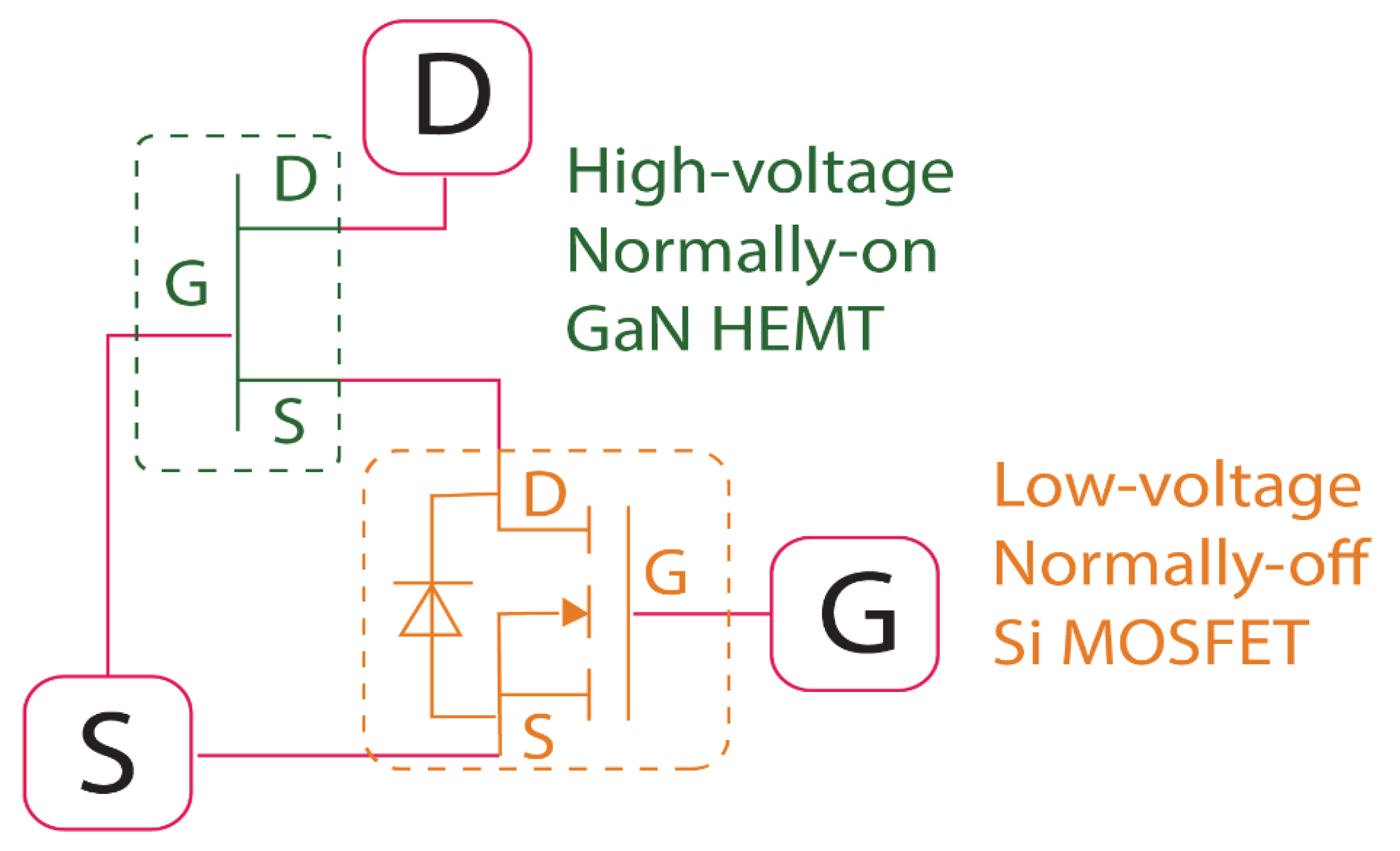
Figure 19 reflects a cascode setup of high-voltage normally-on GaN HEMTs and low-voltage normally-off Si MOSFETs [45,46]. When the VTH of a Si MOSFET less than the positive gate-to-drain voltage is applied to the system, the GaN HEMT’s gate-source voltage is 0 V; as a result, the opening of a GaN HEMT is normally on. By contrast, deactivating the Si MOSFET results in the GaN HEMT having a significant negative gate to source voltage, thus, the 2DEG channel is pinching off. Evidently, the cascode setup generates a positive VTH for regulating the GaN HEMT switch that is normally on. Additionally, normally-off GaN HEMTs with the cascode design are commercially available at 600 V [43,45]. However, the parasitic effects of the packing and the high-temperature stability of the Si MOSFETs remain significant disadvantages [47,48]. If the GaN HEMT has a relatively high on-resistance compared to the Si MOSFET, the “cascode” configuration performs well at that time. In fact, since the on-resistance increases with the rated breakdown voltage, the “cascode” approach is advantageous when the normally on GaN HEMT is one of a high-voltage, and the Si MOSFET is low-voltage [49]. As an illustration, the Si MOSFET will provide just a 3% on-resistance to a 600 V GaN HEMT “cascode”. On the contrary, for a lower targeted breakdown, the on-resistance of the GaN HEMT decreases; thus, the Si MOSFETs contribution becomes significant. Hence, the “cascode” approach is practically advantageous for applications above 200 V [49].
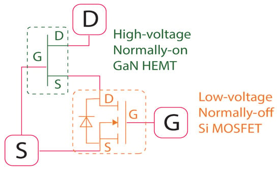
Figure 19.
Normally-off HEMTs with cascode configuration structure.
3.2.2. HEMTs with Fluorine Implantation and Thin/Ultrathin Barrier (Normally off)
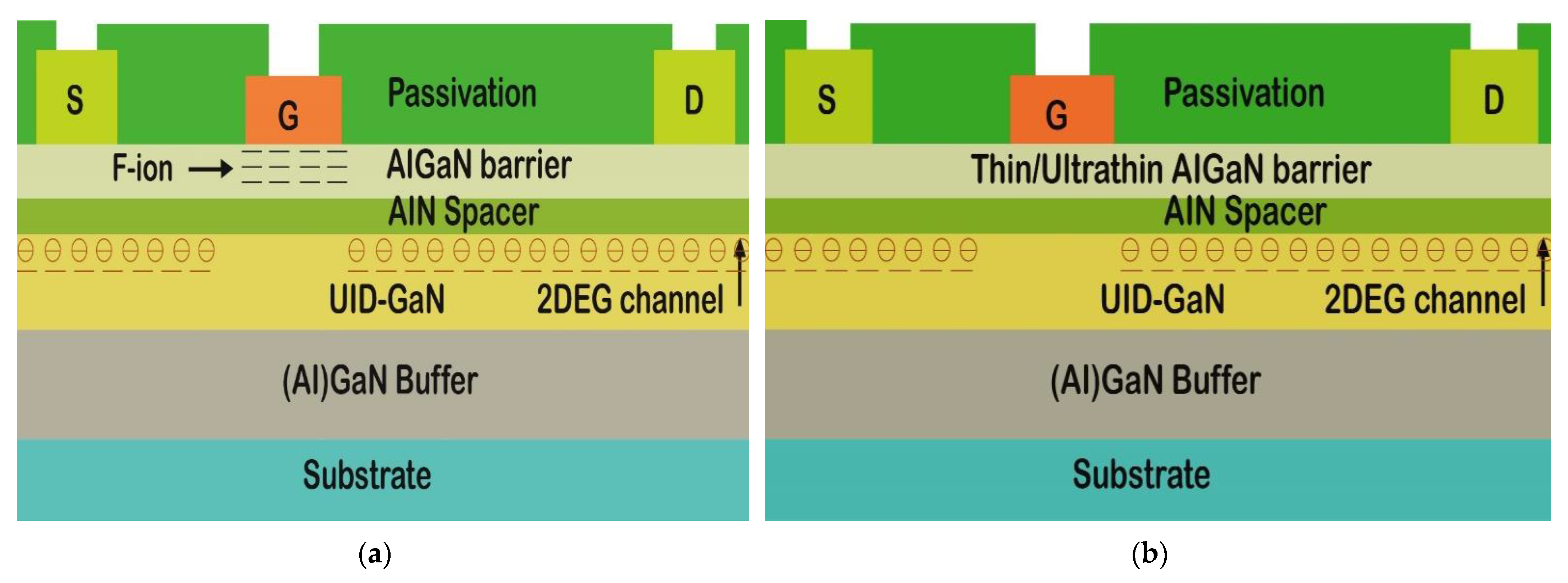
Figure 20a shows an alternative method of performing the normally-off operation to avoid the dry etching, which could cause damage to the device operation. Due to their considerable electron-negativity, fluorine given by the ion implantation and in the AlGaN layers may easily boost the AlGaN barrier electron potential and empty the 2DEG channel [50]. Likewise, by adjusting the height of the AlGaN conduction band, the 2DEG can be depleted by a GaN HEMT design with a thin/ultrathin barrier [51,52], as displayed in Figure 20b. When the AlGaN barrier thickness falls below a critical value, the VTH shifts to a negative bias in the recessed-gate configuration. However, in various application issues, like for fluorine gates, the injection method must be repeatable, and for thin barrier HEMT designs, the output current is low, restricting these two devices [51,53].
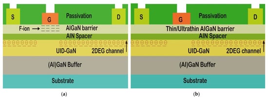
Figure 20.
(a) Normally-off HEMTs with fluorine implantation structure.; (b) normally-off HEMTs with thin/ultrathin-barrier structure.
3.2.3. HEMTs with p-GaN Gate (Normally off)
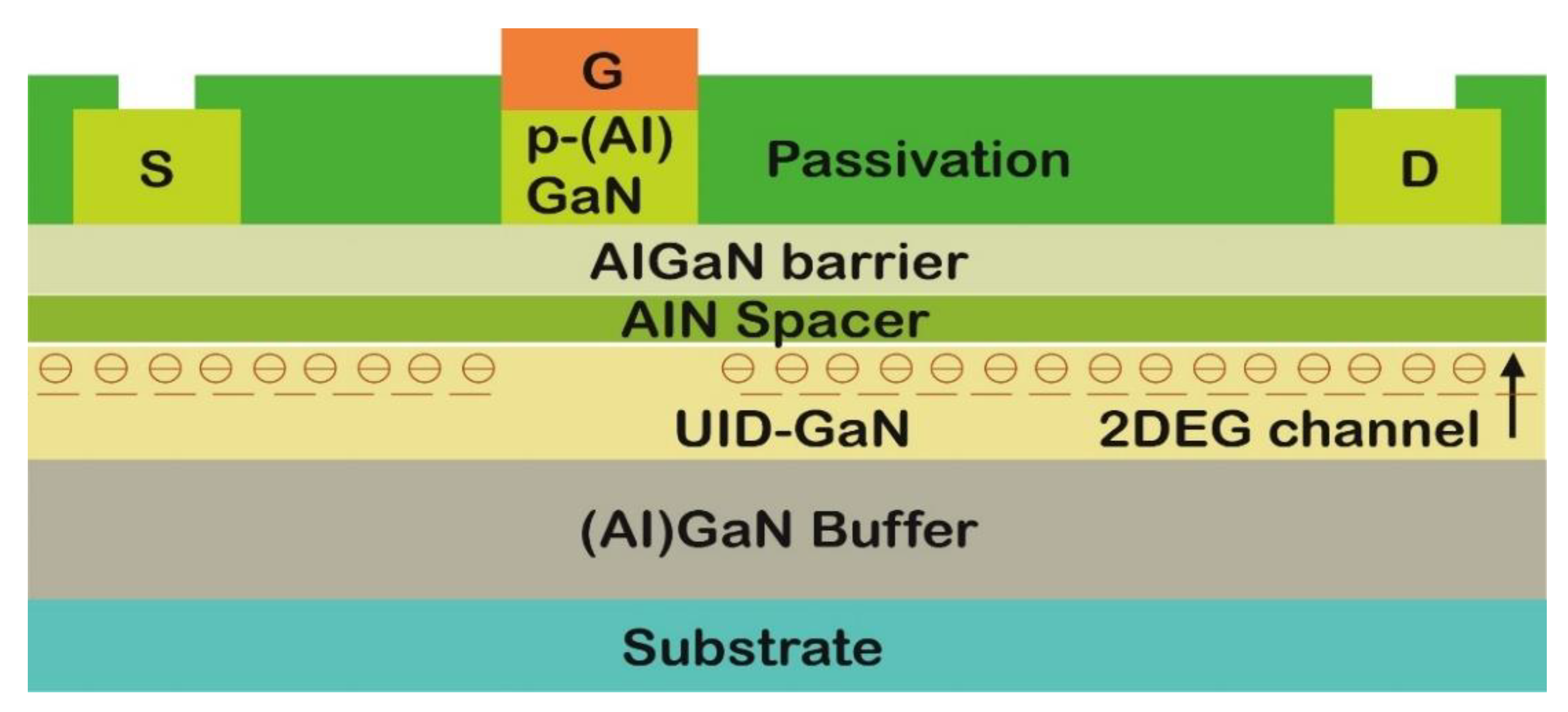
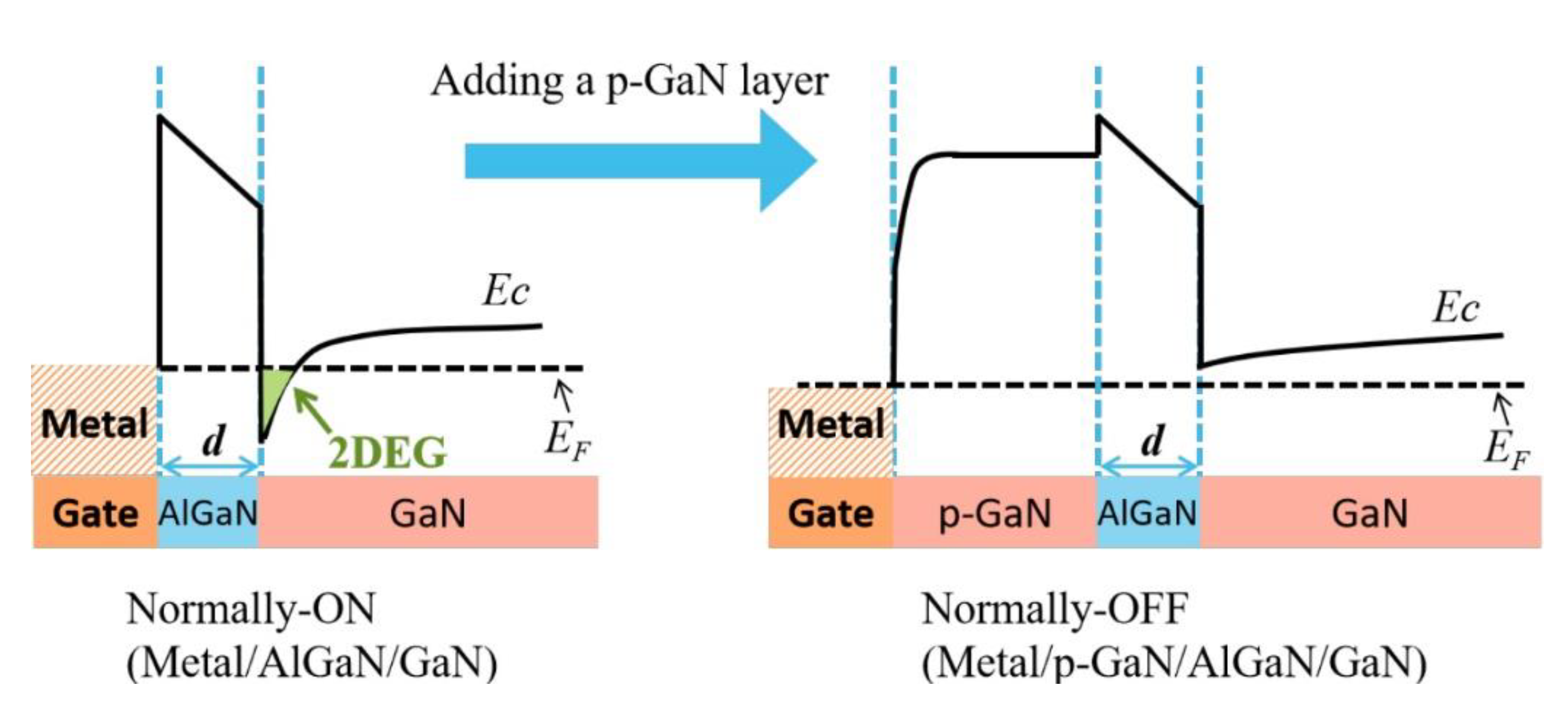
A p-GaN (or p-AlGaN) layer is applied to the AlGaN/GaN heterostructure at the gate region. As illustrated in Figure 21, it is probably the most promising technique to accomplish a normally-off operation [54,55,56]. In fact, it is presently the only commercially available normally-off GaN HEMT technology. GaN HEMTs of this sort have received much attention from the scientific community and the industry. The p-GaN gate HEMTs working principle is generally represented in Figure 22. The AlGaN conduction band is elevated by the p-GaN cap layer on the AlGaN, resulting in 2DEG depletion. Hence, it is possible to obtain the device’s normally-off mode [57]. Earlier, Uemoto et al. [55] proposed a GaN HEMT with a p-AlGaN gate that is normally off, with a VTH of 1.0 V and a BVDSS of 800 V.

Figure 21.
Normally-off HEMTs with p- GaN (or p-AlGaN) layout.
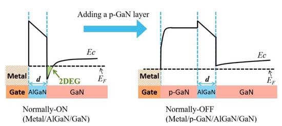
Figure 22.
Metal/AlGaN/GaN energy band diagram with and without a p-GaN gate under equilibrium. Reproduced with permission [57]. Copyright 2017, Elsevier.
The characteristics of the AlGaN/GaN heterostructure should be specified appropriately to enable an effective depletion of the 2DEG and a high VTH (VTH > 0) [48,49,50,51,52,53,54,55,56,57,58,59,60]. The layer thickness of the AlGaN barrier is usually between 10 and 15 nm, whereas the content of Al is between 15 and 25%. For the effective depletion of 2DEG, a high amount of doping in the p-GaN layer (>1018 cm−3) is frequently needed [61]. In this regard, increasing the Mg electrical activation is one of the most critical factors in improving the threshold voltage VTH of the p-GaN layer for a specific Mg concentration. Adequate growth parameters for the p-GaN layer and annealing conditions may achieve the latter goal [62,63]. On the contrary, because of the high energy of ionization (in the range from 150 to 200 m eV) of Mg as a p-type dopant, i.e., an acceptor, obtaining a high activation of Mg in p-GaN is problematic [64,65]. In most cases, an acceptor concentration of 2–−5 × 1019 cm−3 is employed, roughly two orders of magnitude more than the concentration of holes. A greater Mg concentration in p-GaN might cause the layer’s crystalline quality to deteriorate, reducing the electrically active acceptors [66,67]. As a result, in the p-GaN gate HEMTs, getting a high VTH is difficult. Earlier, a Pd-based Ohmic gate was implemented on the cap layer of p-AlGaN, which improved the device’s hole injection and current capabilities. Therefore, the transistor was also known as a “gate injection transistor” (GIT) [55]. The GaN–GIT structure was modified to a hybrid drain-embedded GIT (HD-GIT) by Kaneko et al. [68] The Panasonic group contains a p-doped GaN area adjacent to the ohmic drain. The injected holes discharge the trapped electrons near the drain edge in the off-state from the p-GaN layer, which helps prevent the current collapse. Compared to the standard GIT structure, this new modification boosts the breakdown voltage to 850 V with a slight increase in the device’s leakage current and the on-resistance of 2.6 mΩ·cm2.
In contrast, the metal/p-GaN/AlGaN/GaN system TCAD simulations indicate that on the p-GaN, a Schottky metal gate must have a higher VTH and less leakage than an Ohmic gate [55,63,64]. In the on-state, Meneghini et al. [60] demonstrated that a Schottky gate based on WSiN to the p-GaN rather than a typical Ni/Au Ohmic contact could improve the gate voltage swing of a transistor and lower the gate leakage current by roughly four orders of magnitude. Generally, the continuous power consumption of GaN HEMTs is due to the gate leakage and heat generation in the gate driver. The lack of a considerable gate side current injection due to the significant Schottky barrier is thus essential for HEMTs with a p-GaN gate for a decreased power consumption. Because of this, on the p-GaN, the Schottky gate is preferable over the Ohmic gate solution nowadays. Furthermore, several data from the literature are shown in Table 3, where some metals have been used in the Schottky gate contact to the p-GaN. Subsequently, because of its thermal and chemical durability and processing compatibility, adopting a TiN gate is now a good choice [69]. Eventually, several device and reliability difficulties still need to be investigated further, such as the low VTH, high gate leakage currents, the poor gate BV, and the influence of fabrication techniques on the device’s performance [57,70].

Table 3.
Survey of literature data on different Schottky Contact.
3.2.4. HEMTs with Recessed Gate (Normally off)
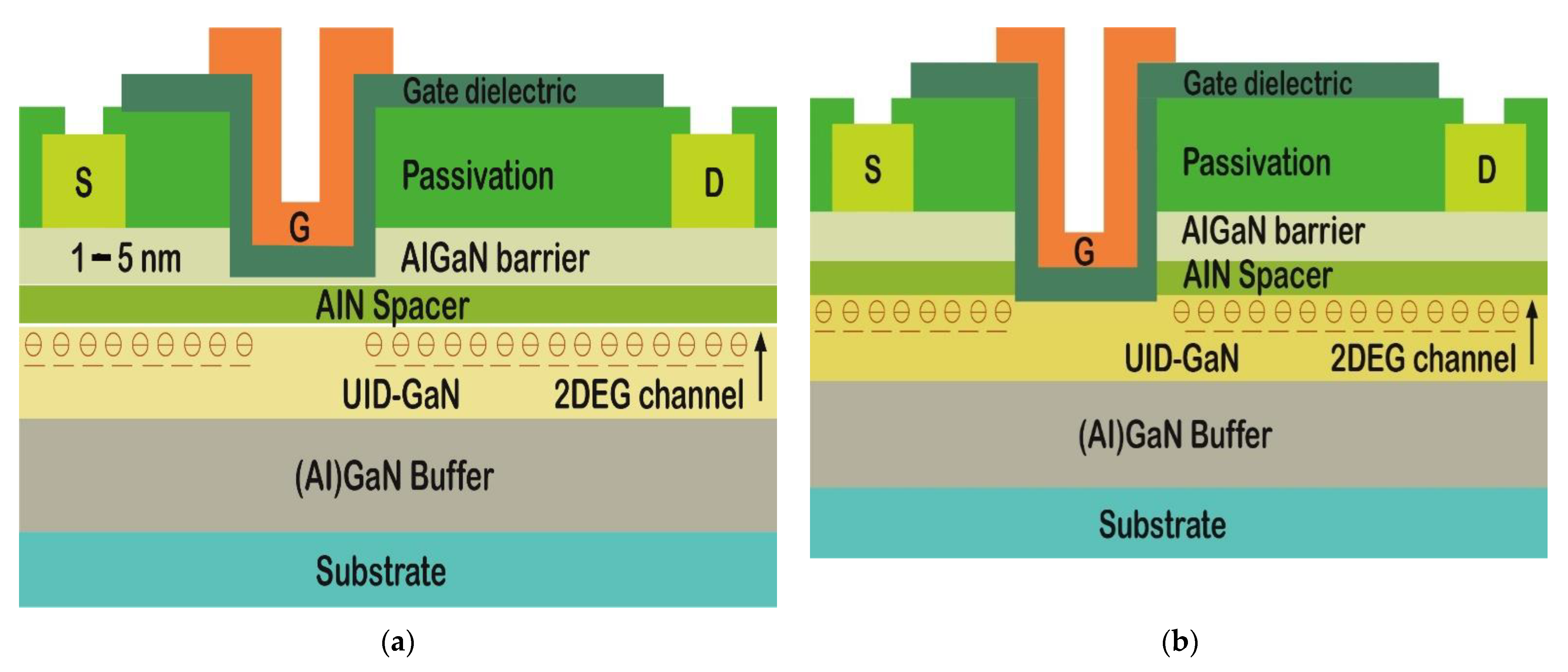
This method reduces the layer thickness of the AlGaN barrier under the gate via a plasma etching, which is the last option offered for achieving an HEMT (normally off) [90]. Because the leakage current of the gate is caused by a tunneling phenomenon that is very sensitive to the barrier layer thickness and uniformity, this approach necessitates a perfect control of the AlGaN etching process. Furthermore, etching-induced damage might increase the leakage current of the gate and non-uniformity effects in VTH [91]. Additionally, there are two types of gates recessed available such as the slight MIS-HEMT of the recessed-gate design underneath the gate dielectric, a thin AlGaN barrier, and the complete MIS-FET of the recessed-gate design, known as a MOS-HFET hybrid, as shown in Figure 23a,b [92,93].
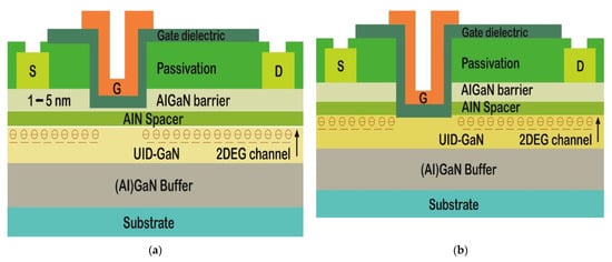
Figure 23.
(a) Normally-off HEMTs with slight MIS-HEMT of recessed-gate design; (b) normally-off HEMTs with complete MIS-FET of recessed-gate design.
Standard MIS-FETs may obtain an E-mode performance by entirely eliminating the AlGaN barrier layer underneath the gate, resulting in the device turning off at a zero gate voltage. Whenever the positive voltage of the gate exceeds VTH, an accumulation layer of an electron forms at the interface of the gates, which operates the devices’ conductive channel and is switched on. It has benefited from a high threshold voltage (VTH) but suffers from a decrease in the channel mobility () due to rough surfaces in the recessed region and electrically active faults in the MIS structure. In addition, a poor channel mobility will raise the device on-resistance (RON) and system power consumption. Therefore, a slight MIS-HEMT of the recessed-gate has been offered to improve the device’s channel mobility () and decline its on-resistance (RON), where the thin layer of the AlGaN barrier will hinder the 2DEG channel from the MIS interface. As a result, the channel mobility () increased and reduced the on-resistance (RON) [94]. Thus, the channel mobility () was defined as Equation (16):
Here, Lg and W donate the channel length and width, while Cox donates the gate insulator capacitance per unit area. Moreover, Fiorenza et al. [95] have evaluated in MISHEMTs of the recessed gate the field-effect mobility by using gate insulator SiO2 with several variables (the roughness of the surface, the temperature, the field of electric, the quality of the dielectric, and so on). This study demonstrated in the insulator/GaN system the necessity of reducing the interface state density to enhance the field effect’s mobility and decrease the precise on-resistance. Eventually, these two recessed gates improved the threshold voltage, device performance, channel mobility, the reliability of the device, and overcame the gate leakage issue [96,97,98]. Additionally, the gate dielectric for the gate recessed depends on several characteristics, such as the permittivity, the (Al) GaN band offset, the bandgap, and the insulator chemical stability [38,94,95]. Especially for power-switching devices, a wide bandgap material is also significant. The (Al) GaN band offsets are required to reduce the gate leakage currents appropriately, even while operating the forward gate bias. On the contrary, a high permittivity value is advantageous for obtaining high transconductances [43]. In the case of MIS-HEMTs, the capacitive contribution of the gate dielectric is minimized by a high permittivity dielectric, facilitating a stronger connection between the 2DEG channel and the gate and therefore maintaining high transconductances, which is especially important for RF devices. In addition, compared to Schottky gate HEMTs, the high permittivity materials may limit the changing of the values of the threshold voltage from positive to negative of normally-on MIS-HEMTs, which helps lower the static power usage and improve the performance and the energy efficiency of the device [99].
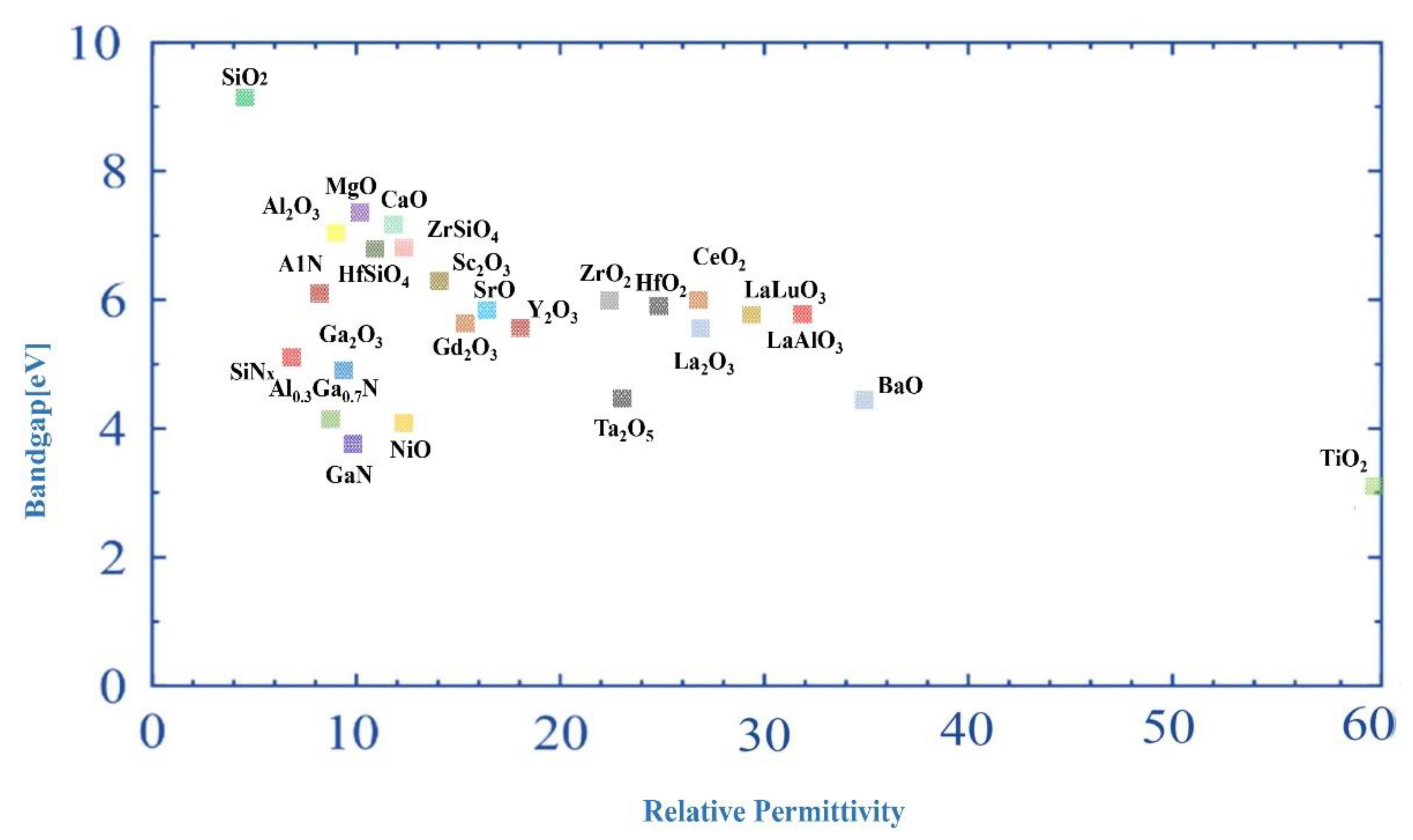
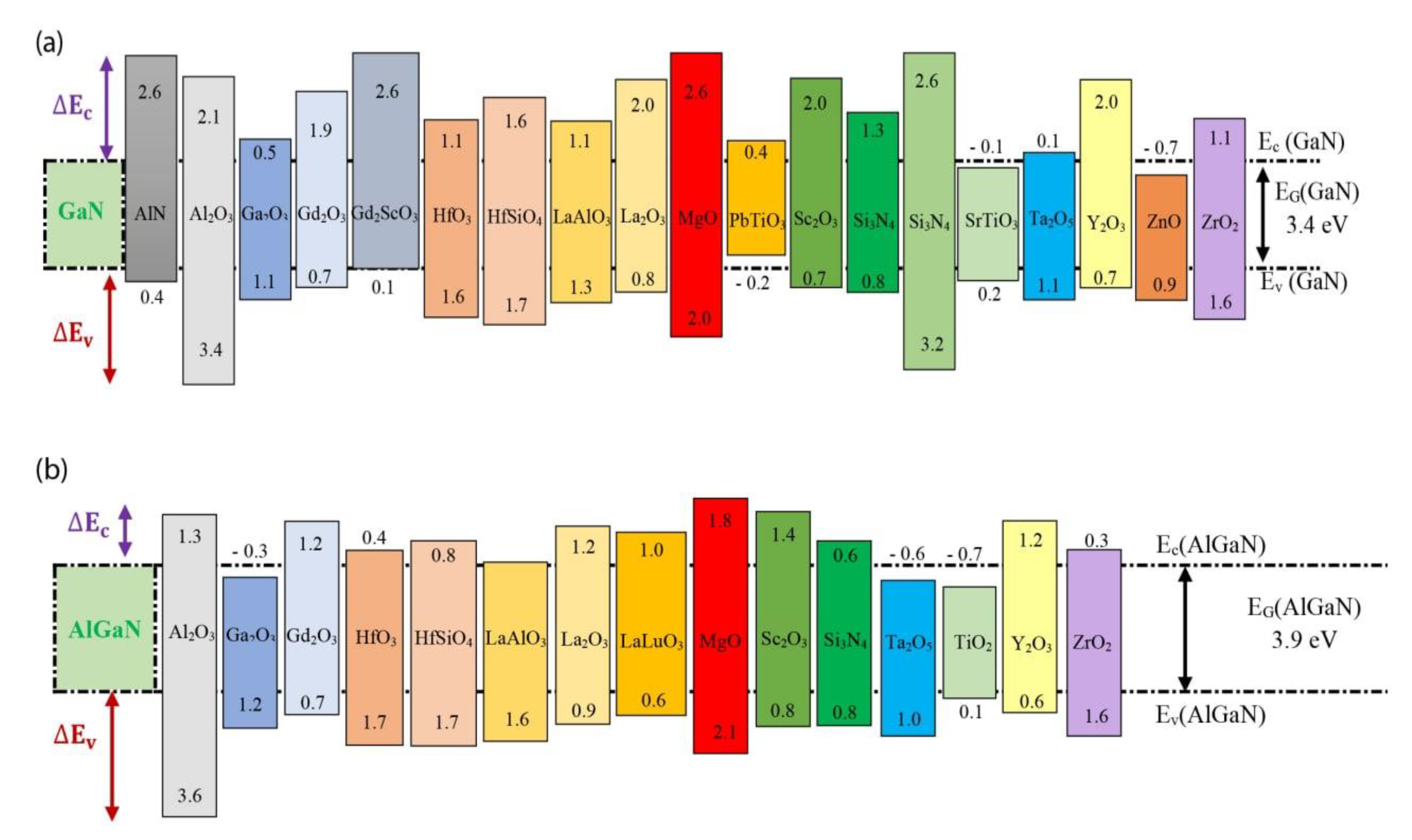
In GaN-based insulated-gate transistors, Figure 24 demonstrates the bandgap-permittivity connection for nitride compounds and the insulators for different gate dielectrics [38,95,96]. Figure 25a illustrates that Robertson et al. [100] calculated the insulators on the GaN band offsets; they were the first to forecast the band alignment of the GaN and the insulators using charge neutrality levels (ECNL) calculations. Figure 25b shows the dielectrics on the Al0.3Ga0.7N band offsets recently obtained by Reddy et al. [101] using the same approach. As a gate dielectric, SiO2 on AlGaN/GaN MIS-HEMTs was first implemented by Khan et al. [102] and they noticed that it enhances the gate voltage swing capabilities and controls the leakage currents in the gates for its attractive characteristic-like large band offset to (Al)GaN, the chemical stability, and the large bandgap.
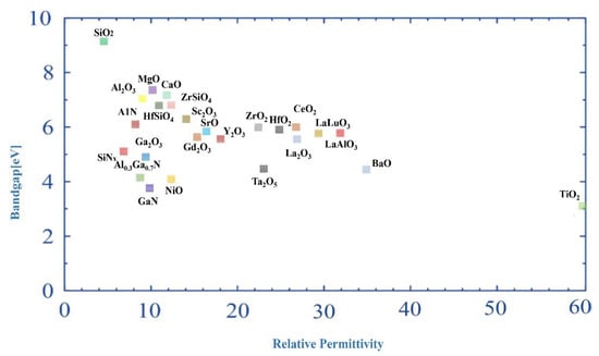
Figure 24.
For primary insulators and GaN compounds, the energy bandgap (eV) vs. permittivity is shown. Reprinted with permission [42]. Copyright 2017, the author(s). Published by Elsevier.

Figure 25.
Various dielectric materials regarding (a) GaN [100] and (b) Al0.3Ga0.7N [101] have different valence and conduction band offsets (EV and EC).
In contrast, for MIS gate designs utilizing dielectrics such as Ga2O3, SiNx, because of its small conduction band offsets, resulted in large gate leakage currents [103,104,105]. Likewise, the minor AlN and (Al)GaN lattice mismatch has been shown in a few investigations, whereby it is appropriate for the gate insulator and passivation layer [106,107]. Moreover, numerous high-permittivity dielectrics have been used in the MIS gate architectures of GaN HEMTs [108], including HfO2, ZrO2, Ta2O5, La2O3, CeO2, and TiO2 [109,110,111]. Thus, Table 4 represents the data gathered from the literature study of normally-off HEMTs with a recessed gate where several types of gate insulators (SiN, SiO2, Al2O3, and processing (PECVD, LPCVD)) are shown.

Table 4.
Survey literature data on difference types of gate insulators and processes.
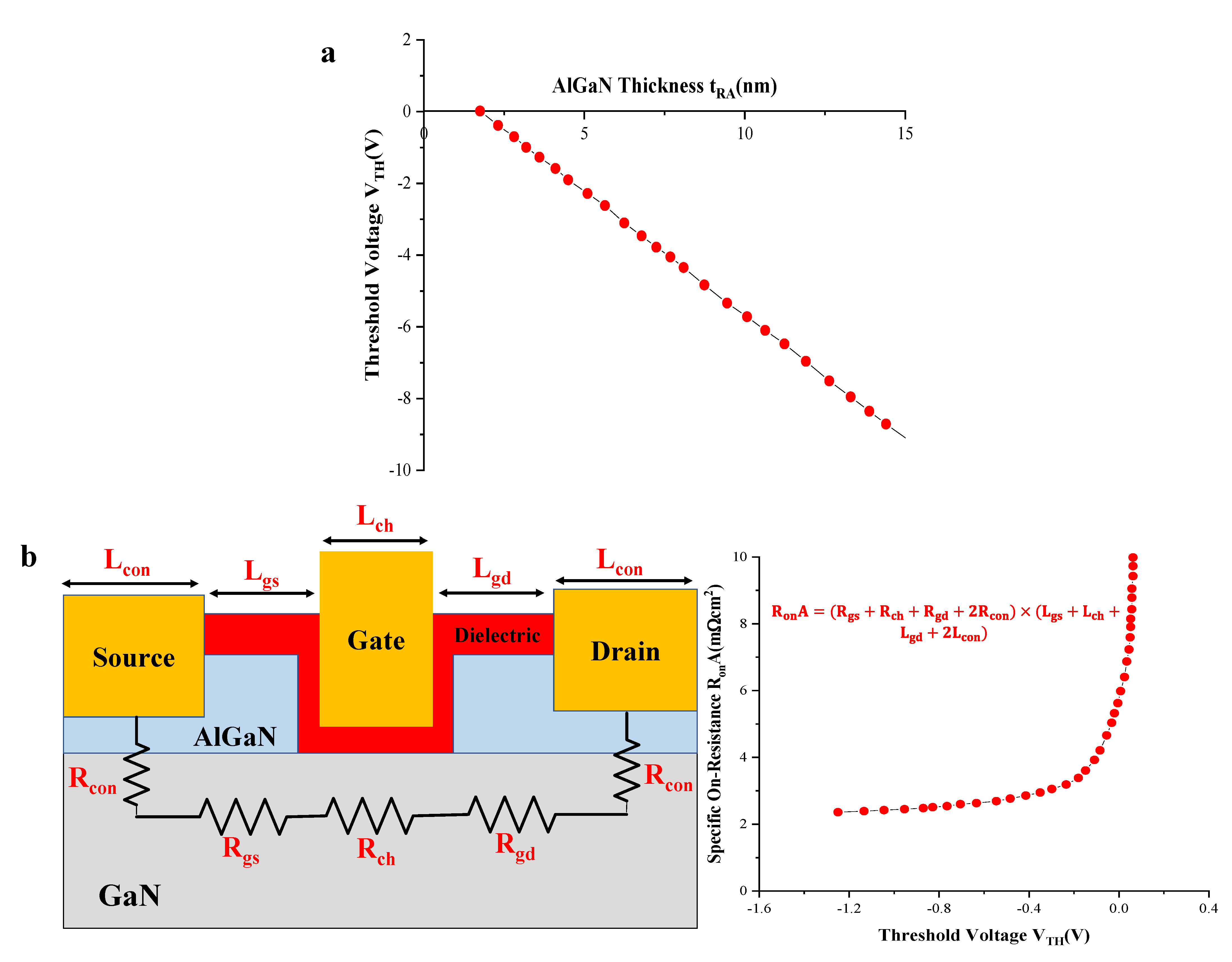
Subsequently, the AlGaN thickness is another important factor for the threshold voltage (VTH). Medjdoub et al. [132] had shown the relation between the AlGaN thickness with a threshold voltage. From Figure 26a, notice that if the AlGaN thickness (tRA) reduces, the VTH increases. Similarly, other authors, Saito et al. [133], presented the relationship between the VTH and the specific on-resistance (RonA) by calculating the equation, as displayed in Figure 26b. On the contrary, the on-resistance (RONA) will be increased if the 2DEG mobility is decreased. Thus, from Figure 26b, the equation for calculating the specific on-resistance (RonA) is denoted by Equation (17),
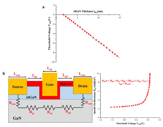
Figure 26.
(a) The AlGaN layer thickness and gate threshold voltage relation. (b) In the recessed-gate GaN HEMT, the calculation of specific on-resistance and the relation between the threshold voltage and the specific on-resistance. Reprinted under the open access policy from Bentham Open [132].
Additionally, the field plate has used a device structure to reduce the current collapse. For GaN-based devices, current collapse is a well-known phenomenon that results in a trade-off between the breakdown voltage and the on-resistance by inserting the source-gate field plate; the electric field at the gate-drain edge is redistributed [134,135,136], as shown in Figure 16. The current collapse is discussed in the below segment.
4. Reliability of GaN HEMTs
4.1. Degradation Creation
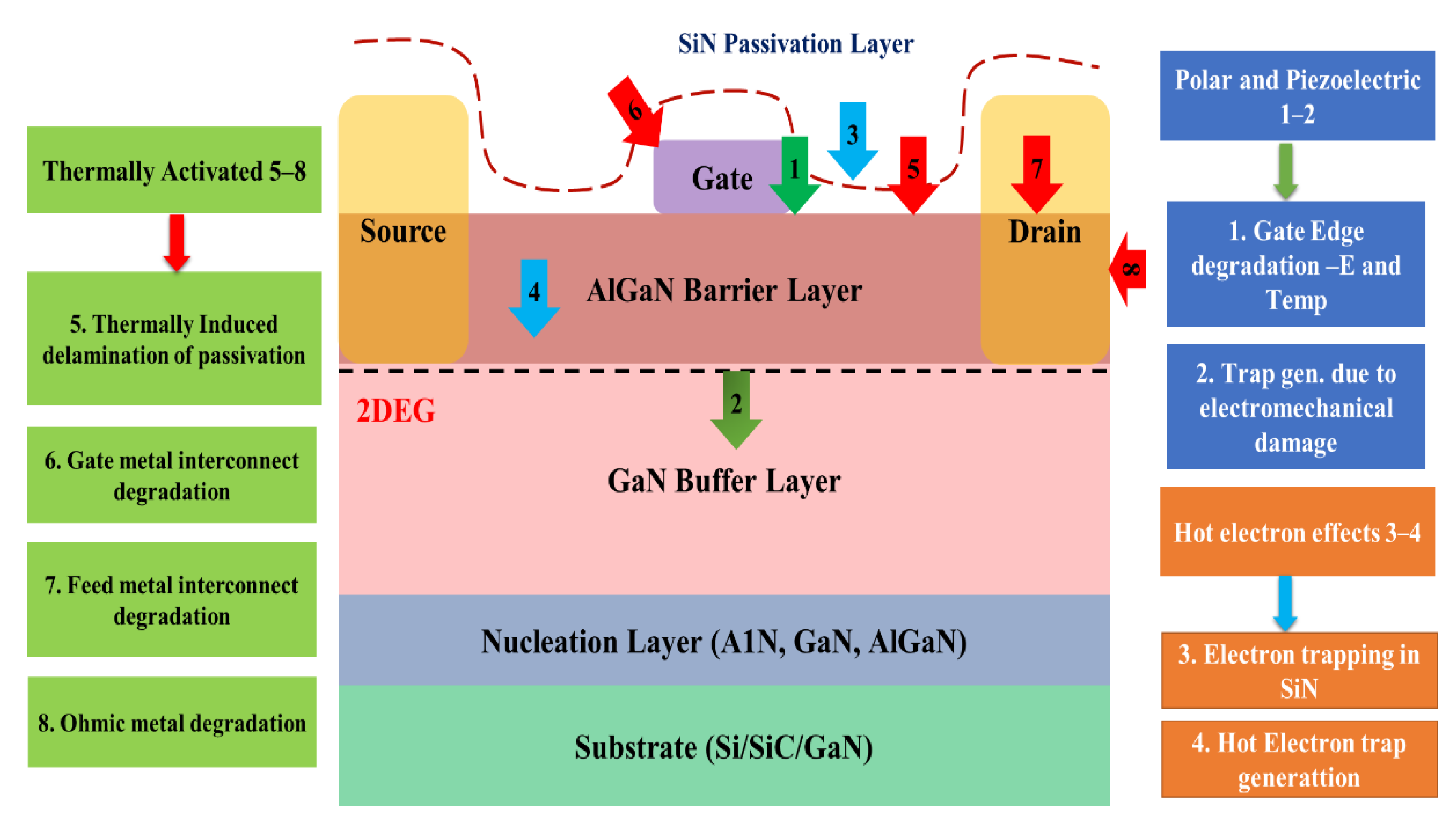
While GaN HEMTs have improved remarkably, several material-related challenges must be resolved before they are revealed as a reliable and sustainable technology. AlGaN/GaN HEMTs’ actual device performance has not yet reached the theoretically predicted levels. Even on unaged GaN HEMTs, parasitic effects could be noticed that degrade the performance metrics but do not significantly impact the reliability. Nevertheless, over time or under aging stresses, the degradation processes that accelerate with time impair not only the electrical response but also the device’s resilience and dependability, resulting in shorter lifetimes and failure. The GaN industry’s principal aim is to improve the dependability of its products while also reducing the parasitic effects. Further degradation difficulties with GaN devices include thermal mismatches, heteroepitaxy, and polarization effects with the substrate, all of which are inherent to the material. Compared to other conventional technologies, AlGaN/GaN HEMTs can work at an extremely high bias, electric fields, and temperatures. Figure 27 demonstrates the various types of degradation affecting AlGaN/GaN HEMTs [137,138].
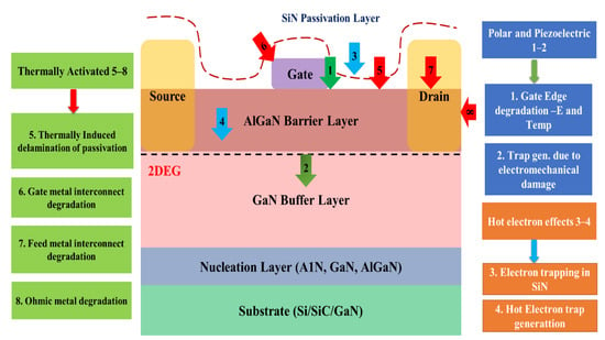
Figure 27.
Several degrading problems affect AlGaN/GAN HEMTs with their origin. Reprinted with permission [138]. Copyright 2010, Cambridge University Press, and the European Microwave Association.
It is important to note that five to eight issues are associated with thermally induced degradation processes that have already been reported in other semiconductor systems (SiC, GaAs, Si, etc.). As a result, these failure mechanisms are simpler to explain and exclusive to the metallization scheme which has been adopted. Both three and four mechanisms are connected to the introduction of the hot electrons; it is a usual problem that field-effect transistors of a high voltage face. Other semiconductor devices have been proven to suffer from a deterioration, caused by hot electrons (Si, GaAs, InP, etc.). On the other hand, because of this semiconductor material’s piezoelectric and polar properties, one to two issues are specific for GaN devices; consequently, those processes have not been fully defined or investigated. As a result, the GaN HEMT reliability analysis is a unique issue that needs to be devoted, as well as an in-depth physics-based study. Furthermore, high Schottky-gate leakage currents are also one of the main issues for degrading the device performance and reliability. Thus, the reduction in BVGD raises the noise figure (NF) and decreases the power-added efficiency (PAE) due to the high gate leakage current [139]. In addition, there are numerous mechanisms of gate leakages, including the emission of a thermionic field [140], the emission of thermionic [141], the dislocation-assisted tunnelling [142], the trap assisted tunnelling [143], the Fowler–Nordheim tunnelling [144], the defect hoping [145], the space charged limited current [146], and the Frenkel–Poole emission [147].
4.2. Reliability Issues
These days, researchers focus on enhancing the AlGaN/GaN HEMTs reliability device because of the trapping effect during the AlGaN/GaN HEMT operation. One of the major obstacles causing performance degradation is the trapping effects in AlGaN/GaN HEMTs during operation, causing current dispersion between DC to RF or otherwise, DC to pulsed ID−VD characteristics. Trapping effects like the frequency dispersion of transconductance, the sensitivity of the light, the drain lag and gate lag transients, and the limited microwave power output have all been detected [148].
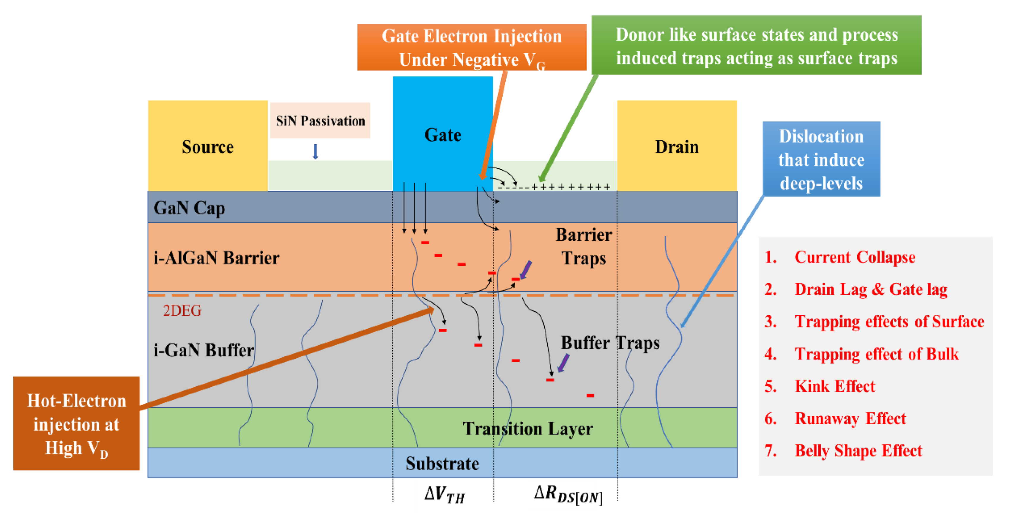
As shown in Figure 28, there are various trapping mechanisms usually seen in AlGaN/GaN HEMTs, such as:
- Under a high negative VGS, barrier traps and a gate electron are injected onto the surface;
- Under a high on-state VDS, the barrier/buffer traps are injected using hot electrons;
- During material growth, the electrons captured by the deep layers are induced.
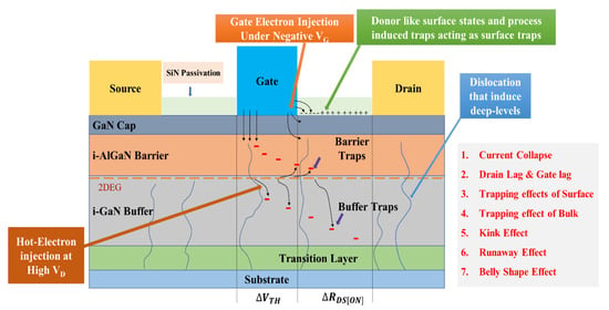
Figure 28.
The AlGaN/GaN heterostructure is shown schematically, with several trapping methods and their effects on device performance. Reprinted with permission [149]. Under the terms of the Creative Commons Attribution 4.0 license.
Figure 28.
The AlGaN/GaN heterostructure is shown schematically, with several trapping methods and their effects on device performance. Reprinted with permission [149]. Under the terms of the Creative Commons Attribution 4.0 license.
4.2.1. Current Collapse
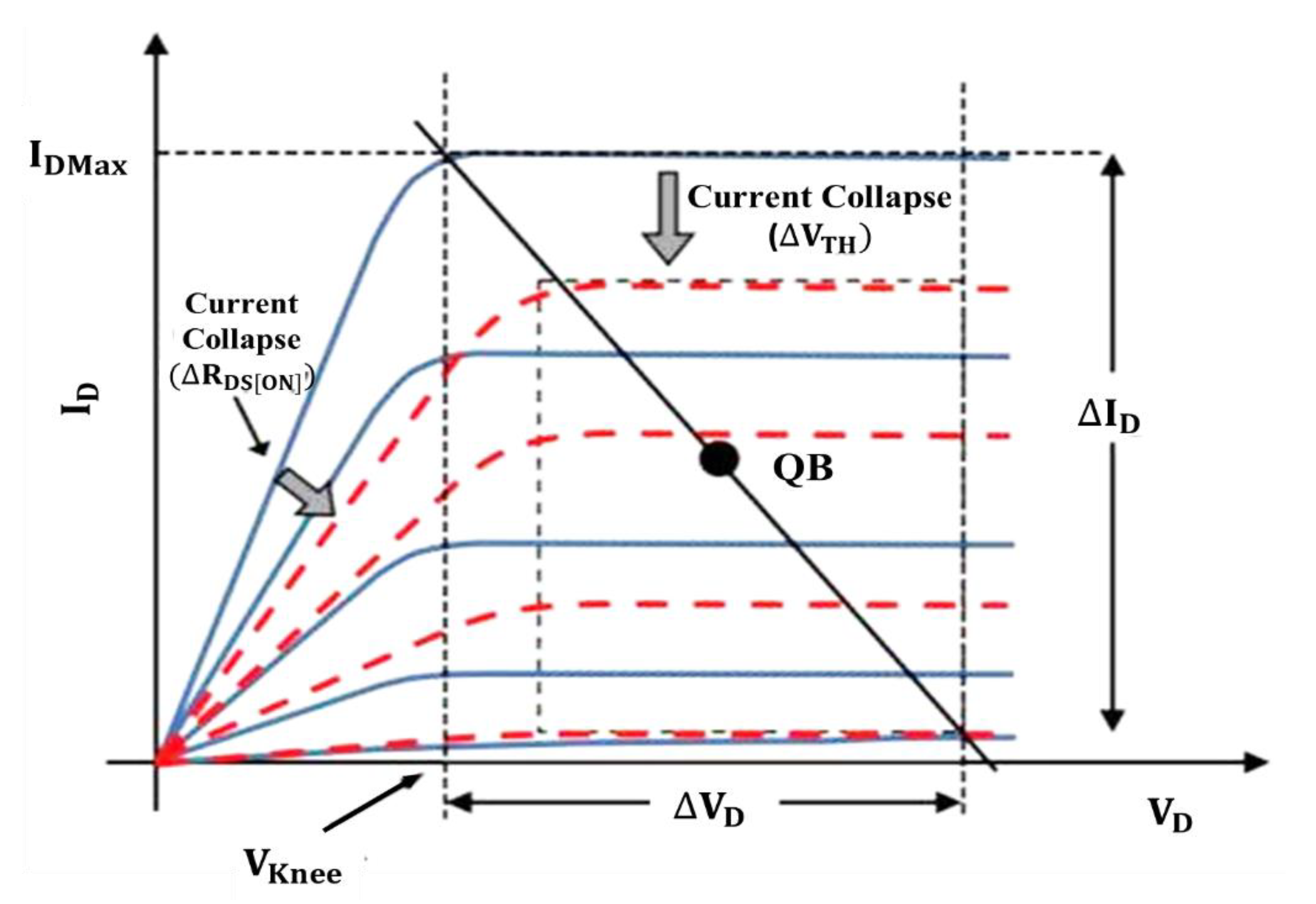
In order to maintain the charge neutrality, trapping electrons reduces in the 2DEG channel the density of the sheet carriers, resulting in a decreased current density in the drain. This decrease in the drain current is referred to as the “current collapse”. M. A. Khan et al. [150] released the first article on AlGaN/GaN HFETs current collapse in 1994. The “drain-lag” and “gate-lag” conditions of the quiescent bias (Q-bias) are the main parameters used to characterize the current collapse phenomena [148]. In Figure 29, the characteristics curve of ID–VD demonstrates the current collapse’s effect on the output power of HEMT. The solid and dotted lines indicate the device’s ID–VD characteristics curve before and after the current collapse phenomena. The current collapse causes the knee voltage (Vknee) to grow as the maximum current decreases (IDmax). It reduces the maximum output power (Pmax) that may be achieved, which is provided by the given equation:
The dissimilarity between the Vknee and the breakdown voltage (BVGD) equals the highest possible voltage swing (). IDmax specifies the maximum current swing. Pmax is depicted in Figure 29 by the shaded region, and the current collapse phenomena have narrowed this operating window. Thus, the main reason for the current collapse is caused by the reduction in positive charges of polarization induced from the heterojunction transistor surface, followed by the loss of an equivalent number of electrons in the 2DEG [151]. RDS[ON] characterizes the current collapse, as illustrated in Figure 29, because the electrons are trapped in the gate-drain access area by the surface, buffer, or barrier traps. Similarly, under the gate are the areas of electron trapping (see Figure 28), resulting in a threshold voltage shift (), which characterizes a current collapse; therefore, the pulsing ID–VD characteristics are caused by a drop in the drain current in the device’s saturation zone, as seen in Figure 29.
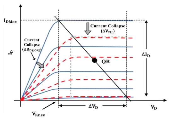
Figure 29.
The ID–VD characteristics curve of HEMT before (solid lines) and after (graded lines) current collapse is shown in this diagram. Reprinted with permission [152]. Copyright 2003, the American Vacuum Society.
Figure 29.
The ID–VD characteristics curve of HEMT before (solid lines) and after (graded lines) current collapse is shown in this diagram. Reprinted with permission [152]. Copyright 2003, the American Vacuum Society.
4.2.2. Drain and Gate Lag
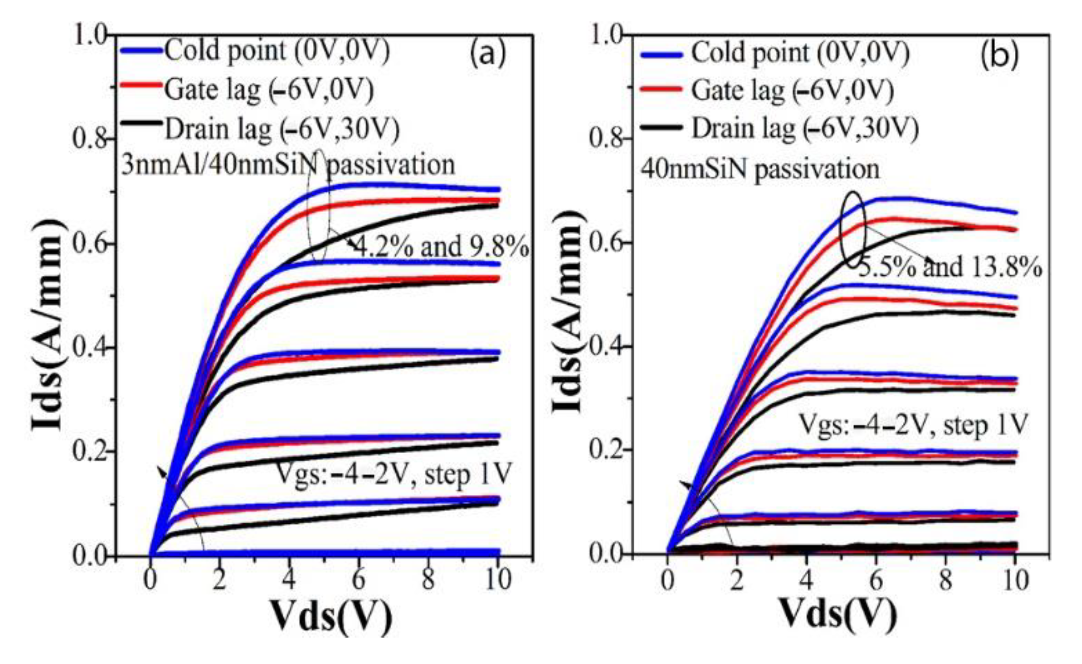
The gate lag refers to the drain current’s transient response to the gate voltage, and a drain lag is the transient response of the drain current to the drain voltage, which remains constant when the drain or gate voltage matches. According to Figure 30, Zhang et al. [153] investigated the magnitudes of collapse between the saturation and the knee voltages for the various quiescent biases. Hence, the collapse considerably reduces the performance near the knee voltage. From curve (a), when VDS = 4.5 V, the collapse percentage was 4.2 and 9.8, respectively, with the Al/SiN passivation layer. On the contrary, the collapse rate increased by a 5.5 and 13.8 percentage, with the SiN passivation layer at the VDS = 5 V, approximately, on the curve (b).

Figure 30.
The gate lag and drain lag of (a) Al/SiN passivated and (b) SiN passivated AlGaN/GaN HEMT devices were measured at different passivation layers. Reproduced with permission [153]. Copyright 2019, the author (s), published by AIP Publishing.
However, the effects of acceptor- and donor-like traps on the HEMT device were analyzed by Tirado et al. [154] The accumulating hole near the surface counteracts the acceptor-like traps, and the device is insensitive to the acceptor-like traps. Therefore, the surface donor-like traps are the primary cause of the gate lag [155]. Figure 31a presents that in addition to the dipole charge owing to polarization-induced charges, the charge due to 2DEG, the charge due to the donor-like trap ionization, and the charge due to the holes accumulating close to the AlGaN surface, the filling and emptying of the donor-like traps in the surface can impact the density of the 2DEG. When a new device is strained, the electrons that directly tunnel through the Schottky gate contact can occupy the donor-like traps and turn them neutral [156]. The 2DEG density is dropped with the reducing donor-like traps due to the charge neutrality criteria, which causes an initial fall in the current in Figure 31b [154], where the drain current instantly rises as the on-state remains stable for a while. After that, until saturation, its soars again. At the final stage, the drain current change is referred to as the delay of the current, known as a gate lag.
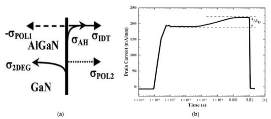
Figure 31.
(a) Diagram of an HEMT device’s space charge element. The two-dimensional electron gas is referred to as σ2DEG, the dipole charge induced by polarization is denoted by ± σ POL1,2, Ionized donor-like traps are referred to as σIDT, and σAH symbolizes the accumulation of holes near the AlGaN surface. (b) AlGaN/GaN HEMT gate lag phenomenon’s transient waveform of the drain current. Reproduced with permission from IOP Publishing [154].
When measured at the turn-on pulsing mode, the observed drain current tends to reduce with time, as shown in Figure 32a. When evaluated at the turn-off pulsing mode, Figure 32b indicates a decline in the drain current when the voltage at the drain returns to 0 V. These two varieties of the drain current curves are frequently referred to as the drain lag [157]. Due to the trapping of the electron in the channel, this current reduction occurred. Some electrons might tunnel through the AlGaN barrier while the device is in the on-state and trapped by deep-level traps. Eventually, to overcome these issues, the passivation layer and field plate had to be used on the device, as presented in Figure 16.
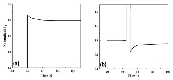
Figure 32.
For AlGaN/GaN HEMTs, the transient waveform of the drain current from the drain lag phenomena. (a) turn-on pulsing mode (b) turn-off pulsing mode. Reproduced with permission [157]. Copyright 2009, the author (s), published by AIP Publishing.
The gate lag measurements compare the prompt and steady-state ID at a constant low field drain voltage (avoid self-heating contributions) while the gate bias is modulated from a quiescent point, usually below the pinch-off voltage ~VG = −6 V, to an open channel condition such as VG = 0 V. At the pinch-off, a high amount of channel electrons are trapped in bulk or surface states, which do not immediately feed back into the channel instantaneously when the gate turns on. With the large-signal recovery time of constants up to the order of seconds, the responsible traps must have a significantly large activation energy and/or be fed by a “slow” conducting mechanism (like hopping) to explain the long time constants. The surface states are believed to dominate in the gate lag since the passivation significantly improves the current response.
For the drain lag measurements, the gate voltage is kept constant at around 0 V, while the drain voltage is shifted from a low equilibrium value of ~10–100 mV to a higher value of 15–30 V. The buffer traps are reported to be dominant here since the devices with higher buffer layer conductivities display lower drain lag ratios. High-drain biases inject electrons into the buffer, where they stay trapped. The passivation has a minimal effect, and the hot electrons can contribute significantly. The recovery time is often in minutes, and the reduction in the knee voltages and ID,max is amplified. The threshold shifts associated with the current collapse are also accounted for with the drain lag effect.
4.2.3. Trapping Effects of Surface
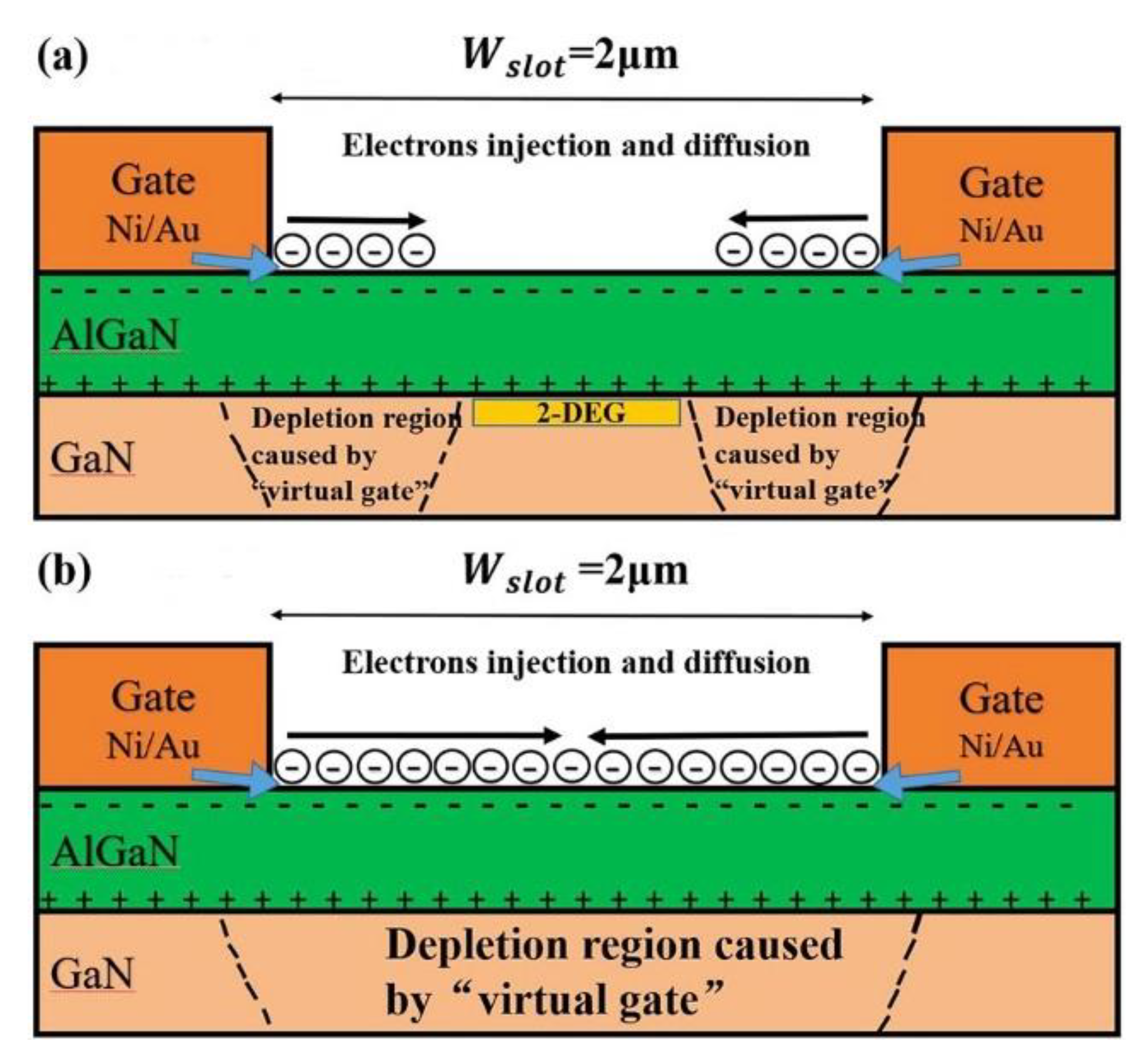
In GaN HEMTs, the effects of surface trapping are commonly used to describe electron trapping on the AlGaN barrier surface. R. Vetury et al. [158] utilized the “virtual gate” idea to describe the current dispersion because of surface trapping on the ungated surface between the drain and gate contacts under negative VGS and a positive drain bias. Thus, Figure 33a illustrates that, at first, due to the presence of a momentous initial drain current, the 2DEG channel must remain in the slot region; from the bilateral metal gates to the AlGaN surface in the slot area, the electrons are injected and captured by the surface states when the off-state gate voltage is applied. Afterwards, from both the bilateral gate edges to the middle of the slot region, the negative trapped surface charges steadily deplete the 2DEG conduction channel, which, acting as a “virtual gate” on both sides, converges at the middle of the slot region, and the entire 2DEG channel in the slot region becomes wholly depleted. Eventually, it has gradually become a complete “virtual gate”, as presented in Figure 33b [159].

Figure 33.
The device layout illustrates (a) electron injection in the slot region and the virtual gate in both areas. (b) the devices become fully virtual gates. Reproduced with permission [159]. Copyright 2019, the author (s), Published by AIP Publishing.
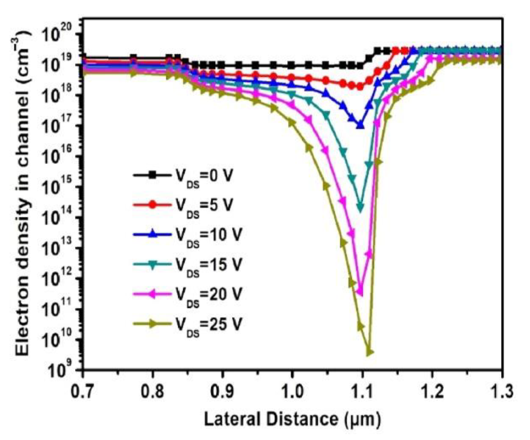
The impact of the virtual gate on the sheet carrier density is observed in Figure 34 [160], where the increased drain voltage at the gate edge of the drain side causes a linear reduction in the sheet carrier density. For this reason, electrons accumulate at the drain side’s gate edge. Consequently, this accumulation of electrons not only influences the channel but also extends towards the lateral axis of the device, for instance, extending the depletion from 1.1 μm to 1.2 μm for the drain voltage from 0 V to 25 V.
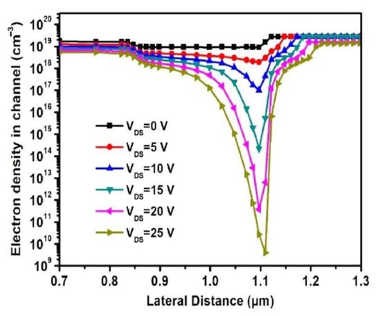
Figure 34.
AlGaN/GaN HEMT sheet carrier density along the channel for different drain voltage. Reproduced with permission [160]. Copyright 2021, Elsevier.
4.2.4. Trapping Effect of Bulk
Bulk traps are traps of electrons which are found in the GaN buffer, AlGaN barrier, or other parts of the device heterostructure, as shown in Figure 27. J. Joh et al. [161] also reported that the injection of an electron into the bulk traps from the gate induced the bulk trapping effect to occur. Thus, X. Zheng et al. [162] illustrated that varying the VGS has bulk trapping effects on the AlGaN barrier traps (TP2) and the GaN channel layer traps (TP1), presented in Figure 35. However, from the gate current (IG), TP2 can capture more electrons if the VGS increases the negative bias voltage. TP2s electron trapping reduces the channel carrier concentration, which lowers the drain current. Additionally, the trapping process of TP2 is speeded up by a higher negative bias voltage of VGS, which decreases the action time of TP2. Meanwhile, TP1 is insensitive to the change in VGS, causing little effect on TP1. Eventually, it is observed that the VGS effect on TP1 is less than on TP2.
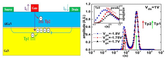
Figure 35.
Trapping process of TP1 and TP2 with various values of VGS. Reproduced with permission [162]. Copyright 2016, Elsevier.
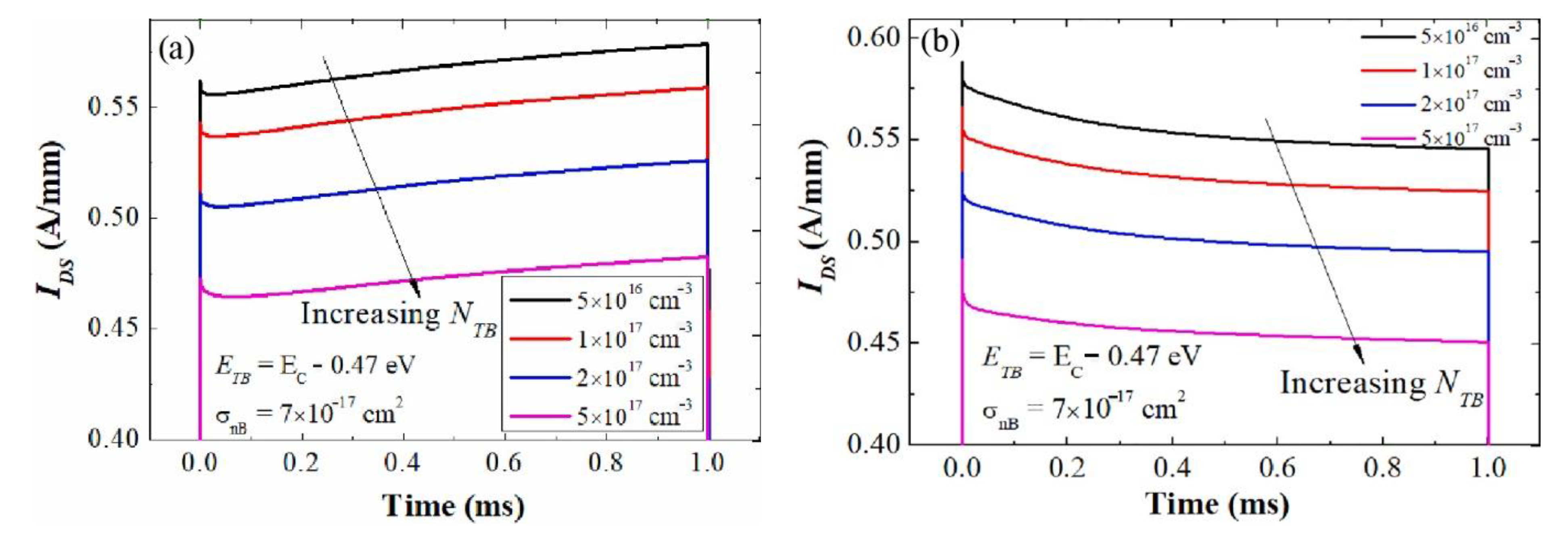
P.V. Raja et al. [163] analyzed the buffer trapping effects on the AlGaN/GaN HEMT device. For the gate lag transient, the VGS pulsed from −3 V to 0 V (from the off- to on-state) with a fixed VDS = 10 V. The gate lag transient is simulated by changing the density of the buffer trap, NTB (from 5 × 10¹⁶ to 5 × 1017 cm−3), with a fixed electron trap at ETB = EC− 0.47 eV and an electron capture cross-section σnB = 7 × 10⁻¹⁷ cm2. As a result, by increasing the NTB, the signal magnitude of the gate transient is reduced, but variations of the transient are unchanged, as presented in Figure 36a. On the contrary, the VGS remains at 0 V, and the VDS is switched from 2 V to 10 V in the drain lag transient. The parameters of NTB and σnB remain the same on the buffer trapping. Consequently, reducing the magnsitude of IDS does not affect the current dispersion behavior, as displayed in Figure 36b.
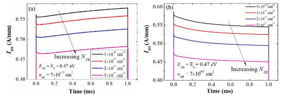
Figure 36.
By varying buffer trap density, transient response of (a) gate lag and (b) drain lag are observed. Reproduced with permission [163]. Copyright 2021, Elsevier.
4.2.5. Kink Effect
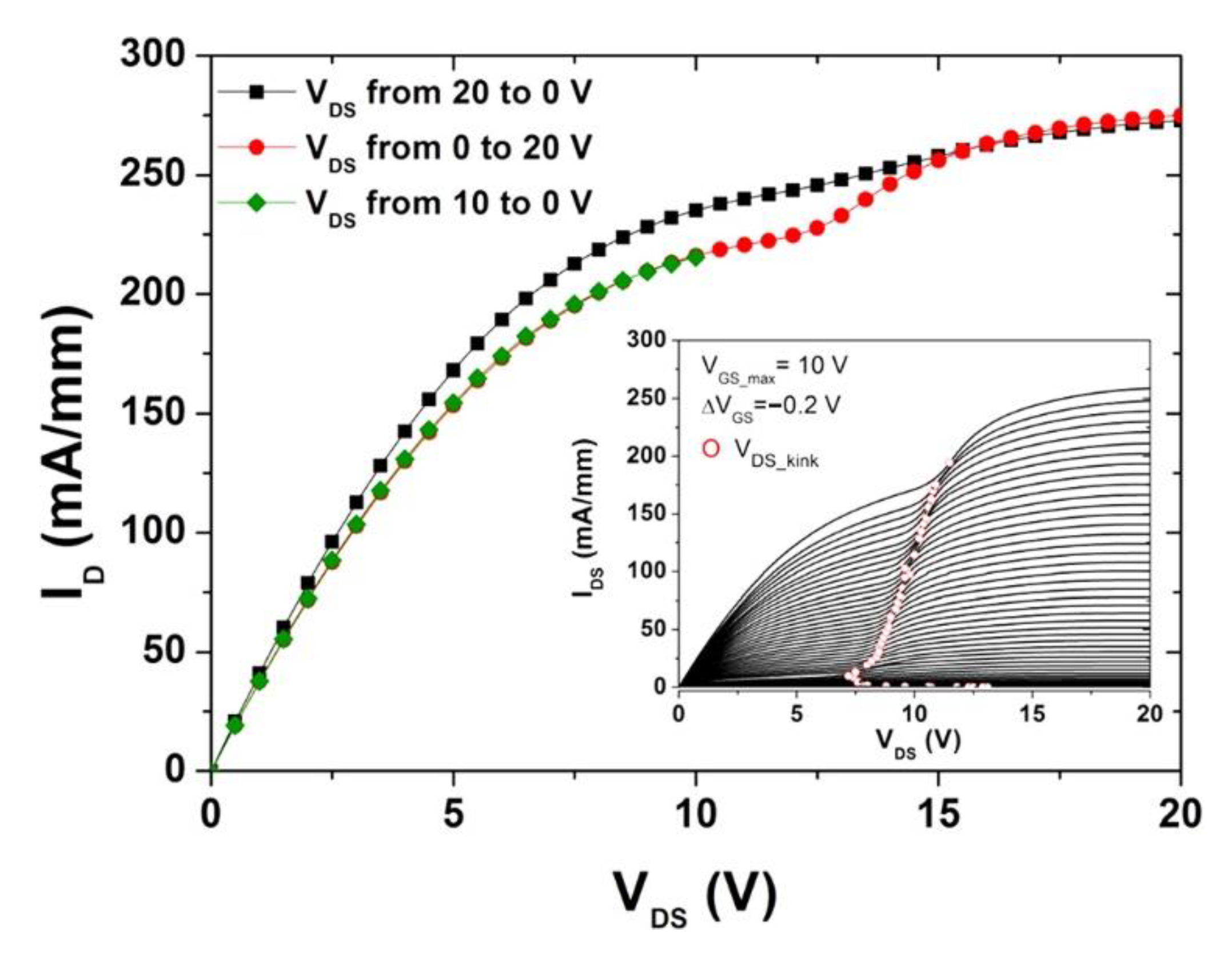
The kink effect refers to the output I–V characteristics of an undesirable change phenomenon caused by changes in the conductivity of the drain [164]. This is determined by the working point of the device, as well as the temperature, voltage, and current. As is evident in Figure 37, lengthy integration durations while comparing the output characteristics were achieved with a downward and upward VDS pumping. When the VDS is pushed down from a high value, the drain current drops at the VDS_kink position, but it reappears when the VDS is pumped up. As a result, the lower gd is due to trapping the states and is connected among the source and drain electric field. This is also supported by the fact that the magnitude of the kink is unaffected by the running VGS value, demonstrating that a large drain current is not required for a trap filling. The kink phenomenon has threshold characteristics related to the VDS_ kink. There is no kink in the IDS. if the VDS.max does not exceed the VDS_kink. As the gate voltage (VGS) is increased from 0 V to VGS.max, the nonmonotonic behavior of the VDS_kink is noticed. In the region of a relatively high VGS, the VDS_ kink rose with VGS. Nevertheless, the VDS_kink rose when VGS reduced in the near pinch-off zone. The inset figure demonstrates the nonmonotonic behavior of the kink voltage (VDS_kink) when the VGS is stepping from 10 V to 0 with ΔVGS =−0.2 V. Each sweep of VDS, is followed by a 5 min rest [165].
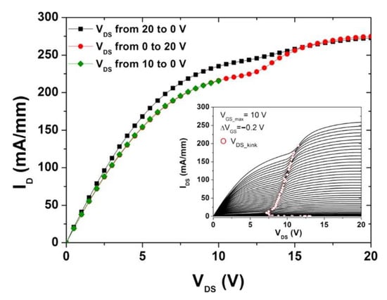
Figure 37.
The kink effect in the ID is clearly observed with a strong dependence on the VDS sweep direction. Reproduced with permission [165]. Copyright 2016, the author(s), published by the American Vacuum Society.
4.2.6. Runaway Effect
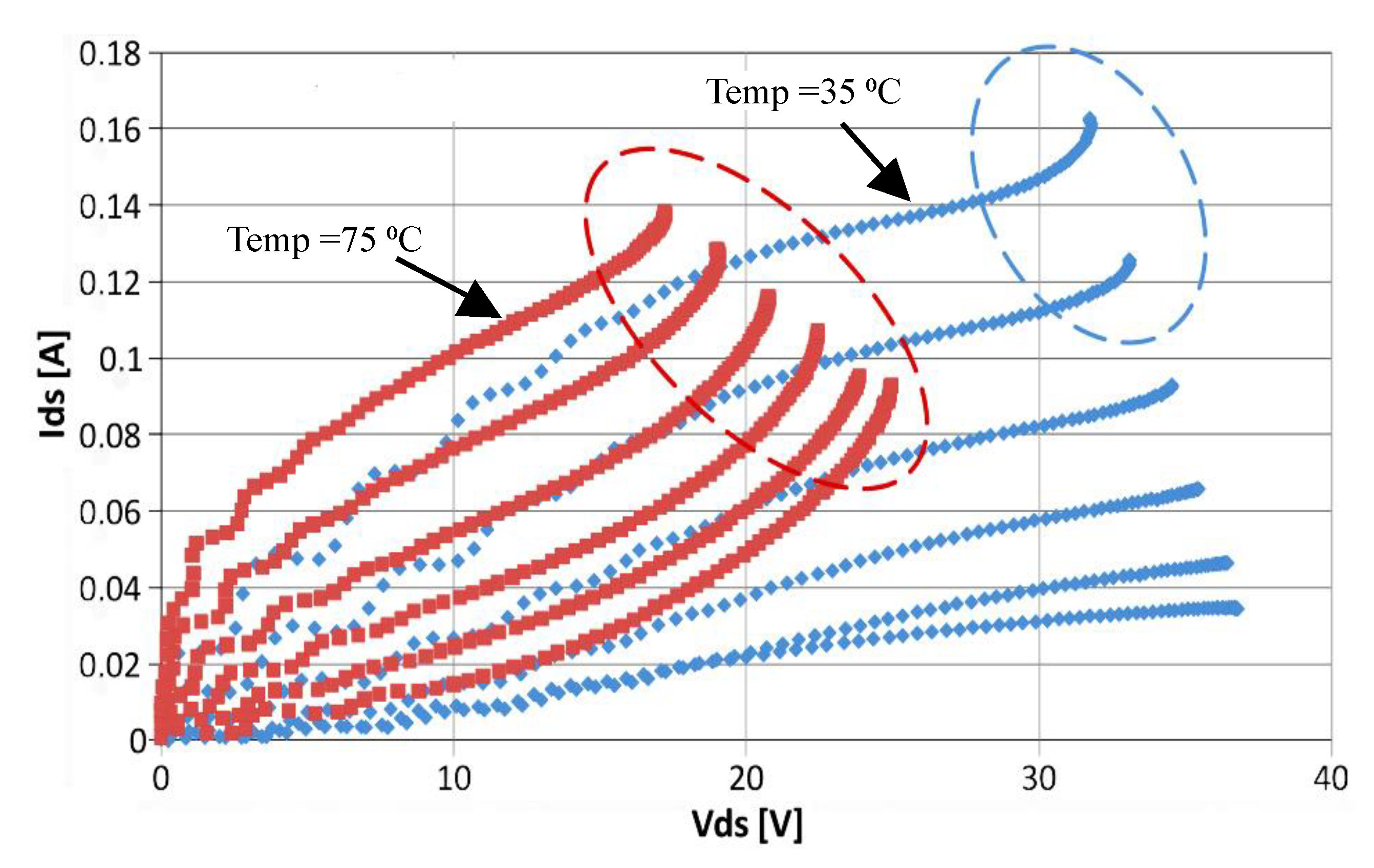
When the drain voltage is raised in the saturation regime, the runaway effect occurs, defined by a simultaneous increase in the drain and gate currents [166,167]. Usually, the gate-to-drain diode component dominates the gate leakage, which rises as the VDS approaches the threshold. The gate leakage is projected to decrease when the VGS is minimized. As shown in Figure 38, the absolute gate current in the runaway mode is larger for the lower VGS levels. After the runaway-inducing aging testing, the reliability characterizations might be severely detrimental since a continuous rise in the IG and ID could result in catastrophe failures, turning the runaway into an end-of-life mechanism. For the runaways, the significant drain and gate voltage will be noticed. Under open channel situations, the runaway shifts to a lower VDS and greater negative VG values. Lower activation voltages result from higher temperatures and longer aging durations. According to conduction mechanism research, the runaway seems to be linked to the Fowler–Nordheim tunnelling process.

Figure 38.
Output characteristics of the device reveal a runaway mechanism on the ellipse area with different temperatures. Reproduce with permission [167]. Copyright 2012, Elsevier.
4.2.7. Belly Shape Effect
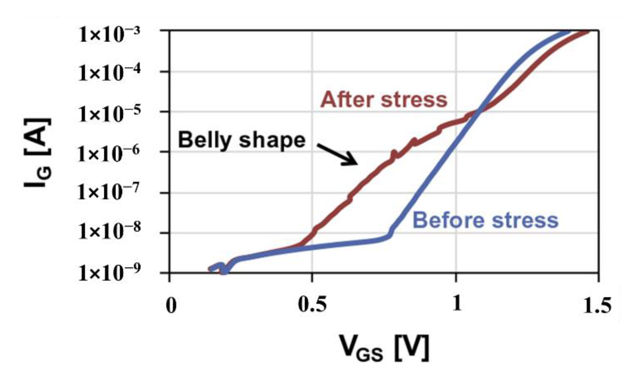
According to Brunel et al. [168], after the HTOL or HTRB reliability testing, the electrical parasitic phenomena known as the belly shape effect (BS) in which on the Schottky forward characteristic, an excess of the gate leakage current resembling a “belly shape” character is noticed [168,169]. Figure 39 shows a standard belly shape. After just a few hours of aging, a belly shape forms, with varying magnitudes during the aging process, indicating degradations due to variations in the epitaxial layers, metal, or surface states. Nonetheless, the mechanics of its development are still unknown, and additional research is needed to address the dependability manifestations. Without compromising the overall dependability, it may result in high leakage currents for fascinating research on the situation and internal physics.
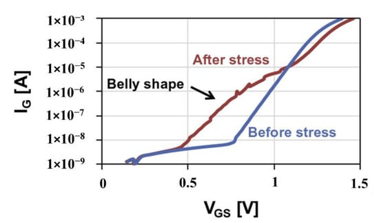
Figure 39.
Before (blue) and after (red) 4000 h of HTRB stress, the forward characteristics of an HEMT with BS are shown. Reproduced with permission [168]. Copyright 2013, Elsevier.
4.3. Breakdown Voltage in GaN HEMTs Device
Gallium nitride transistors are expected to play an essential role in the next-generation power converters, thanks to the high expected breakdown voltage, which is a direct consequence of the high breakdown field of GaN (>300 V/µm). Thus, in switching the operation, the transistors alternate between the on-state, where the gate opens the channel and allows the carriers to flow through the device, and the off-state, where the gate closes the channel and blocks the carriers’ current. At the off-state, the gate potential, VGS, is lower than the device’s threshold voltage, VTH, and is considered a subthreshold condition. For an efficient switching, the off-state operation point conditions should be at a high positive drain voltage and negligible drain current; therefore, a strong gate-blocking capability is required. At very high positive drain voltage conditions, the blocking capability of the device degrades and gives rise to the subthreshold leakage (STL) current. The subthreshold leakage current will increase and become significant, thereby reducing the efficiency of the switching. A significant leakage current is three orders of magnitude lower than the device’s maximal output current. At high voltages, currents higher than this value may initiate destructive processes in the device; therefore, it is considered the starting point of the device breakdown. In most cases, the breakdown voltage is either the sub-threshold drain leakage, or the gate leakage increases above 1 mA/mm.
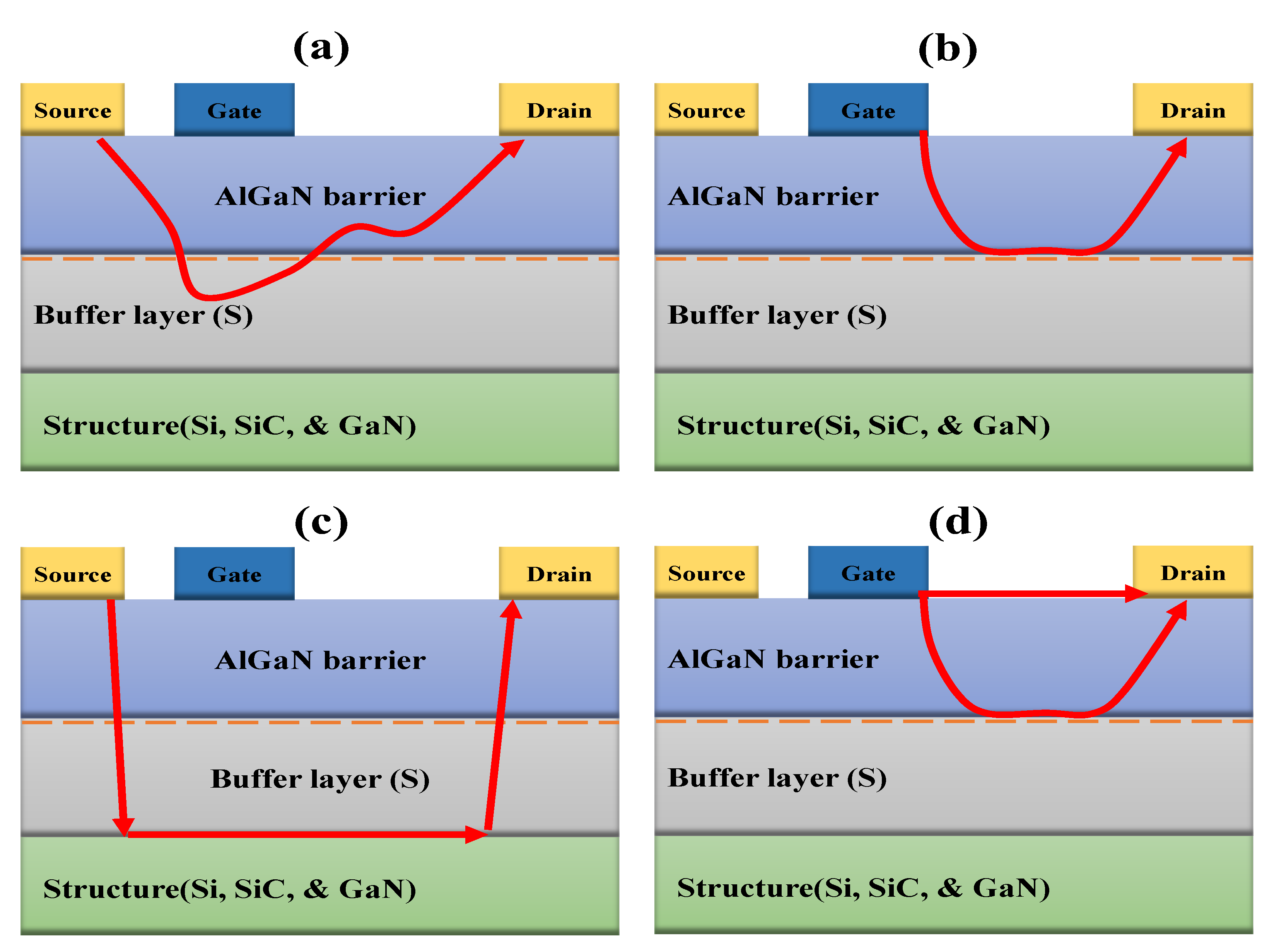
The main physical reasons for sub-threshold current leakages (STL) increased at a higher drain bias voltage are sketched in Figure 40. The STL has to be taken into account for a high voltage GaN device engineering and it is explained as follows:
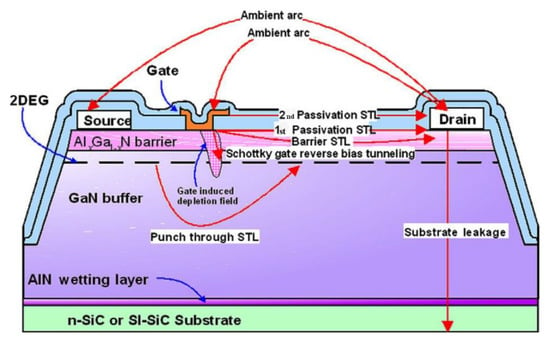
Figure 40.
Illustration of most important sub-threshold current leakages (STL) and breakdown paths might appear during high voltage in GaN-based HEMTs. Reproduced with permission [170]. Copyright 2011, Elsevier.
First, the electrons punch through in the buffer underneath the gated channel region [171]: this effect depends on the magnitude of the vertical electric field in the gate region and the ability of the buffer structure to confine electrons to the channel, as shown in Figure 41a. Second, the Schottky gate reverses the bias tunnelling: this originates from the drain side edge of the gate and is triggered by the high electric fields present in this particular device region, as displayed in Figure 41b. Third, Figure 41c presents the vertical device breakdown or the substrate leakage across the epitaxial layers to the conductive substrates such as n-SiC or Si: this is mainly an issue of the buffering technology and can be prevented by suitable epitaxial concepts [171]. High-voltage GaN devices place very stringent demands on high-voltage buffer structures since, in most cases, these devices are fabricated on conductive substrates (Si, n-SiC) which are usually connected to either the drain or the source terminal of the power devices. Fourth, surface-related breakdown: this is mainly associated with the quality of device passivation, whether the interface is between the passivation layers or the semiconductor surface itself, as indicated in Figure 41d. Finally, an ambient arcing between the closely spaced device electrodes may also occur if the devices are operated in the air. Thus, this has to be taken into account by the device layout design, the technology, and design of the passivation, and also the device packaging.
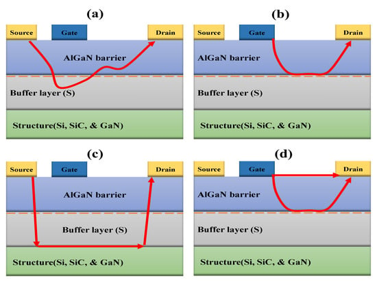
Figure 41.
Schematic represents the main source of limiting the high voltage capability of AlGaN/GaN HEMT on substrates (Si, SiC, or GaN). (a) Punch through effect, (b) Breakdown along channel region, (c) Breakdown through buffer layer, (d) Leakage currents originating from the gate structure.
5. Challenges for GaN HEMTs Device
Next-generation power-efficient converters might be created using GaN-based power devices if the fundamental problems pertaining to the material’s quality, device’s fabrication, and its performance can be resolved. However, challenges arise, such as it is impossible to crystallize GaN from melted material because the bulk GaN crystal development process is more challenging compared to Si and SiC. Bulk GaN substrates require high temperatures, >2200 °C, and a nitrogen pressure >6GPa, plus they have tough growth methods, such as a hydride vapor-phase epitaxy (HVPE), sodium flux, and an acidic/basic ammonothermal method is required. On top of that, these GaN substrates have a defect density of between 104 and 106/cm2, which necessitates a careful examination before they can be used for commercial purposes [172]. Ion implantation is used to dope the conventional Si and SiC power devices selectively. However, for GaN, it is still a highly complex process requiring specialized instruments capable of high-temperature (>1200 °C) and high-pressure conditions (>1 GPa) [173]. Bulk GaNs commercialization is hampered not only by the high cost and small size of these substrates, but also by the enormous initial investment required to set up GaN-specific fabs, which could drive up the average selling price (ASP) of discrete devices and further impede the adoption of these devices. Therefore, achieving significant advancements in both the cost and substrate size of these bulk GaN substrates is crucial.
Moreover, some other challenges, such as the GaN HEMT PAs, operate at high-frequency and high-power conditions, where the drain and the gate metals meltdown because of the Eddy current triggered by the magnetic field from the nearby coil. On the contrary, the high operating current may also facilitate the issue. The meltdown occurs at the Au layer, and several hints of Au can be traced in either subsequent layer [174]. The heavy ion irradiation makes the challenge for the GaN HEMT because this ion irradiation induces a device damage by creating lattice defects and accelerating the degradations of the GaN HEMT under tests (CGHV1J006D, manufactured by Wolfspeed, Durham, NC, USA). On the other hand, a gate injection triggers an impact ionization in the channel, thus inducing failures under the off-state. Its breakdown drain bias becomes lower than the pristine one, owing to the defect generations between the channel layer and the buffer layer during the ion irradiation [175].
Furthermore, after wet etches are done to remove the ohmic contacts of electrically stressed devices; the formation of nano-cracks underneath the ohmic metal contacts of GaN HEMTs becomes challenging for the researchers [176]. This crack might grow from the metal inclusions under the influence of a vertically oriented electric field, which introduces biaxial stress in the channel layer. The hoop stresses introduced by the biaxial compressive stresses and the residual tensile stress introduced in the epitaxial process impel the cracks to extend from the alloyed S–D contacts into the channel.
6. Conclusions
GaN HEMTs appear to be a competitive semiconductor technology for the foreseeable future. The existing and projected demand for GaN-based products in power industries is outlined. The benefits and physics of III-N materials are explained to comprehend GaN-based device transistors better. The contest between Si, GaN, SiC, and β-Ga2O3 is anticipated to heat up in the following years since these devices are forecast to represent a crucial function in the next generation of power converters. Research at both the academic and industry levels will lead to a significant advancement in device technology. On the other hand, reliability is still a big issue. Thus, the main GaN HEMT reliability concerns caused by the trap effects like a drain, a gate lag, a current collapse, and a breakdown voltage are explained briefly. Finally, we discussed the lateral type AlGaN/GaN HEMT devices, but in the future, we will include the vertical type AlGaN/GaN HEMT devices. Overall, the future growth of the GaN research field will be aided by the continued improvement of all these features, thanks to the more sophisticated machinery and higher-quality materials.
Author Contributions
Conceptualization, M.F.P.M., M.S. and H.K.; methodology, N.I.; software, N.I.; validation, H.K. and M.S.; formal analysis, M.F.P.M. and M.F.A.J.K.; investigation, N.I. and M.F.P.M.; resources, N.I. and M.F.P.M.; data curation, N.I., H.K. and M.F.P.M.; writing—original draft preparation, N.I.; writing—review and editing, N.I., S.F., M.S. and M.F.P.M.; visualization, N.I., S.F., M.S., M.F.A.J.K. and M.F.P.M.; supervision, S.F., M.S., M.F.A.J.K. and M.F.P.M.; project administration, M.F.P.M.; funding acquisition, S.F. and M.F.P.M. All authors have read and agreed to the published version of the manuscript.
Funding
This research was funded by Universiti Sains Malaysia’s Research University Incentive (RUI) grant “1001/PELECT/8014134”.
Data Availability Statement
Not applicable.
Acknowledgments
The author would like to express his gratitude to USMs School of Electrical and Electronic Engineering, CEDEC, and INOR for providing the research facilities.
Conflicts of Interest
The authors declare no conflict of interest.
References
- Fewson, D. Introduction to Power Electronics; Butterworth-Heinemann: Oxford, UK, 1998. [Google Scholar]
- Baliga, B.J. 1—Introduction. In Wide Bandgap Semiconductor Power Devices; Baliga, B.J., Ed.; Woodhead Publishing: Sawston, UK, 2019; pp. 1–19. [Google Scholar] [CrossRef]
- Mishra, U.K.; Parikh, P.; Wu, Y.-F. AlGaN/GaN HEMTs-an overview of device operation and applications. Proc. IEEE 2002, 90, 1022–1031. [Google Scholar] [CrossRef]
- Power GaN 2021: Epitaxy, Devices, Application and Technology Trends Report. 2021. Available online: http://www.yole.fr/GaN_Power_Epitaxy_Devices_Applications_Technology_Trends_2021.aspx (accessed on 1 May 2021).
- Compound Semiconductor Quarterly Market Monitor: Q3-2020. 2020. Available online: https://www.i-micronews.com/improved-reliability-in-power-gan-will-further-drive-its-market-growth-an-interview-with-transphorm/?cn-reloaded=1 (accessed on 5 November 2020).
- RF GaN 2021: Applications, Players, Technology and Substrates 2021 Report. 2021. Available online: https://s3.i-micronews.com/uploads/2021/06/YINTR21191-GaN_RF_Market_June_2021_Yole_Flyer.pdf (accessed on 1 June 2021).
- Millan, J.; Godignon, P.; Perpiñà, X.; Pérez-Tomás, A.; Rebollo, J. A survey of wide bandgap power semiconductor devices. IEEE Trans. Power Electron. 2013, 29, 2155–2163. [Google Scholar] [CrossRef]
- Hudgins, J.L.; Simin, G.S.; Santi, E.; Khan, M.A. An assessment of wide bandgap semiconductors for power devices. IEEE Trans. Power Electron. 2003, 18, 907–914. [Google Scholar] [CrossRef]
- Milligan, J.; Sheppard, S.; Pribble, W.; Wu, Y.-F.; Muller, G.; Palmour, J. SiC and GaN wide bandgap device technology overview. In Proceedings of the 2007 IEEE Radar Conference, Waltham, MA, USA, 17–20 April 2007; pp. 960–964. [Google Scholar]
- Devices, P.G. Materials, Applications and Reliability; Springer International Publishing: Cham, Switzerland, 2017. [Google Scholar]
- Schweber, B. Use SiC-Based MOSFETs to Improve Power Conversion Efficiency; Digi-Key Electronics: Thief River Falls, MN, USA, 2019. [Google Scholar]
- Ballestín-Fuertes, J.; Muñoz-Cruzado-Alba, J.; Sanz-Osorio, J.F.; Laporta-Puyal, E. Role of Wide Bandgap Materials in Power Electronics for Smart Grids Applications. Electronics 2021, 10, 677. [Google Scholar] [CrossRef]
- Marino, F.; Faralli, N.; Ferry, D.; Goodnick, S.; Saraniti, M. Figures of merit in high-frequency and high-power GaN HEMTs. J. Phys. Conf. Ser. 2009, 193, 012040. [Google Scholar] [CrossRef]
- Baliga, B.J. Power semiconductor device figure of merit for high-frequency applications. IEEE Electron Device Lett. 1989, 10, 455–457. [Google Scholar] [CrossRef]
- Shur, M.; Davis, R.F. GaN-Based Materials and Devices: Growth, Fabrication, Characterization and Performance; World Scientific: Toh Tuck, Singapore, 2004; Volume 33. [Google Scholar]
- Nikolaev, V.I.; Stepanov, S.I.; Romanov, A.E.; Bougrov, V.E. 14–Gallium oxide. In Single Crystals of Electronic Materials; Fornari, R., Ed.; Woodhead Publishing: Sawston, UK, 2019; pp. 487–521. [Google Scholar] [CrossRef]
- Bernardini, F.; Fiorentini, V.; Vanderbilt, D. Accurate calculation of polarization-related quantities in semiconductors. Phys. Rev. B 2001, 63, 193201. [Google Scholar] [CrossRef]
- Rais-Zadeh, M.; Gokhale, V.J.; Ansari, A.; Faucher, M.; Théron, D.; Cordier, Y.; Buchaillot, L.J. Gallium nitride as an electromechanical material. J. Microelectromech. Syst. 2014, 23, 1252–1271. [Google Scholar] [CrossRef]
- Bernardini, F.; Fiorentini, V.; Vanderbilt, D. Spontaneous polarization and piezoelectric constants of III-V nitrides. Phys. Rev. B 1997, 56, R10024. [Google Scholar] [CrossRef]
- Asbeck, P.M. Electronic properties of III-nitride materials and basics of III-nitride FETs. In Semiconductors and Semimetals; Elsevier: Amsterdam, The Netherlands, 2019; Volume 102, pp. 1–40. [Google Scholar]
- Ambacher, O.; Majewski, J.; Miskys, C.; Link, A.; Hermann, M.; Eickhoff, M.; Stutzmann, M.; Bernardini, F.; Fiorentini, V.; Tilak, V.J. Pyroelectric properties of Al (In) GaN/GaN hetero-and quantum well structures. J. Phys. Condens. Matter 2002, 14, 3399. [Google Scholar] [CrossRef]
- Pearton, S.; Zolper, J.; Shul, R.; Ren, F.J. GaN: Processing, defects, and devices. J. Appl. Phys. 1999, 86, 1–78. [Google Scholar] [CrossRef]
- Ambacher, O.; Foutz, B.; Smart, J.; Shealy, J.; Weimann, N.; Chu, K.; Murphy, M.; Sierakowski, A.; Schaff, W.; Eastman, L.J. Two dimensional electron gases induced by spontaneous and piezoelectric polarization in undoped and doped AlGaN/GaN heterostructures. J. Appl. Phys. 2000, 87, 334–344. [Google Scholar] [CrossRef]
- Cros, A.; Garro, N.; Cantarero, A.; Coraux, J.; Renevier, H.; Daudin, B. Raman scattering as a tool for the evaluation of strain in Ga N/Al N quantum dots: The effect of capping. Phys. Rev. B 2007, 76, 165403. [Google Scholar] [CrossRef]
- Pearton, S.; Ren, F.; Zhang, A.; Lee, K.; Reports, E.R. Fabrication and performance of GaN electronic devices. Mater. Sci. Eng. R Rep. 2000, 30, 55–212. [Google Scholar] [CrossRef]
- Grabowski, S.P.; Schneider, M.; Nienhaus, H.; Mönch, W.; Dimitrov, R.; Ambacher, O.; Stutzmann, M. Electron affinity of AlxGa1−xN(0001) surfaces. Appl. Phys. Lett. 2001, 78, 2503–2505. [Google Scholar] [CrossRef]
- Dabiran, A.M.; Wowchak, A.M.; Osinsky, A.; Xie, J.; Hertog, B.; Cui, B.; Look, D.C.; Chow, P.P. Very high channel conductivity in low-defect AlN/GaN high electron mobility transistor structures. Appl. Phys. Lett. 2008, 93, 082111. [Google Scholar] [CrossRef]
- Kuzmik, J.; Pozzovivo, G.; Ostermaier, C.; Strasser, G.; Pogany, D.; Gornik, E.; Carlin, J.-F.; Gonschorek, M.; Feltin, E.; Grandjean, N. Analysis of degradation mechanisms in lattice-matched InAlN/GaN high-electron-mobility transistors. J. Appl. Phys. 2009, 106, 124503. [Google Scholar] [CrossRef]
- Lee, S.R.; Wright, A.F.; Crawford, M.H.; Petersen, G.A.; Han, J.; Biefeld, R.M. The band-gap bowing of AlxGa1−xN alloys. Appl. Phys. Lett. 1999, 74, 3344–3346. [Google Scholar] [CrossRef]
- Palacios, T.; Mishra, U.K. AlGaN/GaN High Electron Mobility Transistors. In Nitride Semiconductor Devices: Principles and Simulation; John Wiley & Sons: Hoboken, NJ, USA, 2007; pp. 211–233. [Google Scholar] [CrossRef]
- He, X.-G.; Zhao, D.-G.; Jiang, D.-S. Formation of two-dimensional electron gas at AlGaN/GaN heterostructure and the derivation of its sheet density expression. Chin. Phys. B 2015, 24, 067301. [Google Scholar] [CrossRef]
- Jones, E.A.; Wang, F.F.; Costinett, D. Review of Commercial GaN Power Devices and GaN-Based Converter Design Challenges. IEEE J. Emerg. Sel. Top. Power Electron. 2016, 4, 707–719. [Google Scholar] [CrossRef]
- Khan, M.A.; Bhattarai, A.; Kuznia, J.N.; Olson, D.T. High electron mobility transistor based on a GaN-AlxGa1−xN heterojunction. Appl. Phys. Lett. 1993, 63, 1214–1215. [Google Scholar] [CrossRef]
- Ueda, H.; Sugimoto, M.; Uesugi, T.; Fujishima, O.; Kachi, T. High current operation of GaN power HEMT. In Proceedings of the ISPSD’05 17th International Symposium on Power Semiconductor Devices and Ics, Santa Barbara, CA, USA, 23–26 May 2005; pp. 311–314. [Google Scholar]
- Schwierz, F.; Ambacher, O. Recent advances in GaN HEMT development. In Proceedings of the 11th IEEE International Symposium on Electron Devices for Microwave and Optoelectronic Applications EDMO 2003, Orlando, FL, USA, 17–18 November 2003; pp. 204–209. [Google Scholar]
- Amano, H.; Baines, Y.; Beam, E.; Borga, M.; Bouchet, T.; Chalker, P.R.; Charles, M.; Chen, K.J.; Chowdhury, N.; Chu, R.J. The 2018 GaN power electronics roadmap. J. Phys. D Appl. Phys. 2018, 51, 163001. [Google Scholar] [CrossRef]
- Zhang, J.; Hao, Y.; Zhang, J.; Ni, J. The mobility of two-dimensional electron gas in AlGaN/GaN heterostructures with varied Al content. Sci. China Ser. F Inf. Sci. 2008, 51, 780–789. [Google Scholar] [CrossRef]
- Miyoshi, M.; Egawa, T.; Ishikawa, H. Structural characterization of strained AlGaN layers in different Al content AlGaN/GaN heterostructures and its effect on two-dimensional electron transport properties. J. Vac. Sci. Technol. B 2005, 23, 1527–1531. [Google Scholar] [CrossRef]
- Jones, E.A.; Wang, F.; Ozpineci, B. Application-based review of GaN HFETs. In Proceedings of the 2014 IEEE Workshop on Wide Bandgap Power Devices and Applications, Knoxville, TN, USA, 13–15 October 2014; pp. 24–29. [Google Scholar]
- Derluyn, J.; Boeykens, S.; Cheng, K.; Vandersmissen, R.; Das, J.; Ruythooren, W.; Degroote, S.; Leys, M.; Germain, M.; Borghs, G.J. Improvement of AlGaN/GaN high electron mobility transistor structures by in situ deposition of a Si3N4 surface layer. J. Appl. Phys. 2005, 98, 054501. [Google Scholar] [CrossRef]
- Hua, M.; Liu, C.; Yang, S.; Liu, S.; Fu, K.; Dong, Z.; Cai, Y.; Zhang, B.; Chen, K.J. GaN-based metal-insulator-semiconductor high-electron-mobility transistors using low-pressure chemical vapor deposition SiN x as gate dielectric. IEEE Electron Device Lett. 2015, 36, 448–450. [Google Scholar] [CrossRef]
- Hashizume, T.; Nishiguchi, K.; Kaneki, S.; Kuzmik, J.; Yatabe, Z. State of the art on gate insulation and surface passivation for GaN-based power HEMTs. Mater. Sci. Semicond. Process. 2018, 78, 85–95. [Google Scholar] [CrossRef]
- Sze, S.M.; Li, Y.; Ng, K.K. Physics of Semiconductor Devices; John Wiley & Sons: Hoboken, NJ, USA, 2021. [Google Scholar]
- Asgari, A.; Kalafi, M. The control of two-dimensional-electron-gas density and mobility in AlGaN/GaN heterostructures with Schottky gate. Mater. Sci. Eng. C 2006, 26, 898–901. [Google Scholar] [CrossRef]
- Ren, J.; Tang, C.W.; Feng, H.; Jiang, H.; Yang, W.; Zhou, X.; Lau, K.M.; Sin, J.K. A novel 700 V monolithically integrated Si-GaN ‘ascaded field effect transistor. IEEE Electron Device Lett. 2018, 39, 394–396. [Google Scholar] [CrossRef]
- Xue, P.; Maresca, L.; Riccio, M.; Breglio, G.; Irace, A. Experimental study on the short-circuit instability of cascode GaN HEMTs. IEEE Trans. Electron Devices 2020, 67, 1686–1692. [Google Scholar] [CrossRef]
- Wu, C.-C.; Jeng, S.-L. Comparison of Parasitic Capacitances of Packaged Cascode Gallium Nitride Field-effect Transistors. Sens. Mater. 2018, 30, 453–461. [Google Scholar]
- Elangovan, S.; Cheng, S.; Chang, E.Y. Reliability characterization of gallium nitride MIS-HEMT based cascode devices for power electronic applications. Energies 2020, 13, 2628. [Google Scholar] [CrossRef]
- Lidow, A.; Strydom, J.; de Rooij, M.; Reusch, D. GaN Transistors for Efficient Power Conversion; Wiley: Hoboken, NJ, USA, 2014. [Google Scholar]
- Cai, Y.; Zhou, Y.; Chen, K.J.; Lau, K.M. High-performance enhancement-mode AlGaN/GaN HEMTs using fluoride-based plasma treatment. IEEE Electron Device Lett. 2005, 26, 435–437. [Google Scholar]
- Khan, M.A.; Chen, Q.; Sun, C.; Yang, J.; Blasingame, M.; Shur, M.; Park, H. Enhancement and depletion mode GaN/AlGaN heterostructure field effect transistors. Appl. Phys. Lett. 1996, 68, 514–516. [Google Scholar] [CrossRef]
- Huang, S.; Wang, X.; Liu, X.; Wang, Y.; Fan, J.; Yang, S.; Yin, H.; Wei, K.; Wang, W.; Gao, H. Monolithic integration of E/D-mode GaN MIS-HEMTs on ultrathin-barrier AlGaN/GaN heterostructure on Si substrates. Appl. Phys. Express 2019, 12, 024001. [Google Scholar] [CrossRef]
- Cai, Y.; Zhou, Y.; Lau, K.M.; Chen, K.J. Control of threshold voltage of AlGaN/GaN HEMTs by fluoride-based plasma treatment: From depletion mode to enhancement mode. IEEE Trans. Electron Devices 2006, 53, 2207–2215. [Google Scholar] [CrossRef]
- Tang, X.; Li, B.K.; Moghadam, H.A.; Tanner, P.; Han, J.S.; Dimitrijev, S. Mechanism of Threshold Voltage Shift in p-GaN Gate AlGaN/GaN Transistors. IEEE Electron Device Lett. 2018, 39, 1145–1148. [Google Scholar] [CrossRef]
- Uemoto, Y.; Hikita, M.; Ueno, H.; Matsuo, H.; Ishida, H.; Yanagihara, M.; Ueda, T.; Tanaka, T.; Ueda, D. Gate injection transistor (GIT)—A normally-off AlGaN/GaN power transistor using conductivity modulation. IEEE Trans. Electron Devices 2007, 54, 3393–3399. [Google Scholar] [CrossRef]
- Jubadi, W.; Packeer, F.; Missous, M. Optimization of Empirical Modelling of Advanced Highly Strained In 0.7 Ga 0.3 As/In 0.52 Al 0.48 As pHEMTs for Low Noise Amplifier. Int. J. Electr. Comput. Eng. 2017, 7, 3393–3399. [Google Scholar]
- Greco, G.; Iucolano, F.; Roccaforte, F. Review of technology for normally-off HEMTs with p-GaN gate. Mater. Sci. Semicond. Process. 2018, 78, 96–106. [Google Scholar] [CrossRef]
- Roccaforte, F.; Greco, G.; Fiorenza, P.; Iucolano, F. An overview of normally-off GaN-based high electron mobility transistors. Materials 2019, 12, 1599. [Google Scholar] [CrossRef] [PubMed]
- Hilt, O.; Knauer, A.; Brunner, F.; Bahat-Treidel, E.; Würfl, J. Normally-off AlGaN/GaN HFET with p-type Ga Gate and AlGaN buffer. In Proceedings of the 2010 22nd International Symposium on Power Semiconductor Devices & IC’s (ISPSD), Hiroshima, Japan, 6–10 June 2010; pp. 347–350. [Google Scholar]
- Meneghini, M.; Hilt, O.; Wuerfl, J.; Meneghesso, G. Technology and reliability of normally-off GaN HEMTs with p-type gate. Energies 2017, 10, 153. [Google Scholar] [CrossRef]
- Efthymiou, L.; Longobardi, G.; Camuso, G.; Chien, T.; Chen, M.; Udrea, F. On the physical operation and optimization of the p-GaN gate in normally-off GaN HEMT devices. Appl. Phys. Lett. 2017, 110, 123502. [Google Scholar] [CrossRef]
- Posthuma, N.; You, S.; Liang, H.; Ronchi, N.; Kang, X.; Wellekens, D.; Saripalli, Y.; Decoutere, S. Impact of Mg out-diffusion and activation on the p-GaN gate HEMT device performance. In Proceedings of the 2016 28th International Symposium on Power Semiconductor Devices and ICs (ISPSD), Žofín Palace, Prague, Czech Republic, 12–16 June 2016; pp. 95–98. [Google Scholar]
- Islam, N.; Yusof, N.S.; Mohamed, M.F.P.; Syamsul, M.; Khan, M.F.A.J.; Ghazali, N.A.; Hairi, M.H. Optimization of 1-µm gate length InGaAs-InAlAs pHEMT. Microelectron. Int. 2022. [Google Scholar] [CrossRef]
- Kinoshita, T.; Obata, T.; Yanagi, H.; Inoue, S.-I. High p-type conduction in high-Al content Mg-doped AlGaN. Appl. Phys. Lett. 2013, 102, 012105. [Google Scholar] [CrossRef]
- Roccaforte, F.; Frazzetto, A.; Greco, G.; Giannazzo, F.; Fiorenza, P.; Nigro, R.L.; Saggio, M.; Leszczyński, M.; Pristawko, P.; Raineri, V. Critical issues for interfaces to p-type SiC and GaN in power devices. Appl. Surf. Sci. 2012, 258, 8324–8333. [Google Scholar] [CrossRef]
- Callsen, G.; Wagner, M.; Kure, T.; Reparaz, J.; Bügler, M.; Brunnmeier, J.; Nenstiel, C.; Hoffmann, A.; Hoffmann, M.; Tweedie, J. Optical signature of Mg-doped GaN: Transfer processes. Phys. Rev. B 2012, 86, 075207. [Google Scholar] [CrossRef]
- Packeer, F.; Mohamad Isa, M.; Mat Jubadi, W.; Ian, K.W.; Missous, M. Fabrication and characterization of tensile In0.3Al0.7As barrier and compressive In0.7Ga0.3 As channel pHEMTs having extremely low gate leakage for low-noise applications. J. Phys. D Appl. Phys. 2013, 46, 264002. [Google Scholar] [CrossRef]
- Kaneko, S.; Kuroda, M.; Yanagihara, M.; Ikoshi, A.; Okita, H.; Morita, T.; Tanaka, K.; Hikita, M.; Uemoto, Y.; Takahashi, S. Current-collapse-free operations up to 850 V by GaN-GIT utilizing hole injection from drain. In Proceedings of the 2015 IEEE 27th International Symposium on Power Semiconductor Devices & IC’s (ISPSD), Hong Kong, China, 10–14 May 2015; pp. 41–44. [Google Scholar]
- Sayadi, L.; Iannaccone, G.; Sicre, S.; Häberlen, O.; Curatola, G. Threshold voltage instability in p-GaN gate AlGaN/GaN HFETs. IEEE Trans. Electron Devices 2018, 65, 2454–2460. [Google Scholar] [CrossRef]
- Packeer Mohamed, M.F.; Mohamed Omar, M.F.; Akbar Jalaludin Khan, M.F.; Ghazali, N.A.; Hairi, M.H.; Falina, S.; Samsol Baharin, M.S.N. New Submicron Low Gate Leakage In0.52Al0.48As-In0.7Ga0.3As pHEMT for Low-Noise Applications. Micromachines 2021, 12, 1497. [Google Scholar] [CrossRef]
- Zhou, G.; Wan, Z.; Yang, G.; Jiang, Y.; Sokolovskij, R.; Yu, H.; Xia, G. Gate leakage suppression and breakdown voltage enhancement in p-GaN HEMTs using metal/graphene gates. IEEE Trans. Electron Devices 2020, 67, 875–880. [Google Scholar] [CrossRef]
- Chiu, H.-C.; Liu, C.-H.; Huang, C.-R.; Chiu, C.-C.; Wang, H.-C.; Kao, H.-L.; Lin, S.-Y.; Chien, F.-T. Normally-Off p-GaN Gated AlGaN/GaN MIS-HEMTs with ALD-Grown Al2O3/AlN Composite Gate Insulator. Membranes 2021, 11, 727. [Google Scholar] [CrossRef]
- Ngo, T.H.; Comyn, R.; Chenot, S.; Brault, J.; Damilano, B.; Vezian, S.; Frayssinet, E.; Cozette, F.; Defrance, N.; Lecourt, F. Combination of selective area sublimation of p-GaN and regrowth of AlGaN for the co-integration of enhancement mode and depletion mode high electron mobility transistors. Solid-State Electron. 2022, 188, 108210. [Google Scholar] [CrossRef]
- Xu, N.; Hao, R.; Chen, F.; Zhang, X.; Zhang, H.; Zhang, P.; Ding, X.; Song, L.; Yu, G.; Cheng, K. Gate leakage mechanisms in normally off p-GaN/AlGaN/GaN high electron mobility transistors. Appl. Phys. Lett. 2018, 113, 152104. [Google Scholar] [CrossRef]
- Zhang, W.; Liu, X.; Fu, L.; Huang, R.; Zhao, S.; Zhang, J.; Zhang, J.; Hao, Y. Investigation of normally-off GaN-based p-channel and n-channel heterojunction field-effect transistors for monolithic integration. Results Phys. 2021, 24, 104209. [Google Scholar] [CrossRef]
- Chiu, H.-C.; Chang, Y.-S.; Li, B.-H.; Wang, H.-C.; Kao, H.-L.; Hu, C.-W.; Xuan, R. High-performance normally off p-GaN gate HEMT with composite AlN/Al 0.17 Ga 0.83 N/Al 0.3 Ga 0.7 N barrier layers design. IEEE J. Electron Devices Soc. 2018, 6, 201–206. [Google Scholar] [CrossRef]
- Su, S.; Zhong, Y.; Zhou, Y.; Gao, H.; Zhan, X.; Chen, X.; Guo, X.; Sun, Q.; Zhang, Z.; Bi, W. A p-GaN-Gated Hybrid Anode Lateral Diode with a Thicker AlGaN Barrier Layer. Phys. Status Solidi 2020, 217, 1900781. [Google Scholar] [CrossRef]
- Wang, H.-C.; Liu, C.-H.; Huang, C.-R.; Chiu, H.-C.; Kao, H.-L.; Liu, X. Hole Injection Effect and Dynamic Characteristic Analysis of Normally Off p-GaN HEMT with AlGaN Cap Layer on Low-Resistivity SiC Substrate. Micromachines 2022, 13, 807. [Google Scholar] [CrossRef]
- Sun, C.; Hao, R.; Xu, N.; He, T.; Shi, F.; Yu, G.; Song, L.; Huang, Z.; Huang, R.; Zhao, Y. Normally-off p-GaN/AlGaN/GaN high-electron-mobility transistors using oxygen plasma treatment. Appl. Phys. Express 2019, 12, 051001. [Google Scholar] [CrossRef]
- Chang, Y.-C.; Ho, Y.-L.; Huang, T.-Y.; Huang, D.-W.; Wu, C.-H. Investigation of Normally-Off p-GaN/AlGaN/GaN HEMTs Using a Self-Terminating Etching Technique with Multi-Finger Architecture Modulation for High Power Application. Micromachines 2021, 12, 432. [Google Scholar] [CrossRef]
- Zhou, G.; Zeng, F.; Gao, R.; Wang, Q.; Cheng, K.; Li, L.; Xiang, P.; Du, F.; Xia, G.; Yu, H. p-GaN Gate HEMTs With 10.6 V Maximum Gate Drive Voltages by Mg Doping Engineering. IEEE Trans. Electron Devices 2022, 69, 2282–2286. [Google Scholar] [CrossRef]
- Taube, A.; Kamiński, M.; Ekielski, M.; Kruszka, R.; Jankowska-Śliwińska, J.; Michałowski, P.P.; Zdunek, J.; Szerling, A. Selective etching of p-GaN over Al0.25Ga0.75N in Cl2/Ar/O2 ICP plasma for fabrication of normally-off GaN HEMTs. Mater. Sci. Semicond. Process. 2021, 122, 105450. [Google Scholar] [CrossRef]
- Wang, H.; Mao, W.; Zhao, S.; He, Y.; Chen, J.; Du, M.; Zheng, X.; Wang, C.; Zhang, C.; Zhang, J. Unidirectional p-GaN gate HEMT with composite source-drain field plates. Sci. China Inf. Sci. 2022, 65, 129405. [Google Scholar] [CrossRef]
- Zhong, Y.; Su, S.; Chen, X.; Zhou, Y.; He, J.; Gao, H.; Zhan, X.; Guo, X.; Liu, J.; Sun, Q.; et al. Normally-off HEMTs With Regrown p-GaN Gate and Low-Pressure Chemical Vapor Deposition SiNx Passivation by Using an AlN Pre-Layer. IEEE Electron Device Lett. 2019, 40, 1495–1498. [Google Scholar] [CrossRef]
- Lükens, G.; Hahn, H.; Kalisch, H.; Vescan, A. Self-Aligned Process for Selectively Etched p-GaN-Gated AlGaN/GaN-on-Si HFETs. IEEE Trans. Electron Devices 2018, 65, 3732–3738. [Google Scholar] [CrossRef]
- Wang, H.; Mao, W.; Zhao, S.; Chen, J.; Du, M.; Zheng, X.; Wang, C.; Zhang, C.; Zhang, J.; Hao, Y. Reverse blocking p-GaN gate AlGaN/GaN HEMTs with hybrid p-GaN ohmic drain. Superlattices Microstruct. 2021, 156, 106931. [Google Scholar] [CrossRef]
- Huang, Y.-C.; Chiu, H.-C.; Kao, H.-L.; Wang, H.-C.; Liu, C.-H.; Huang, C.-R.; Chen, S.-W. High Thermal Dissipation of Normally off p-GaN Gate AlGaN/GaN HEMTs on 6-Inch N-Doped Low-Resistivity SiC Substrate. Micromachines 2021, 12, 509. [Google Scholar] [CrossRef]
- Liu, K.; Wang, R.; Wang, C.; Zheng, X.; Ma, X.-h.; Bai, J.; Cheng, B.; Liu, R.; Li, A.; Zhao, Y.; et al. The influence of lightly-doped p-GaN cap layer on p-GaN/AlGaN/GaN HEMT. Semicond. Sci. Technol. 2022, 37, 075005. [Google Scholar] [CrossRef]
- Rolland, G.; Rodriguez, C.; Gommé, G.; Boucherif, A.; Chakroun, A.; Bouchilaoun, M.; Pepin, M.C.; El Hamidi, F.; Maher, S.; Arès, R.; et al. High Power Normally-OFF GaN/AlGaN HEMT with Regrown p Type GaN. Energies 2021, 14, 6098. [Google Scholar] [CrossRef]
- Kumar, V.; Kuliev, A.; Tanaka, T.; Otoki, Y.; Adesida, I. High transconductance enhancement-mode AlGaN/GaN HEMTs on SiC substrate. In Electronics Letters; Institution of Engineering and Technology: Stevenage, UK, 2003; Volume 39, pp. 1758–1760. [Google Scholar]
- Pu, T.F. Study on Normally-off AlGaN/GaN Heterostructure Field-Effect Transistors with P-GaN Cap Layer. Ph.D. Thesis, Tokushima University, Tokushima, Japan, 2019. [Google Scholar]
- Hu, Q.; Li, S.; Li, T.; Wang, X.; Li, X.; Wu, Y. Channel Engineering of Normally-OFF AlGaN/GaN MOS-HEMTs by Atomic Layer Etching and HighHigh- κ Dielectric. IEEE Electron Device Lett. 2018, 39, 1377–1380. [Google Scholar] [CrossRef]
- He, Y.; Gao, H.; Wang, C.; Zhao, Y.; Lu, X.; Zhang, C.; Zheng, X.; Guo, L.; Ma, X.; Hao, Y. Comparative Study Between Partially and Fully Recessed-Gate Enhancement-Mode AlGaN/GaN MIS HEMT on the Breakdown Mechanism. Phys. Status Solidi 2019, 216, 1900115. [Google Scholar] [CrossRef]
- Zhang, J.; He, L.; Li, L.; Ni, Y.; Que, T.; Liu, Z.; Wang, W.; Zheng, J.; Huang, Y.; Chen, J.; et al. High-Mobility Normally OFF Al2O3/AlGaN/GaN MISFET With Damage-Free Recessed-Gate Structure. IEEE Electron Device Lett. 2018, 39, 1720–1723. Available online: https://digital-library.theiet.org/content/journals/10.1049/el_20031124 (accessed on 30 September 2018). [CrossRef]
- Fiorenza, P.; Greco, G.; Iucolano, F.; Patti, A.; Roccaforte, F. Channel Mobility in GaN Hybrid MOS-HEMT Using SiO2 as Gate Insulator. IEEE Trans. Electron Devices 2017, 64, 2893–2899. [Google Scholar] [CrossRef]
- He, J.; Cheng, W.C.; Wang, Q.; Cheng, K.; Yu, H.; Chai, Y. Recent Advances in GaN-Based Power HEMT Devices. Adv. Electron. Mater. 2021, 7, 2001045. [Google Scholar] [CrossRef]
- Hua, M.; Cai, X.; Yang, S.; Zhang, Z.; Zheng, Z.; Wang, N.; Chen, K.J. Enhanced Gate Reliability in GaN MIS-FETs by Converting the GaN Channel into Crystalline Gallium Oxynitride. ACS Appl. Electron. Mater. 2019, 1, 642–648. [Google Scholar] [CrossRef]
- Acurio, E.; Crupi, F.; Magnone, P.; Trojman, L.; Iucolano, F. Impact of AlN layer sandwiched between the GaN and the Al2O3 layers on the performance and reliability of recessed AlGaN/GaN MOS-HEMTs. Microelectron. Eng. 2017, 178, 42–47. [Google Scholar] [CrossRef]
- Wang, B.; Huang, W.; Chi, L.; Al-Hashimi, M.; Marks, T.J.; Facchetti, A. High-k Gate Dielectrics for Emerging Flexible and Stretchable Electronics. Chem. Rev. 2018, 118, 5690–5754. [Google Scholar] [CrossRef]
- Robertson, J.; Falabretti, B.J. Band offsets of high K gate oxides on III-V semiconductors. J. Appl. Phys. 2006, 100, 014111. [Google Scholar] [CrossRef]
- Reddy, B.P.K.; Teja, K.B.R.; Kandpal, K. Investigation on High-κ Dielectric for Low Leakage AlGaN/GaN MIS-HEMT Device, Using Material Selection Methodologies. Semiconductors 2018, 52, 420–430. [Google Scholar] [CrossRef]
- Khan, M.A.; Hu, X.; Sumin, G.; Lunev, A.; Yang, J.; Gaska, R.; Shur, M.S. AlGaN/GaN metal oxide semiconductor heterostructure field effect transistor. IEEE Electron Device Lett. 2000, 21, 63–65. [Google Scholar] [CrossRef]
- Eller, B.S.; Yang, J.; Nemanich, R.J. Electronic surface and dielectric interface states on GaN and AlGaN. J. Vac. Sci. Technol. A Vac. Surf. Film. 2013, 31, 050807. [Google Scholar] [CrossRef]
- Ochiai, M.; Akita, M.; Ohno, Y.; Kishimoto, S.; Maezawa, K.; Mizutani, T. AlGaN/GaN Heterostructure Metal-Insulator-Semiconductor High-Electron-Mobility Transistors with Si3N4 Gate Insulator. Jpn. J. Appl. Phys. 2003, 42, 2278–2280. [Google Scholar] [CrossRef]
- Lee, C.-T.; Chen, H.-W.; Lee, H.-Y. Metal–oxide–semiconductor devices using Ga2O3 dielectrics on n-type GaN. Appl. Phys. Lett. 2003, 82, 4304–4306. [Google Scholar] [CrossRef]
- Liu, S.; Yang, S.; Tang, Z.; Jiang, Q.; Liu, C.; Wang, M.; Chen, K.J. Al2O3/AlN/GaN MOS-Channel-HEMTs With an AlN Interfacial Layer. IEEE Electron Device Lett. 2014, 35, 723–725. [Google Scholar] [CrossRef]
- Huang, S.; Jiang, Q.; Yang, S.; Zhou, C.; Chen, K.J. Effective Passivation of AlGaN/GaN HEMTs by ALD-Grown AlN Thin Film. IEEE Electron Device Lett. 2012, 33, 516–518. [Google Scholar] [CrossRef]
- Hsu, C.-H.; Shih, W.-C.; Lin, Y.-C.; Hsu, H.-T.; Hsu, H.-H.; Huang, Y.-X.; Lin, T.-W.; Wu, C.-H.; Wu, W.-H.; Maa, J.-S.; et al. Improved linearity and reliability in GaN metal–oxide–semiconductor high-electron-mobility transistors using nanolaminate La2O3/SiO2 gate dielectric. Jpn. J. Appl. Phys. 2016, 55, 04EG04. [Google Scholar] [CrossRef]
- Deen, D.A.; Storm, D.F.; Bass, R.; Meyer, D.J.; Katzer, D.S.; Binari, S.C.; Lacis, J.W.; Gougousi, T. Atomic layer deposited Ta2O5 gate insulation for enhancing breakdown voltage of AlN/GaN high electron mobility transistors. Appl. Phys. Lett. 2011, 98, 023506. [Google Scholar] [CrossRef]
- Rawat, A.; Meer, M.; Surana, V.k.; Bhardwaj, N.; Pendem, V.; Garigapati, N.S.; Yadav, Y.; Ganguly, S.; Saha, D. Thermally Grown TiO2 and Al2O3 for GaN-Based MOS-HEMTs. IEEE Trans. Electron Devices 2018, 65, 3725–3731. [Google Scholar] [CrossRef]
- Jiang, H.; Liu, C.; Ng, K.W.; Tang, C.W.; Lau, K.M. High-Performance AlGaN/GaN/Si Power MOSHEMTs With ZrO2 Gate Dielectric. IEEE Trans. Electron Devices 2018, 65, 5337–5342. [Google Scholar] [CrossRef]
- Li, M.; Wang, J.; Zhang, B.; Tao, Q.; Wang, H.; Cao, Q.; Huang, C.; Liu, J.; Mo, J.; Wu, W.; et al. Improved fabrication of fully-recessed normally-off SiN/SiO2/GaN MISFET based on the self-terminated gate recess etching technique. Solid-State Electron. 2021, 177, 107927. [Google Scholar] [CrossRef]
- Jiang, H.; Tang, C.W.; Lau, K.M. Enhancement-Mode GaN MOS-HEMTs With Recess-Free Barrier Engineering and High-k ZrO2 Gate Dielectric. IEEE Electron Device Lett. 2018, 39, 405–408. [Google Scholar] [CrossRef]
- Asubar, J.T.; Kawabata, S.; Tokuda, H.; Yamamoto, A.; Kuzuhara, M. Enhancement-Mode AlGaN/GaN MIS-HEMTs With High VTH and High IDmax Using Recessed-Structure With Regrown AlGaN Barrier. IEEE Electron Device Lett. 2020, 41, 693–696. [Google Scholar] [CrossRef]
- He, J.; Wang, Q.; Zhou, G.; Li, W.; Jiang, Y.; Qiao, Z.; Tang, C.; Li, G.; Yu, H. Normally-OFF AlGaN/GaN MIS-HEMTs With Low R ON and V th Hysteresis by Functioning In-situ SiN x in Regrowth Process. IEEE Electron Device Lett. 2022, 43, 529–532. [Google Scholar] [CrossRef]
- Hua, M.; Zhang, Z.; Wei, J.; Lei, J.; Tang, G.; Fu, K.; Cai, Y.; Zhang, B.; Chen, K.J. Integration of LPCVD-SiNx gate dielectric with recessed-gate E-mode GaN MIS-FETs: Toward high performance, high stability and long TDDB lifetime. In Proceedings of the 2016 IEEE International Electron Devices Meeting (IEDM), San Francisco, CA, USA, 3–7 December 2016; pp. 11–14. [Google Scholar]
- Zhang, J.; He, L.; Li, L.; Ni, Y.; Que, T.; Liu, Z.; Wang, W.; Zheng, J.; Huang, Y.; Chen, J.; et al. A balancing method for low Ron and high Vth normally-off GaN MISFET by preserving a damage-free thin AlGaN barrier layer. In Proceedings of the 2018 IEEE 30th International Symposium on Power Semiconductor Devices and ICs (ISPSD), Chicago, IL, USA, 13–17 May 2018; pp. 224–227. [Google Scholar]
- Cai, X.; Hua, M.; Zhang, Z.; Yang, S.; Zheng, Z.; Cai, Y.; Chen, K.J.; Wang, N. Atomic-scale identification of crystalline GaON nanophase for enhanced GaN MIS-FET channel. Appl. Phys. Lett. 2019, 114, 053109. [Google Scholar] [CrossRef]
- Zhang, B.; Wang, J.; Wang, X.; Wang, C.; Huang, C.; He, J.; Wang, M.; Mo, J.; Hu, Y.; Wu, W. Improved Performance of Fully-recessed High-threshold-voltage GaN MIS-HEMT with In Situ H2/N2 Plasma Pretreatment. IEEE Electron Device Lett. 2022, 43, 1021–1024. [Google Scholar] [CrossRef]
- Azam, F.; Tanneeru, A.; Lee, B.; Misra, V. Engineering a Unified Dielectric Solution for AlGaN/GaN MOS-HFET Gate and Access Regions. IEEE Trans. Electron Devices 2020, 67, 881–887. [Google Scholar] [CrossRef]
- He, L.; Li, L.; Yang, F.; Zheng, Y.; Zhang, J.; Que, T.; Liu, Z.; Zhang, J.; Wu, Q.; Liu, Y. Correlating device behaviors with semiconductor lattice damage at MOS interface by comparing plasma-etching and regrown recessed-gate Al2O3/GaN MOS-FETs. Appl. Surf. Sci. 2021, 546, 148710. [Google Scholar] [CrossRef]
- Greco, G.; Fiorenza, P.; Iucolano, F.; Severino, A.; Giannazzo, F.; Roccaforte, F. Conduction Mechanisms at Interface of AlN/SiN Dielectric Stacks with AlGaN/GaN Heterostructures for Normally-off High Electron Mobility Transistors: Correlating Device Behavior with Nanoscale Interfaces Properties. ACS Appl. Mater. Interfaces 2017, 9, 35383–35390. [Google Scholar] [CrossRef]
- Cai, Y.; Zhang, Y.; Liang, Y.; Mitrovic, I.Z.; Wen, H.; Liu, W.; Zhao, C. Low ON-State Resistance Normally-OFF AlGaN/GaN MIS-HEMTs With Partially Recessed Gate and ZrOx Charge Trapping Layer. IEEE Trans. Electron Devices 2021, 68, 4310–4316. [Google Scholar] [CrossRef]
- Zhang, X.; Wei, X.; Zhang, P.; Zhang, H.; Zhang, L.; Deng, X.; Fan, Y.; Yu, G.; Dong, Z.; Fu, H. Low Threshold Voltage Shift in AlGaN/GaN MIS-HEMTs on Si Substrate Using SiNx/SiON as Composite Gate Dielectric. Electronics 2022, 11, 895. [Google Scholar] [CrossRef]
- Zhou, Q.; Liu, L.; Zhang, A.; Chen, B.; Jin, Y.; Shi, Y.; Wang, Z.; Chen, W.; Zhang, B. 7.6 V Threshold Voltage High-Performance Normally-Off Al2O3 GaN MOSFET Achieved by Interface Charge Engineering. IEEE Electron Device Lett. 2016, 37, 165–168. [Google Scholar] [CrossRef]
- Biswas, D.; Tsuboi, T.; Egawa, T. GaN/InGaN double quantum well (DQW) gate structure for GaN-on-Si based normally-off AlGaN/GaN high electron mobility transistors (HEMTs). Mater. Sci. Semicond. Process. 2021, 135, 106109. [Google Scholar] [CrossRef]
- Wang, H.; Wang, J.; Liu, J.; Li, M.; He, Y.; Wang, M.; Yu, M.; Wu, W.; Zhou, Y.; Dai, G. Normally-off fully recess-gated GaN metal–insulator–semiconductor field-effect transistor using Al2O3/Si3N4 bilayer as gate dielectrics. Appl. Phys. Express 2017, 10, 106502. [Google Scholar] [CrossRef]
- Ma, Y.; Xiao, M.; Du, Z.; Yan, X.; Cheng, K.; Clavel, M.; Hudait, M.K.; Kravchenko, I.; Wang, H.; Zhang, Y. Tri-gate GaN junction HEMT. Appl. Phys. Lett. 2020, 117, 143506. [Google Scholar] [CrossRef]
- Nela, L.; Zhu, M.; Ma, J.; Matioli, E. High-Performance Nanowire-Based E-Mode Power GaN MOSHEMTs With Large Work-Function Gate Metal. IEEE Electron Device Lett. 2019, 40, 439–442. [Google Scholar] [CrossRef]
- Xue, H.; Hussain, K.; Talesara, V.; Razzak, T.; Gaevski, M.; Mollah, S.; Rajan, S.; Khan, A.; Lu, W. High-Current-Density Enhancement-Mode Ultrawide-Bandgap AlGaN Channel Metal–Insulator–Semiconductor Heterojunction Field-Effect Transistors with a Threshold Voltage of 5 V. Phys. Status Solidi–Rapid Res. Lett. 2021, 15, 2000576. [Google Scholar] [CrossRef]
- An, H.D.; Min, S.R.; Lee, S.H.; Park, J.; Kim, G.U.; Yoon, Y.J.; Seo, J.H.; Cho, M.S.; Jang, J.; Bae, J.-H.J.; et al. Fabrication and Performances of Recessed Gate AlGaN/GaN MOSFETs with Si3N4/TiO2 Stacked Dual Gate Dielectric. J. Semicond. Technol. Sci. 2022, 22, 1598–1657. [Google Scholar] [CrossRef]
- Medjdoub, F.; Carlin, J.; Gaquiere, C.; Grandjean, N.; Kohn, E. Status of the emerging InAlN/GaN power HEMT technology. Open Electr. Electron. Eng. J. 2008, 2, 1–7. [Google Scholar] [CrossRef]
- Saito, W.; Takada, Y.; Kuraguchi, M.; Tsuda, K.; Omura, I. Recessed-gate structure approach toward normally off high-Voltage AlGaN/GaN HEMT for power electronics applications. IEEE Trans. Electron Devices 2006, 53, 356–362. [Google Scholar] [CrossRef]
- Saito, W.; Nitta, T.; Kakiuchi, Y.; Saito, Y.; Tsuda, K.; Omura, I.; Yamaguchi, M. Suppression of Dynamic On-Resistance Increase and Gate Charge Measurements in High-Voltage GaN-HEMTs With Optimized Field-Plate Structure. IEEE Trans. Electron Devices 2007, 54, 1825–1830. [Google Scholar] [CrossRef]
- Karmalkar, S.; Mishra, U.K. Enhancement of breakdown voltage in AlGaN/GaN high electron mobility transistors using a field plate. IEEE Trans. Electron Devices 2001, 48, 1515–1521. [Google Scholar] [CrossRef]
- Okamoto, Y.; Ando, Y.; Nakayama, T.; Hataya, K.; Miyamoto, H.; Inoue, T.; Senda, M.; Hirata, K.; Kosaki, M.; Shibata, N.; et al. High-power recessed-gate AlGaN-GaN HFET with a field-modulating plate. IEEE Trans. Electron Devices 2004, 51, 2217–2222. [Google Scholar] [CrossRef]
- Zanoni, E.; Meneghini, M.; Chini, A.; Marcon, D.; Meneghesso, G. AlGaN/GaN-Based HEMTs Failure Physics and Reliability: Mechanisms Affecting Gate Edge and Schottky Junction. IEEE Trans. Electron Devices 2013, 60, 3119–3131. [Google Scholar] [CrossRef]
- Meneghesso, G.; Meneghini, M.; Tazzoli, A.; Stocco, A.; Chini, A.; Zanoni, E. Reliability issues of gallium nitride high electron mobility transistors. Int. J. Microw. Wirel. Technol. 2010, 2, 39–50. [Google Scholar] [CrossRef]
- Hashizume, T.; Kotani, J.; Hasegawa, H. Leakage mechanism in GaN and AlGaN Schottky interfaces. Appl. Phys. Lett. 2004, 84, 4884–4886. [Google Scholar] [CrossRef]
- Miller, E.J.; Dang, X.Z.; Yu, E.T. Gate leakage current mechanisms in AlGaN/GaN heterostructure field-effect transistors. J. Appl. Phys. 2000, 88, 5951–5958. [Google Scholar] [CrossRef]
- Mizuno, S.; Ohno, Y.; Kishimoto, S.; Maezawa, K.; Mizutani, T. Large Gate Leakage Current in AlGaN/GaN High Electron Mobility Transistors. Jpn. J. Appl. Phys. 2002, 41, 5125–5126. [Google Scholar] [CrossRef]
- Cao, X.A.; Stokes, E.B.; Sandvik, P.M.; LeBoeuf, S.F.; Kretchmer, J.; Walker, D. Diffusion and tunneling currents in GaN/InGaN multiple quantum well light-emitting diodes. IEEE Electron Device Lett. 2002, 23, 535–537. [Google Scholar] [CrossRef]
- Karmalkar, S.; Sathaiya, D.M.; Shur, M.S. Mechanism of the reverse gate leakage in AlGaN/GaN high electron mobility transistors. Appl. Phys. Lett. 2003, 82, 3976–3978. [Google Scholar] [CrossRef]
- Liu, Z.H.; Ng, G.I.; Arulkumaran, S.; Maung, Y.K.T.; Zhou, H. Temperature-dependent forward gate current transport in atomic-layer-deposited Al2O3/AlGaN/GaN metal-insulator-semiconductor high electron mobility transistor. Appl. Phys. Lett. 2011, 98, 163501. [Google Scholar] [CrossRef]
- Tan, W.; Houston, P.; Parbrook, P.; Wood, D.; Hill, G.; Whitehouse, C. Gate leakage effects and breakdown voltage in metalorganic vapor phase epitaxy AlGaN/GaN heterostructure field-effect transistors. Appl. Phys. Lett. 2002, 80, 3207–3209. [Google Scholar] [CrossRef]
- Xu, W.; Rao, H.; Bosman, G. Evidence of space charge limited flow in the gate current of AlGaN/GaN high electron mobility transistors. Appl. Phys. Lett. 2012, 100, 223504. [Google Scholar] [CrossRef]
- Arslan, E.; Altındal, Ş.; Özçelik, S.; Ozbay, E. Dislocation-governed current-transport mechanism in (Ni/Au)–AlGaN/AlN/GaN heterostructures. J. Appl. Phys. 2009, 105, 023705. [Google Scholar] [CrossRef]
- Binari, S.C.; Ikossi, K.; Roussos, J.A.; Kruppa, W.; Doewon, P.; Dietrich, H.B.; Koleske, D.D.; Wickenden, A.E.; Henry, R.L. Trapping effects and microwave power performance in AlGaN/GaN HEMTs. IEEE Trans. Electron Devices 2001, 48, 465–471. [Google Scholar] [CrossRef]
- Ye, R.; Cai, X.; Du, C.; Liu, H.; Zhang, Y.; Duan, X.; Zhu, J. An Overview on Analyses and Suppression Methods of Trapping Effects in AlGaN/GaN HEMTs. IEEE Access 2021, 10, 21759–21773. [Google Scholar] [CrossRef]
- Khan, M.A.; Shur, M.S.; Chen, Q.C.; Kuznia, J.N. Current/voltage characteristic collapse in AlGaN/GaN heterostructure insulated gate field effect transistors at high drain bias. In Electronics Letters; Institution of Engineering and Technology: Stevenage, UK, 1994; Volume 30, pp. 2175–2176. Available online: https://digital-library.theiet.org/content/journals/10.1049/el_19941461 (accessed on 1 September 2022).
- Wen, C.P. Proposed GaN HFET current collapse mechanism. In Proceedings of the 2005 Asia-Pacific Microwave Conference Proceedings, Suzhou, China, 4–7 December 2005; p. 4. [Google Scholar]
- Hasegawa, H.; Inagaki, T.; Ootomo, S.; Hashizume, T.J. Mechanisms of current collapse and gate leakage currents in AlGaN/GaN heterostructure field effect transistors. J. Vac. Sci. Technol. B Microelectron. Nanometer Struct. Process. Meas. Phenom. 2003, 21, 1844–1855. [Google Scholar] [CrossRef]
- Zhang, S.; Wei, K.; Ma, X.-H.; Hou, B.; Liu, G.-G.; Zhang, Y.-C.; Wang, X.-H.; Zheng, Y.-K.; Huang, S.; Li, Y.-K. Reduced reverse gate leakage current for GaN HEMTs with 3 nm Al/40 nm SiN passivation layer. Appl. Phys. Lett. 2019, 114, 013503. [Google Scholar] [CrossRef]
- Tirado, J.M.; Sanchez-Rojas, J.L.; Izpura, J.I. Simulation of surface state effects in the transient response of AlGaN/GaN HEMT and GaN MESFET devices. Semicond. Sci. Technol. 2006, 21, 1150–1159. [Google Scholar] [CrossRef]
- Tirado, J.M.; Sanchez-Rojas, J.L.; Izpura, J.I. 2D simulation of static surface states in AlGaN/GaN HEMT and GaN MESFET devices. Semicond. Sci. Technol. 2005, 20, 864–869. [Google Scholar] [CrossRef]
- Mitrofanov, O.; Manfra, M. Mechanisms of gate lag in GaN/AlGaN/GaN high electron mobility transistors. Superlattices Microstruct. 2003, 34, 33–53. [Google Scholar] [CrossRef]
- Hu, W.D.; Chen, X.S.; Yin, F.; Zhang, J.B.; Lu, W. Two-dimensional transient simulations of drain lag and current collapse in GaN-based high-electron-mobility transistors. J. Appl. Phys. 2009, 105, 084502. [Google Scholar] [CrossRef]
- Vetury, R.; Zhang, N.Q.; Keller, S.; Mishra, U.K. The impact of surface states on the DC and RF characteristics of AlGaN/GaN HFETs. IEEE Trans. Electron Devices 2001, 48, 560–566. [Google Scholar] [CrossRef]
- Cao, Q.; Wang, J.; Li, M.; Wang, H.; Tao, Q.; Zhang, B.; Wu, W. Study on the charging current of surface traps in AlGaN/GaN high electron mobility transistors with a slot gate structure. Appl. Phys. Lett. 2019, 115, 152105. [Google Scholar] [CrossRef]
- Godfrey, D.; Nirmal, D.; Arivazhagan, L.; Godwinraj, D.; Mohan Kumar, N.; Chen, Y.; Yeh, W. Current collapse degradation in GaN High Electron Mobility Transistor by virtual gate. Microelectron. J. 2021, 118, 105293. [Google Scholar] [CrossRef]
- Joh, J.; Alamo, J.A.d. A Current-Transient Methodology for Trap Analysis for GaN High Electron Mobility Transistors. IEEE Trans. Electron Devices 2011, 58, 132–140. [Google Scholar] [CrossRef]
- Zheng, X.; Feng, S.; Zhang, Y.; Yang, J. Identifying the spatial position and properties of traps in GaN HEMTs using current transient spectroscopy. Microelectron. Reliab. 2016, 63, 46–51. [Google Scholar] [CrossRef]
- Vigneshwara Raja, P.; Nallatamby, J.-C.; DasGupta, N.; DasGupta, A. Trapping effects on AlGaN/GaN HEMT characteristics. Solid-State Electron. 2021, 176, 107929. [Google Scholar] [CrossRef]
- Kaushik, J.K.; Balakrishnan, V.R.; Panwar, B.S.; Muralidharan, R. On the Origin of Kink Effect in Current–Voltage Characteristics of AlGaN/GaN High Electron Mobility Transistors. IEEE Trans. Electron Devices 2013, 60, 3351–3357. [Google Scholar] [CrossRef]
- Kang, Y.; Sung, H.-k.; Kim, H. Investigation of kink effect in normally-off AlGaN/GaN recessed-gate MOS-heterostructure FETs. J. Vac. Sci. Technol. B Nanotechnol. Microelectron. Mater. Process. Meas. Phenom. 2016, 34, 052202. [Google Scholar] [CrossRef]
- Brunel, L.; Lambert, B.; Carisetti, D.; Malbert, N.; Curutchet, A.; Labat, N. Electrical Runaway in AlGaN/GaN HEMTs: Physical Mechanisms and Impact on Reliability. IEEE Trans. Electron Devices 2017, 64, 1548–1553. [Google Scholar] [CrossRef]
- Lambert, B.; Thorpe, J.; Behtash, R.; Schauwecker, B.; Bourgeois, F.; Jung, H.; Bataille, J.; Mezenge, P.; Gourdon, C.; Ollivier, C. Reliability data’s of 0.5 μm AlGaN/GaN on SiC technology qualification. Microelectron. Reliab. 2012, 52, 2200–2204. [Google Scholar] [CrossRef]
- Brunel, L.; Lambert, B.; Mezenge, P.; Bataille, J.; Floriot, D.; Grünenpütt, J.; Blanck, H.; Carisetti, D.; Gourdel, Y.; Malbert, N.; et al. Analysis of Schottky gate degradation evolution in AlGaN/GaN HEMTs during HTRB stress. Microelectron. Reliab. 2013, 53, 1450–1455. [Google Scholar] [CrossRef]
- Rzin, M.; Curutchet, A.; Labat, N.; Malbert, N.; Brunel, L.; Lambert, B. Schottky gate of AlGaN/GaN HEMTs: Investigation with DC and low frequency noise measurements after 7000 hours HTOL test. In Proceedings of the 2015 International Conference on Noise and Fluctuations (ICNF), Xian, China, 2–6 June 2015; pp. 1–4. [Google Scholar]
- Wuerfl, J.; Bahat-Treidel, E.; Brunner, F.; Cho, E.; Hilt, O.; Ivo, P.; Knauer, A.; Kurpas, P.; Lossy, R.; Schulz, M.; et al. Reliability issues of GaN based high voltage power devices. Microelectron. Reliab. 2011, 51, 1710–1716. [Google Scholar] [CrossRef]
- Bahat-Treidel, E.; Hilt, O.; Brunner, F.; Wurfl, J.; Trankle, G. Punchthrough-Voltage Enhancement of AlGaN/GaN HEMTs Using AlGaN Double-Heterojunction Confinement. IEEE Trans. Electron Devices 2008, 55, 3354–3359. [Google Scholar] [CrossRef]
- Kucharski, R.; Sochacki, T.; Lucznik, B.; Bockowski, M. Growth of bulk GaN crystals. J. Appl. Phys. 2020, 128, 050902. [Google Scholar] [CrossRef]
- Sakurai, H.; Omori, M.; Yamada, S.; Furukawa, Y.; Suzuki, H.; Narita, T.; Kataoka, K.; Horita, M.; Bockowski, M.; Suda, J.; et al. Highly effective activation of Mg-implanted p-type GaN by ultra-high-pressure annealing. Appl. Phys. Lett. 2019, 115, 142104. [Google Scholar] [CrossRef]
- Sangwan, V.; Tan, C.M.; Kapoor, D.; Chiu, H.C. Electromagnetic Induced Failure in GaN-HEMT High-Frequency Power Amplifier. IEEE Trans. Ind. Electron. 2020, 67, 5708–5716. [Google Scholar] [CrossRef]
- Islam, Z.; Paoletta, A.L.; Monterrosa, A.M.; Schuler, J.D.; Rupert, T.J.; Hattar, K.; Glavin, N.; Haque, A. Heavy ion irradiation effects on GaN/AlGaN high electron mobility transistor failure at off-state. Microelectron. Reliab. 2019, 102, 113493. [Google Scholar] [CrossRef]
- Whiting, P.G.; Rudawski, N.G.; Holzworth, M.R.; Pearton, S.J.; Jones, K.S.; Liu, L.; Kang, T.S.; Ren, F. Nanocrack formation in AlGaN/GaN high electron mobility transistors utilizing Ti/Al/Ni/Au ohmic contacts. Microelectron. Reliab. 2017, 70, 41–48. [Google Scholar] [CrossRef]
Publisher’s Note: MDPI stays neutral with regard to jurisdictional claims in published maps and institutional affiliations. |
© 2022 by the authors. Licensee MDPI, Basel, Switzerland. This article is an open access article distributed under the terms and conditions of the Creative Commons Attribution (CC BY) license (https://creativecommons.org/licenses/by/4.0/).


