Article

The Structure of the Near-Surface Layer of the AAAC Overhead Power Line Wires after Operation and Its Effect on Their Elastic, Microplastic, and Electroresistance Properties

by
Maria V. Narykova
1,
Aleksandr A. Levin
1,*,
Nikita D. Prasolov
1,
Alexey I. Lihachev
1,
Boris K. Kardashev
1,
Andrej G. Kadomtsev
1,
Andrei G. Panfilov
1,
Roman V. Sokolov
1,
Pavel N. Brunkov
1,
Makhsud M. Sultanov
2,
Vasily N. Kuryanov
2 and
Vladimir N. Tyshkevich
2
1
Ioffe Institute, Politekhnicheskaya ul. 26, 194021 St. Petersburg, Russia
2
Moscow Power Engineering Institute, National Research University, Volzhsky branch, Lenina pr. 69, 404110 Volzhsky, Russia
*
Author to whom correspondence should be addressed.
Crystals 2022, 12(2), 166; https://doi.org/10.3390/cryst12020166
Submission received: 29 December 2021 / Revised: 18 January 2022 / Accepted: 20 January 2022 / Published: 24 January 2022
(This article belongs to the Section Crystalline Metals and Alloys)

Abstract

:
Overhead power-transmission lines are one of the most important components of modern infrastructure. Their service life is determined by the state of the near-surface defect layers (NSDLs) of wires constituting these lines. Both the structure and microstructure of the NSDLs of wires of the AAAC type (All Aluminum Alloy Conductor), which were in operation during 0 (new) to 62 years, were investigated by methods of the X-ray (XRD) and electron back-scattering diffraction, optical microscopy, and resistivity measurements, as well as by means of densitometric and acoustic measurements with layer-by-layer removal of the near-surface material by etching. Two characteristic thicknesses of the NSDLs were obtained, different methods providing close results, namely, ~30–50 μm and ~56–140 μm. According to the mass-density distribution (XRD), these characteristic thicknesses correspond to the depths from the surface where they occur, respectively, ~70% and ~99% of the density drop in comparison with the bulk density value. The rate of increase in NSDL thickness is ~4 μm/year in the interval from 0 to 18 years. Results of investigation of elastic and microplastic properties of wires after removal of ~35 μm of the upper layer are also presented.

Graphical Abstract

1. Introduction

Overhead power lines have been in use for over 125 years as the backbone of electricity systems that transport electricity from power plants to places of consumption [1]. Conductive cables are the main part of these lines, consisting of one or more stranded conductors, twisted from several wires of highly conductive metals. The conductive wires are usually made of aluminum [2,3,4,5,6,7,8,9]. The choice of aluminum is not only due to a number of reasons related to its physical properties, but also because of economic reasons [4,8]. Aluminum has good conductivity (about 60% of the conductivity of copper), but is about three times less dense than copper and, accordingly, three times lighter than wire segments of the same size. Aluminum wires are quite resistant to atmospheric corrosion due to the formation of an amorphous oxide layer (Al2O3, γ-AlOOH, Al(OH)3) on their surface with a thickness of about 4–10 nm [4,10]. In addition, aluminum is a much cheaper metal than copper.
The cores in a cable with several stranded cores are isolated from each other by jackets [2,11,12]. Depending on the environmental and operating conditions, cross-linked polyethylene with the addition of carbon black and titanium dioxide (XLPE cables) or special dense paper filled with either a viscous mixture of mineral oil and resin (mass-impregnated cables) or liquid mineral oil (oil-filled cables) are used as a coating [2,12]. In the case of a single stranded conductor, either bare cables [3,4,6,9] or isolated ones [2,13] are used. Cables in which all the wires in the cores are made of aluminum or an aluminum-based alloy are called All Aluminum Alloy Conductor (AAAC) cables [3,6].
To mitigate the effect of cable fatigue due to mechanical stress in the conductors of overhead power-transmission cables, steel cores are often used too [3,4,6,7,8]. Such cables are referred to as Aluminum Conductor Steel core Reinforced or Aluminum Cable Steel Reinforced (ACSR) cables.
During operation in an open-air atmosphere, wires in cables of overhead power lines are subjected to various influences, such as Aeolian vibration, sub-span oscillation, galloping, and swaying due to wind, tension, atmospheric corrosion, icing, moisture, fretting wear between wires, strong electromagnetic field, possible lightning strikes, and so on [8,14,15,16,17]. As a result of these external influences, changes occur in both the structure and microstructure of not only Al of the outer surface layers, but also the inner material of the wires of the cable cores [18,19,20].
In a number of papers, Al cables (as well as individual wires from cable cores) of overhead power lines with different service life were investigated, either without damage [8,9] or after a short circuit (cable breakage) during operation [7,9].
In [8], energy-dispersive X-ray spectroscopy (EDX or EDS in the literature), optical microscopy (OM), scanning electron microscopy (SEM), and X-ray diffraction (XRD) were used to study bare ACSR overhead power-line cable after 40 years of exposure to an industrial atmosphere (in the Czech Republic). The authors noticed both exfoliation of the near-surface defect layer (NSDL) of outer wires to a depth of 20 μm on average and up to 50 μm in maximum and ulceration (pitting corrosion) to a depth of 100 μm on average and up to 200 μm as a maximum. As determined by EDS, sulfur from SO2 of ambient air appeared to be a corrosion catalyst. The corrosion rate was estimated at 1 μm/year on average with a maximum value of up to 5 μm/year. XRD showed the presence of crystalline aluminum oxide (alumina, Al2O3) and α-quartz (low quartz, α-SiO2) in the corrosive layer. Authors of [5,6] noticed the role of Al2O3 particles in wire breaks in power lines. These Al2O3 particles, which are harder than Al, are formed in the NSDLs of wires by oxidation of Al particles emerging as a result of fretting of adjacent Al wires in the cable cores during operation. The formation of Al2O3 and SiO2 solid particles in the NSDLs of the outer and inner Al wires was also associated with breakage of the ACSR power lines after 29 years of service near the Parana River in Brazil (ESD, OM, and SEM methods were used) [7].
Individual wires of the new ACSR and AAAC cables of overhead power lines that served from 10 to 62 years without damage in the Volgograd region of Russia were studied in [9] using X-ray spectral microanalysis (EDX), electron backscattered diffraction (EBSD), X-ray diffraction (XRD), densitometry, and acoustic resonance methods (in that paper, ACSR and AAAC cables are designated as AC50-type and A50-type cables, respectively). Besides, a cable was investigated by the same methods after a break appeared as a result of a short circuit after 35 years of service. The formation of crystalline δ- and/or δ*-Al2O3 was shown by XRD methods in the wires’ NDSL up to 36 μm thick. The average density of the NSDL (calculated from the XRD results) as well as the integral density in the bulk of wires (according to the results of densitometric measurements) was found to decrease with increasing service life up to about 35 years, then beginning to grow, which correlated with an increase in the volume fraction of crystalline aluminum oxides. The character of the change in the Young’s modulus, microplastic flow stress, and decrement with an increase in the service time of the wires indicates complicated structural and microstructural changes in them. In the sample after a short circuit, the NSDL relaxed to a state in a new cable (to its structural and microstructural characteristics), while relaxation in the bulk does not occur.
SEM, EDX, and XRD studies on corrosion of Al panels, which are similar to the above ones of Al cables, have also been carried out after exposure in rural, urban, industrial, and marine atmospheres of various regions of Spain for 13 to 16 years [10]. With use of the above methods, the formation of a pitting-corrosion layer was shown, which had a depth of 20 to 40 μm in an agricultural/urban atmosphere, 60 to 70 μm in an industrial one, and ~100 μm in a marine atmosphere. Al(OH)3 (bayerite) was found to be the phase crystallizing in the corrosive layer.
The difference in the composition of the corrosive NSDL in [7,8,9,10] is obviously associated with different technologies for preparing cables (panels), and, accordingly, different elemental composition of impurities in the Al material.
In all the above papers, changes in structural, microstructural, microplastic, and so on characteristics were studied either averaged over the surface layer of Al wires (or panels) or integral over their entire volume. In this paper, we study the profile of the NSDL (change in the structural, microstructural, and microplastic characteristics) of Al wires depending on the depth from the surface using XRD, densitometry, and resonant acoustic methods. Studies of the NSDL of Al wires by the OM and EBSD methods and measurements of the near-surface resistance are also carried out, and the results obtained by different methods are compared.

2. Experimental Details

2.1. Samples

To determine the structural, microstructural, and acoustic properties of the surface layer at different depths from the surface of the aluminum wires of cables after different service life (years of operation), samples of individual wires were selected (Table 1). The averaged characteristics of the NSDLs and the integral characteristics over the entire volume of these samples were previously studied in [9].
AAAC cables were investigated in the form of single aluminum stranded conductors without isolation (bare) with a service life from 0 (new) to 62 years. Technical characteristics according to the wire-maker’s data sheet are as follows. The cross-section of the stranded conductor is 49.5 mm2, the entire conductor and individual wires in the cable are non-isolated. In addition to Al, the conductive-wire material may contain up to 0.40 wt.% of Si, 0.35 wt.% of Fe, and 0.45 wt.% of Mg. The cores of the cables, herein are referred to as type A50 cables, consist of 6 individual Al wires with a nominal diameter of 3 mm. Inspection with an optical microscope showed that the actual diameter of the wires varied from 2.8 to 3.2 mm. The cables were used in operating overhead power lines with operating voltage of 0.4 kV in the Volgograd region of Russia and were selected for research after replacement.
Besides, wires from new (0 years of service) non-isolated ACSR cable were investigated, which were composed of five Al wires wrapped around a steel core wire of the same nominal diameter of 3 mm as the Al wires. In the following text, this cable is referred to as AC50 cable. The rest of the technical characteristics of the AC50 wires according to the data sheet are similar to those of the A50 type.
Samples for research were cut off from one of the ends of the outer wire of a piece of cable, which served the entire period without damage, with a total length of ~1 to 3 m. One of the samples (N3) was cut from the middle of a looking undamaged piece 3.2 m long from the cable, the ends of which broke off as a result of a short circuit, were under the high voltage for 1.5–2 h and burned by 20–30%.
For XRD, SEM, EDX, and EBSD studies, samples of 2 cm in length were cut off. For measurements of elastic and microplastic properties by acoustic methods, samples with a length of 2.5 cm were taken. For densitometric measurements, the length of the samples was chosen equal to 8 cm. Electrical resistance was measured on wires 62 cm long. Before measurements, the cut samples were cleaned in an ultrasonic acetone bath. Earlier in [9] it was shown that structural and microstructural characteristics of Al wires from new A50 and AC50 cables were practically the same. That is why, to study wires without operation by acoustic methods and SEM, EDX, and EBSD methods, new AC50 type wires (sample N5) were used.

2.2. SEM, EDX, and EBSD Experimental Details

To analyze the samples by the SEM, EDX, and EBSD methods, polished facets of the cross-cut and longitudinal sections of the wires were prepared. A MultiPrep 8 setup (Allied, San Francisco, CA, USA) was used to mechanically grind the sections with a sequential reduction in the abrasive grain. The surfaces of the facets were subjected to final polishing with an argon-ion beam using a 1061 SEM Mill (Fischione, Export, PA, USA).
A JSM 7001F scanning electron microscope (JEOL, Tokio, Japan) equipped with an EDX INCA PentaFETx system and an HKL Nordlys EBSD detector (Oxford Instruments, Abingdon-on-Thames, England) was used to obtain SEM images of the surface of facets to determine the elemental composition by the EDX method and to study their grain structure (EBSD).

2.3. XRD Experimental Details

In XRD measurements, we used a D2 Phaser powder diffractometer (Bruker AXS, Karlsruhe, Germany) designed with Bragg–Brentano geometry. Some details of XRD measurement and analysis parameters were stated in [9]. Briefly, in the XRD measurements, we used Cu-Kα1,2 radiation with Ni foil as a Kβ filter; linear position-sensitive semiconductor detector LYNXEYE (Bruker AXS, Karlsruhe, Germany) for XRD pattern registration; 2θ-θ scanning; XRD measurements with sample rotation around the sample holder axis coinciding with the diffractometer goniometer axis (to average the effect of preferred crystallite orientation), as well as without rotation with the sample fixed so that the X-ray beam falls on the long side of the wire-sample that has the form of a cylinder (see Figures S1 and S2 of Supplementary Materials). During measurements, the temperature in the diffractometer chamber, where the sample was located, was 314(1) K. For measurements, the sample was mounted on a background-free single Si(119)-crystal holder. To increase the accuracy of determining the Bragg angles of XRD reflections, XRD measurements were additionally carried out for samples immersed in NaCl certified using an X-ray powder standard Si640f (NIST, Haithersburg, MD, USA). These additional XRD measurements of the samples were used to determine the angular corrections (shift of the entire XRD pattern by Δ2θzero due to the detector zero shift and the shift by Δ2θdispl of the XRD-pattern reflections due to the mismatch of the sample surface with the focal plane of the XRD diffractometer) measurements, which the analysis was carried out on.
Both the background and Cu-Kα2 radiation contributions were corrected using the EVA [21] program. X-ray-phase analysis with indexing of the observed reflections was also carried out with the EVA program using the powder database PDF-2 (Powder Diffraction File-2) [22]. The parameters of XRD reflections (Bragg angle 2 θ B o b s   , full width at half maximum (FWHM) FWHMobs, maximum Imax and integral Iint intensities), which were used for further analysis, were determined using either the EVA program or a combination of TOPAS [23] and EVA ones (see Supplementary Materials, Section S1). The obtained values of the reflections’ Bragg angles 2θB were revised with angular corrections Δ2θzero and Δ2θdispl (see [24] and Supplementary Materials Section S1, Equations (S1) and (S2)),
2 ϑ B = 2 θ B o b s   + Δ 2 θ z e r o + Δ 2 θ d i s p l · cos ( θ B o b s   ) .
For each reflection with the Miller indices hkl, which is characterized by the Bragg angle 2θB in the case of symmetric 2θ-θ scanning, the penetration depth of X-ray radiation, T p e n h k l is estimated [25] from known relation for attenuation length (see Supplementary Materials Section S1, Equations (S3) and (S4)) as
T p e n h k l = sin ( ϑ B ) 2 · μ l · ρ x ,
where μl and ρx are, respectively, the mass absorption coefficient and mass density of the material under study according to structural data (Al in our case, tabular values are μl = 48.657 cm2/g for the Cu-Kα radiation, ρx ≈ 2.7 g/cm3), and θB is half the Bragg angle 2θB of the observed XRD reflections. The detected XRD signal arrives from the penetration depth weakened in intensity by a factor of e ≈ 2.72 in comparison with the initial X-ray beam incident on the surface of the material. Reflections detected in the XRD experiment are the result of the averaging of the diffracted X-ray signal, mainly in the near-surface layer of material with a thickness equal to the penetration depth of X-rays. In other words, XRD reflections with Miller indices hkl and Bragg angles 2θB contain information on the structural and microstructural characteristics of the near-surface layer with a thickness T p e n h k l along the crystallographic direction [hkl]. If the test material was a homogeneous powder, then at all penetration depths all characteristics of the material would be the same within their experimental estimated standard deviations (e.s.d.s). However, since samples for XRD measurements were not ground to powder, the parameters of the structure and microstructure obtained in the analysis of reflections hkl are characteristics of the near-surface layers with a thickness equal to the penetration depth of X-rays T p e n h k l corresponding to these reflections. As a result, the XRD method for a depth-inhomogeneous sample allows one to obtain profiles of changes in the structural and microstructural characteristics depending on the penetration depth of X-rays of the observed XRD reflections.
Let us list the structural and microstructural characteristics, information that is contained in each measured XRD reflection.
The interplanar distances dhkl were calculated according to Bragg’s law from the Bragg angles 2θB of Al reflections with Miller indices hkl after introducing angular corrections Δ2θzero and Δ2θdispl (see [9]). Next, the parameter of the cubic unit cell a of the Al wire material was obtained corresponding to the hkl Al reflection and, accordingly, to the penetration depth of X-rays, T p e n h k l . The mass density (XRD mass density) ρx of the Al material at the depth T p e n h k l from the wire surface was calculated from the data on the Al structure as
ρ x = C a . m . u . · Z · A r V c e l l · 10 24 ,
where Ar = 26.9815384 a.m.u. (atomic mass units) is tabular value of the atomic mass of Al, Ca.m.u. = 1.660539066 ∙ 10−24 g/a.m.u. is conversion factor of a.m.u. into gram, Vcell = a3 is the volume of a cubic unit cell (in Å), Z = 4 is the number of formula units in the Al unit cell, and C a . m . u . · Z · A r   is the mass of the unit cell. Along with the absolute value of the density ρx, the defect (relative change) of the density Δρxx was estimated from XRD data at depth T p e n h k l as
Δ ρ x ρ x = ρ x ρ x 0 ρ x ,
where ρx0 is the density in the bulk of the new (0 years of service) sample. In a similar way, along with the absolute value of the parameter a of the cubic unit cell of the Al material, the defect (relative change) of the lattice parameter Δa/a at the depth T p e n h k l was calculated,
Δ a a = a a 0 a ,
where a is the Al cubic unit cell parameter calculated from the interplanar distance dhkl, which corresponds to the hkl reflection for a sample, a0 is the parameter of the Al cubic unit cell in the bulk of a new (0 years of service) sample.
The microstructure characteristics obtained from the FWHM of the XRD reflections are the average sizes D of the X-ray coherent scattering areas (CSAs, also called crystallites) and the absolute values of the average microstrains εs in them. When reflections are broadened due to the size of crystallites and microstrains, the values of D and εs can be determined by graphical methods, namely Wilson–Hall plot (WHP) or size-microstrain plot (SSP), in procedures depending on the reflection-profile type, namely either Lorentzian, Gaussian, or pseudo-Voigt (pV) ones [26,27]. For all investigated samples of Al wires, the profile-criterion-coefficient values averaged over different reflections were obtained, FWHM/Bint = 0.80(6) − 0.84(8) (see [9]), which corresponds to the reflections of the pV type [28] (here Bint = Iint/Imax is the reflection integral width). In [9] using the WHP and SSP methods, it was shown that microstrains develop in the near-surface layer with a depth of ~36 μm with an increase in the service life of wires after 10 years of operation to a value of εs~0.30% (this is the absolute value of microstrain averaged over all depths up to ~36 μm from the surface), then only slightly changing up to 62 years of operation.
However, any graphic method requires two reflections at least. Since each X-ray-penetration depth is characterized by only one hkl reflection, the crystallite size D at depths down to T p e n h k l was estimated in a model without microstrains (εs = 0) according to the Scherrer’s law with the coefficient KScherrer = 0.94 [29],
D = K S c h e r r e r · λ F W H M s i z e · cos ( θ B ) ,
where λ = 1.050598 Å is the wavelength of Cu-Kα1 radiation (after the Cu-Kα2-component correction), and FWHMsize is the broadening of reflections due to the size effect of crystallites. In case of zero microstrain FWHMsize = FWHMcorr, where FWHMcorr is the observed FWHMobs value of a reflection, corrected for the instrumental broadening FWHMinstr according to the procedure [30] for pV reflections,
F W H M c o r r = ( ( F W H M o b s F W H M i n s t r ) · ( F W H M o bs 2 F W H M i n s t r 2 ) 1 / 2 ) 1 / 2 .
Besides, for the thickness of the near-surface layer equal to T p e n h k l , the data on FWHMcorr of only one reflection corresponding to the depth T p e n h k l make it possible to analytically estimate not only the crystallite sizes D when setting the fixed nonzero microstrain εs > 0, but also, conversely, the microstrain εs under the assumption of a fixed crystallite size D. According to Halder and Wagner [31], when reflections are simultaneously broadened due to the size of crystallites and microstrains in them, the FWHMcorr value of a reflection with a pV-type profile is written as
F W H M c o r r = F W H M s i z e + F W H M s t r a i n 2 F W H M c o r r ,
where FWHMsize is determined from the Scherrer Equation (6), while FWHMstrain is given by the absolute value of microstrain in the crystallite according to the Stokes and Wilson equation with the coefficient Kstrain = 4 [32],
F W H M s t r a i n = K s t r a i n · ε s · t g ( θ B ) .
Thus, the use of Formulas (6), (8) and (9) with a known given value of D or εs makes it possible to estimate the corresponding missing component of the broadening FWHMstrain or FWHMsize of the hkl reflection and, from them, to obtain the necessary estimation of εs for a known D or D for a known εs.

2.4. Details of Densitometric Measurements

The density of wire samples was determined by means of hydrostatic weighing on a Shimadzu AUW 120D analytical balance (Shimadzu Corporation, Kyoto, Japan) employing an SMK-301 attachment. This method known as a densitometric one involves weighing a sample both in air and in a liquid, the density of the latter being determined at the operating temperature. This method makes it possible to determine the density of samples ρd, which is integral over their entire volume with a very high accuracy, which is necessary to evaluate the density change after various influences. For precision determination of the density, we used samples of aluminum wires 80 mm long and about 1.5 g in mass, distilled water being used as the liquid; the dependence of the density on the temperature of such a liquid is known with the required accuracy. The relative error in determining the density Δρdd did not exceed 1 × 10⁻⁴.
To investigate the effect of the surface layer on the elastic and microplastic properties in detail, wires with the removed surface layer were studied after different periods. For this, the distribution of microvoids over the cross-section of wires was studied by means of measuring the density defect ΔρdLdL.
Chemical polishing was carried out in the 20% NaOH aqueous solution. During polishing, the thickness of the removed layer was determined as
Δ r r 0 · ( 1 m i m 0 ) ,
where r0 and m0 are the radius and mass of the sample before polishing, mi is the mass of the sample after polishing the ith layer.
The etched layer density ρdL and the density-defect value ΔρdL/ρdL in the etched layers were calculated by the formulas:
ρ d L = ( m 0 m i ) · ρ d i · ρ d 0 m 0 · ρ d i m i · ρ d 0 ,
Δ ρ d L ρ d L = ρ d L ρ 0 ρ d L ,
where m0 and ρd0 are the mass and density of the sample before polishing, mi and ρdi are the ones after the polishing of the ith layer.
All the density measurements were carried out layer-by-layer over the sample using the densitometric method. The number of removed layers was 15, with the thickness of each removed layer being from a few microns at the maximum radius to ~5 μm after the total thickness of the removed layer reached a thickness of 20 μm. This provided information on the distribution of micro-voids over the cross section of the sample with a decrease in its radius.

2.5. Details of Acoustic Measurements

Acoustic measurements were used to determine the characteristics of elastic strain (Young’s modulus or elastic modulus, E) and reversible microplastic strain (amplitude-independent decrement of elastic vibrations δ and microplastic-flow stress σ), which are associated with the vibrational motion of dislocations.
Let us note that the measurement of acoustic characteristics (E and δ) makes it possible to control the quality of mono- and polycrystalline, ceramic, and other materials, as well as to study microprocesses that can take place in samples with a change in external load, temperature, etc. A peculiarity of acoustic experiments is that the dislocation structure of the sample under study is retained at moderate amplitudes since the dislocation density does not change after the acoustic exposure.
The measurements were carried out by the resonance method of a composite piezoelectric vibrator with longitudinal vibrations of rod samples with a frequency of about 100 kHz in a wide range of vibrational strain amplitudes, including both linear region (amplitude-independent) and nonlinear one (microplastic). A schematic diagram of the measurements can be found in Supplementary Materials of reference [9].
Resonance methods are based on the analysis of steady-state forced vibrations of samples in the form of rods, the lengths of which are much greater than the transverse dimensions.
The method essence lies in the fact that a test sample, that is a wire of round cross-section, is connected to the piezoquartz included in the measuring circuit. Thus, the sample and piezoelectric quartz form a composite vibrator, in which a standing acoustic wave is excited. Measurements of the resonant frequency of both the piezoelectric quartz and the piezoquartz-sample system allow one to calculate the characteristics of the sample.
Indeed, the individual frequency of longitudinal vibrations of the rod, νl is related to its Young’s modulus by the following expression [33]:
ν l = n 2 l E ρ d ( 1 n 2 π 2 μ P 2 I 2 S l 2 ) ,
where E is the elastic modulus of the sample material, ρd is the sample density (known from densitometric measurements), l is the sample length, S is the sample cross-section, μP is the Poisson’s ratio of the sample material, I is the moment of inertia of the sample section relative to its longitudinal axis, and n is the number of harmonics of longitudinal vibrations.
The length l of the test samples was selected such that the own frequency of the coupled vibrator, i.e., piezoelectric-sample system, was close to the frequencies of the sample and piezoelectric quartz. Then, the own frequency of the sample is [33]
ν = ν 2 + m 1 m ( ν 2 ν 1 ) ,
where ν1 is the frequency of the piezoelectric quartz, ν2 is the frequency of the piezoquartz-sample system, m is the sample mass, and m1 is the mass of piezoelectric quartz.
Similarly, the expression for determining the decrement is [33]
δ = δ 2 + m 1 m ( δ 2 δ 1 ) ,
where δ1 is the piezoquartz decrement, δ2 is the decrement of the piezoquartz-sample system.
To start an experiment, it is crucial to determine the parameters necessary to calculate the acoustic characteristics, namely the masses of both the sample and piezoquartz as well as the sample length, and set the minimum and maximum values of the exciting voltage. Upon the experiment, we obtain the experimental dependences of the logarithmic decrement δ and the oscillation period Tosc = 1/ν depending on the amplitude of vibrational strain ε and, using the above formulas, determine the dependence of Young’s modulus on ε.
Acoustic measurements in a wide range of amplitudes also make it possible to evaluate the mechanical (microplastic) properties of materials in the coordinates “stress–inelastic strain”, which are usual for mechanical tests, when the value of the amplitudes of vibrational stresses σ is plotted along the ordinate
σ = E · ε           ( Hooke s   law ) ,  
and the nonlinear inelastic strain, εd is plotted along the abscissa [34]
ε d = ε · ( Δ E E ) h ,
where amplitude-dependent Young’s modulus defect (amplitude-dependent variation of E) [34]:
( Δ E E ) h = E E i E i ,
with the amplitude-dependent part of the decrement [34]
  δ h = δ δ i
where Ei and δi are, respectively, the Young’s modulus and decrement in the amplitude-independent region).
The relative error in determining the own frequency of the sample by the coupled-vibrator method is ~1 × 10⁻³, whereas the relative error in determining the Young’s modulus is ~4 × 10⁻³.

2.6. Optical Microscopy Details

Optical images were obtained with an Axio Vert.A1 optical microscope (Carl Zeiss AG, Oberkochen, Germany) equipped with Carl Zeiss Axiocam 208 color digital optics.

2.7. Details of Electrical Resistance Measurements

Measurements were made of the surface resistance of wires with different service life, N5 (0 years) and N6-2 (62 years). A precision LCR E4980A meter (Agilent Technologies Inc., Santa Clara, CA, USA) was used to measure the resistance. The measurements were carried out in the Ls-Rs (inductance-resistance) series mode. The length of the part under study was ~62 cm. The contact point was treated with a synthetic spray for electrical wiring (LIQUI MOLY GmbH, Ulm, Germany). The measurement setup is given in Supplementary Materials, Section S2.
In the case of an ideal conductor, it is assumed [35,36] that only the surface layer conducts the current, thickness of this layer being
δ s d = 2 ω μ γ ,
where δsd is the skin-layer depth, ω is the angular frequency of alternating current, μ is the magnetic permeability of the conductor material, and γ is the conductivity of the conductor. At this depth from the surface of the conductor, δsd, the theoretical current density drops to 0.368 of the current density at the surface.
A formula convenient to use in practice is
δ s d ( μ m ) = 5.03 × 10 8 ρ f μ r ,
where ρ is the electrical resistivity of the conductor (in Ohm m), f = ω 2 π is the alternating-current frequency (in Hz), μ r = μ μ 0 is the relative magnetic permeability of the conductor material, μ 0 = 4 π · 10 7 (in H/m) is the magnetic permeability of physical vacuum.
For a cylindrical wire with a length l much larger than its radius r, the dependence of the resistance R on the frequency f is generally described as follows [37]:
R ( f ) = ρ · l π · r 2 ,     at   δ s d > r ,
R ( f ) = ρ · l π · r 2 π · ( r δ s d ) 2 ,   at   δ s d r

3. Research Results

3.1. OM Results

The surfaces of wire samples after different service life, as well as their longitudinal sections, were studied using optical metallography methods. On the surfaces of the samples, single cracks were found (Figure 1a), the characteristic size of which is about 1–2 µm (width) with a length from a few to several tens of microns. Such rather large microcracks are characteristic of the samples N6-2 after a long service life (62 years). The study of longitudinal sections (facets) made it possible to identify cracks propagating into the NSDLs of the samples. Figure 1b shows a microcrack in sample N7 (service life 18 years), which goes at an angle of about 30° to the surface of the sample. The characteristic size of such microcracks is no more than 1 μm in width and about 10–20 μm in length. Because of the low level of operational stresses, which is noticeably below the yield point, observed is neither the mass formation of microcracks nor the kinetics of their accumulation as a function of the operating time.
Sample N6-2 (service life 62 years) in the longitudinal section revealed a near-surface defect region (i.e., NSDL) with a thickness of about 100 μm, which has a different structure than the main part of the wire (Figure 2). In a thin NSDL (~30 μm), there is a noticeable number of defects such as inclusions with sizes from one to several microns. Note, that no such defects (microcracks and inclusions) were found at depths greater than ~100 μm.

3.2. SEM and EDX Results

The obtained SEM patterns have shown the suitability of the prepared facets for the EDX analysis and EBSD mapping. EDX results of all samples are presented in [9]. According to EDX, the wires contain Al as the main component (~99 wt.%) and small inclusions of Fe (0.26 to 0.6 wt.%), Si (0.06 to 0.16 wt.%), and O, the content of which increases with the service life of the wires.

3.3. EBSD Results

EBSD mapping has shown [9] that in the cross section of the new sample (0 years of service) grains with sizes from ~1 to ~3 µm are misoriented rather evenly. However, in the samples after operation in overhead power lines for a period of 10 to 62 years, both the formation of a noticeable amount of grains with sizes from ~3.5 to ~5 μm and alignment of grains along the general direction are observed. As a result of the alignment of the grains in the cross-sections of the wires after operation, large grain boundaries are formed, which show a tendency towards ordering.
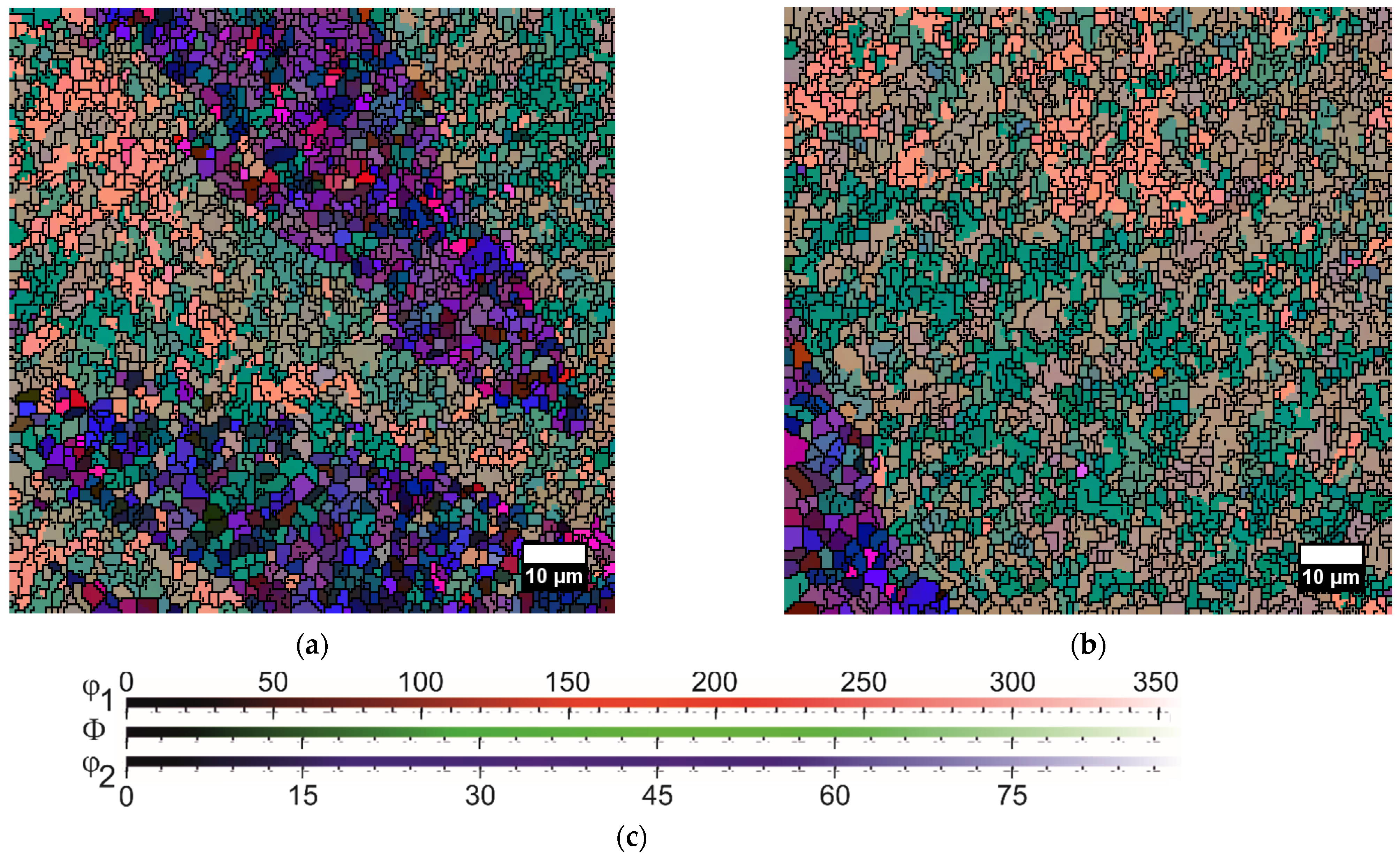
To study possible structural changes in the NSDL of Al wires, the measurements were carried out on longitudinal sections and cross-sections at two points of each sample, namely in the center of the section and at a distance of ~100 μm from the edge. To investigate the effect of the wires’ operating time on the wires’ grain structure, the sample N5 (new) and the sample N8 (after ten years of operation) were selected. The maps of distribution of Euler orientation angles φ1, Φ, and φ2 (correspondingly, angles of intrinsic rotation, nutation, and precession, see definition in [38]) with superimposed grain boundaries are shown in Figure 3 and Figure 4 for the transverse (near the edge of the samples) and longitudinal (near the edge for both samples as well as in the center for the N8 wire after ten years of operation) sections, respectively. Maps taken in the center of the facet for the cross-section of the two wires and the longitudinal section of the new sample N5 are presented in [9] in Figure 8a,b,f, respectively. The color of a pixel on the maps corresponds to a combination of Euler angles describing the orientation of the crystal lattice at a given point. On longitudinal-section maps, the axis of the wire is directed vertically.
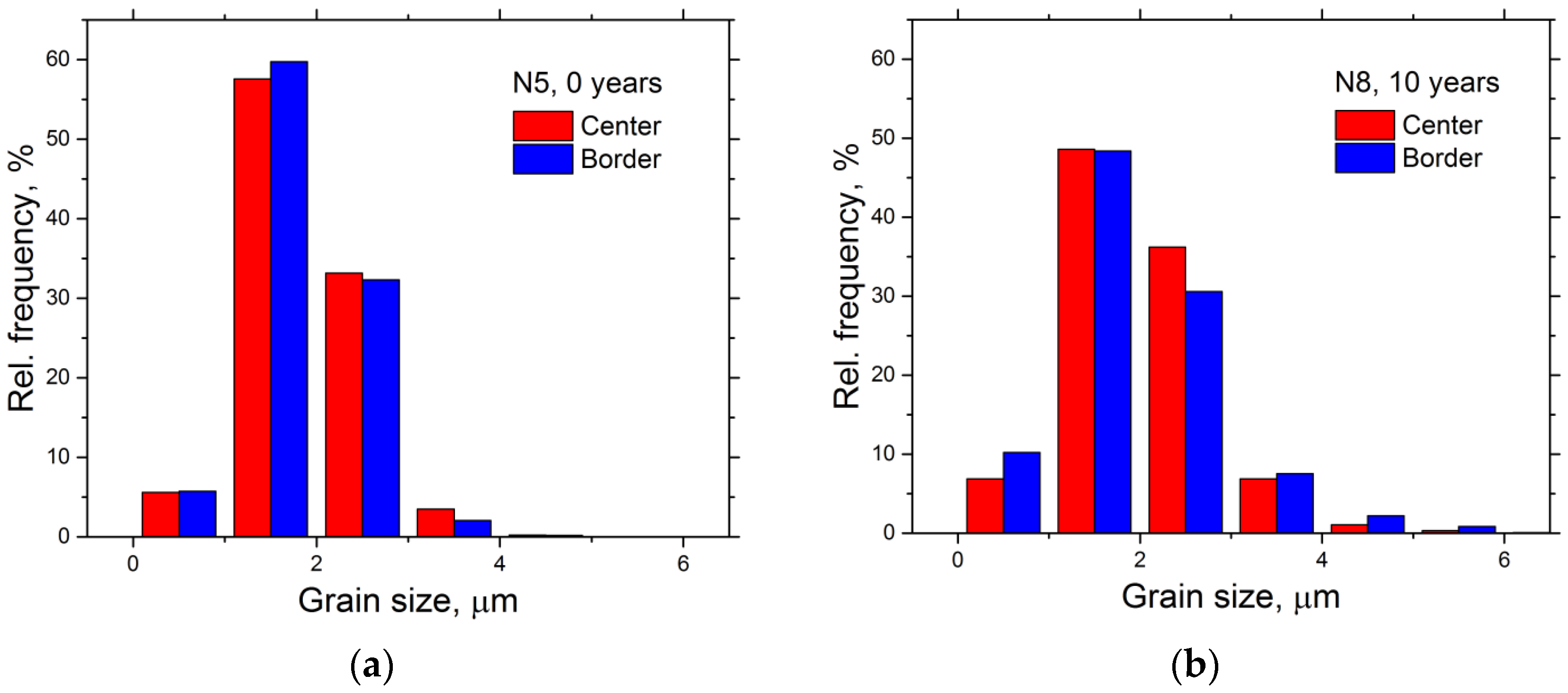
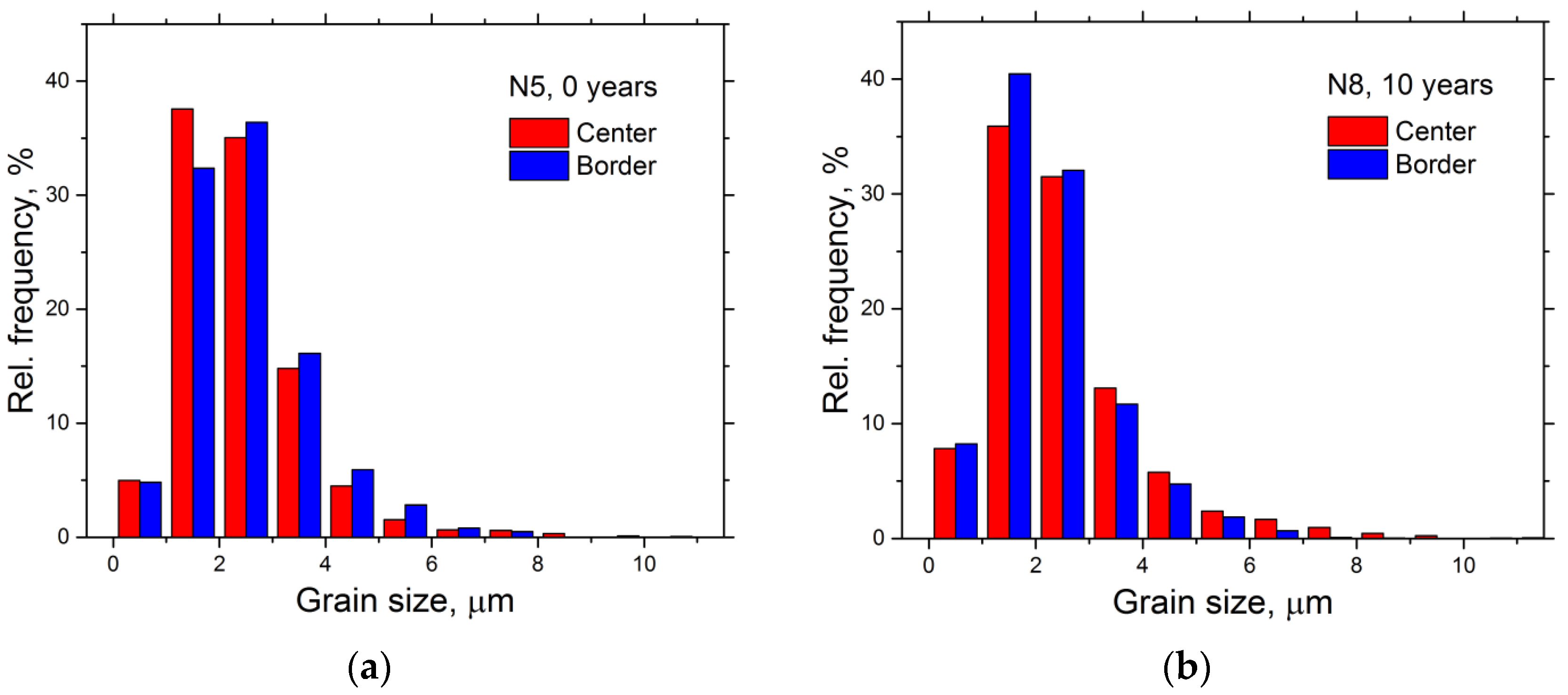
As a result of the analysis of the maps, grain-size distributions were built (Figure 5 and Figure 6). It can be seen that for both samples, new (N5) and after ten years of operation (N8), the size of most grains is 1-4 μm in the center (i.e., inside the wire) and near the edge in the longitudinal section and 1-3 μm in the center and near the edge in the cross section (Figure 5 and Figure 6). As noted earlier in [9], for internal cross-sectional areas (i.e., in the center of the cross-section) of wires with a service life of up to 62 years, operation in an ambient air atmosphere conditions leads to a decrease in the number of grains from 1 to 3 μm in size and the formation of a small number (<1% relative frequency) of larger grains from 3.5 to 5 μm in size. For the edges of the cross-section, this effect looks more pronounced (about 3%), and the maximum grain size increases to ~6 μm (Figure 5b). A similar effect after the operation of the wires is observed for the longitudinal section. Along with a decrease in the number of grains with dimensions of 1 to 4 μm in the center and on the edge, a larger number of grains (~2–3%) of even larger size ~6 to 10 microns is formed, and there are more such grains in the center of the longitudinal section (cf. Figure 6a,b).
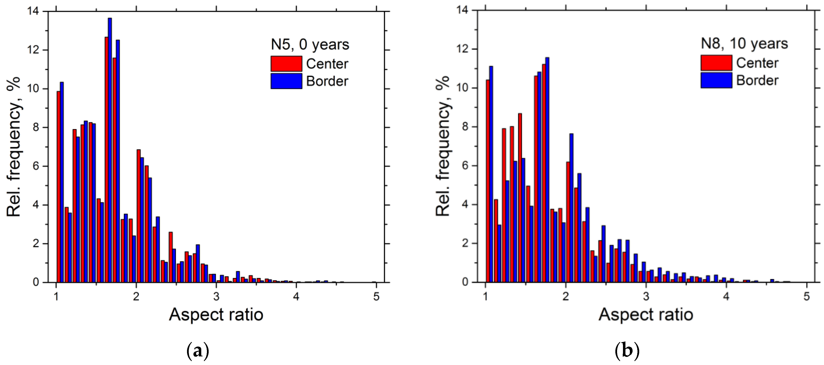
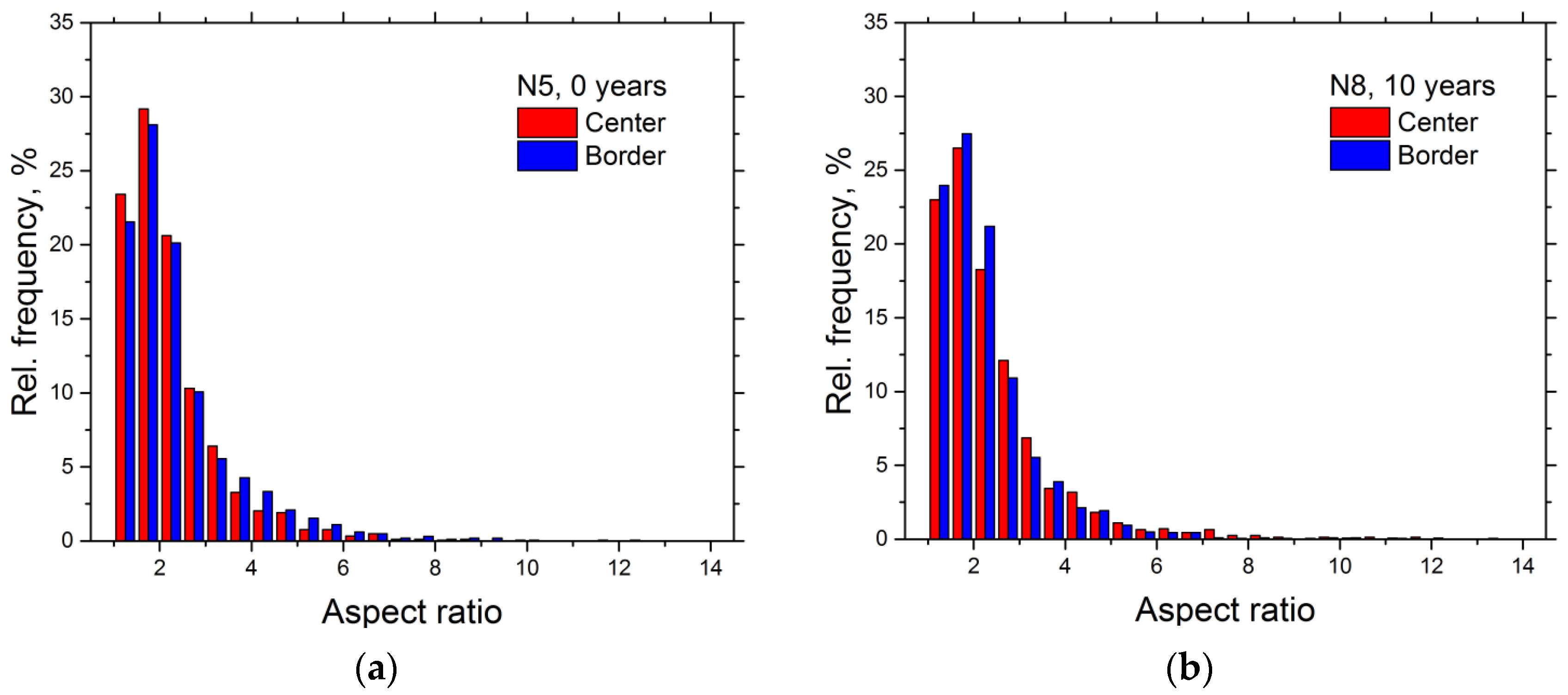
Figure 7 and Figure 8 present the histograms of the distribution of the aspect ratios of grains (the ratio of the maximum grain size to the minimum one). It can be seen that the aspect ratio of most grains is one to eight for longitudinal and one to four for cross sections, both for the center and for the edge of the sample, for new and after ten years of operation. Thus, the grains have an elongated shape along the axis of the wire (corresponding to higher values of the aspect ratios) relative to the cross-section, which is retained during the operation of the wire.
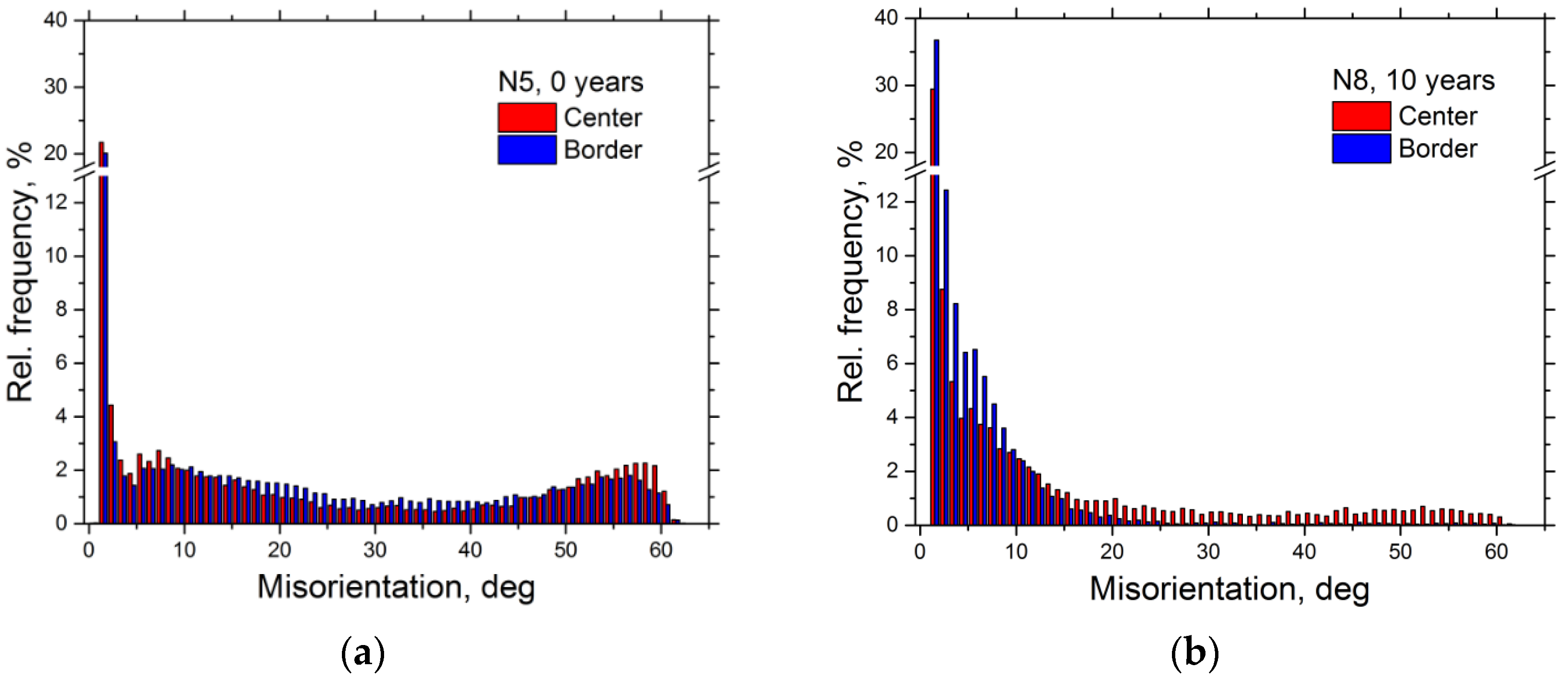
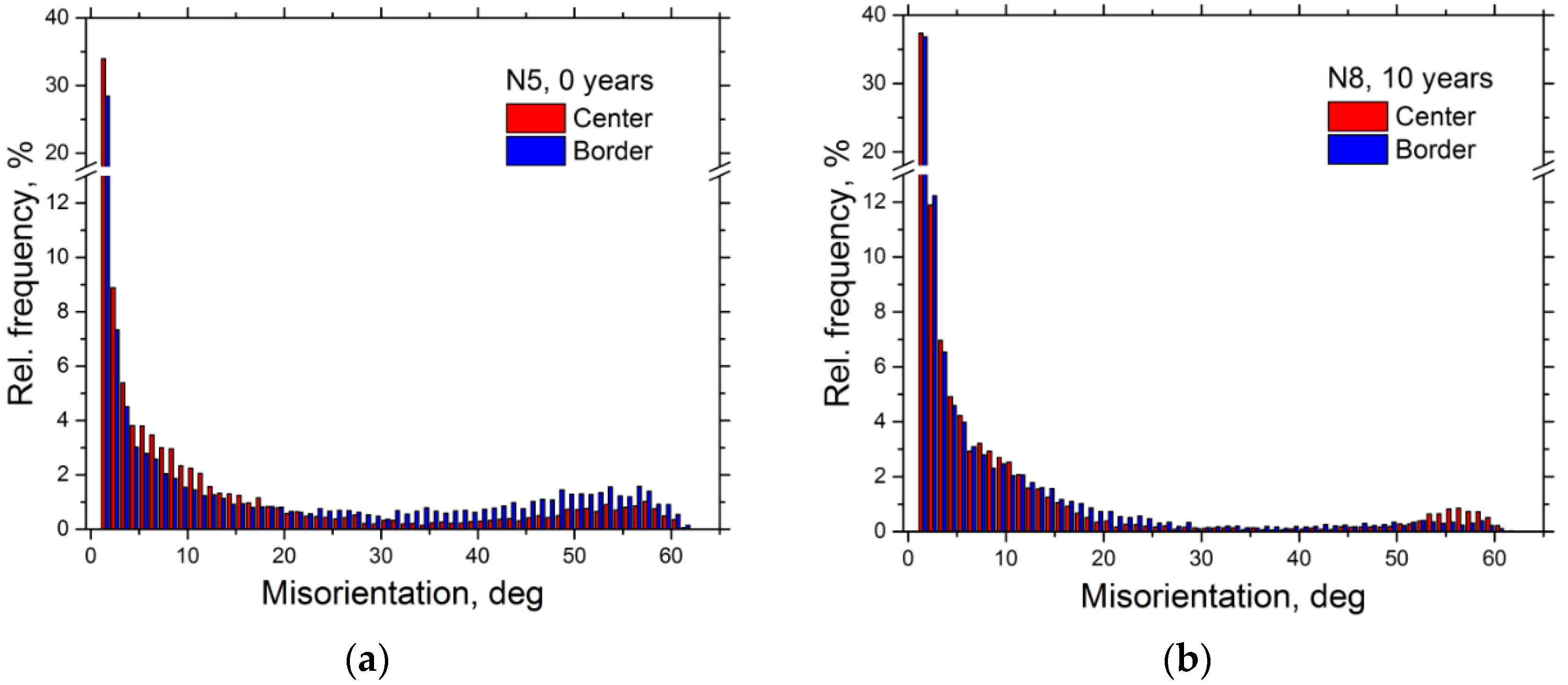
Histograms of the distribution of the angles of misorientation of grain boundaries were also constructed (Figure 9 and Figure 10). With an increase in the operating time of wires, a decrease in high-angle boundaries (misorientation more than 15°) in the cross section and an increase in low-angle boundaries (misorientation less than 15°) are observed. A similar dependence is observed in the case of a longitudinal section.
The analysis of grain distributions by misorientations showed the following. In the new sample both for the cross and longitudinal sections, no noticeable differences are observed between the NSDL and the central part. In the entire volume of the sample, a significant number of both low-angle boundaries and boundaries with large misorientations (peak at misorientation angles of 50–60°) were found both in the longitudinal and transverse directions.
In the cross sections of the wires after ten years of operation (N8), a significant decrease in high-angle boundaries in the central part was revealed in comparison with the new sample N5. In the NSDL, high-angle boundaries are practically absent (Figure 9b). A similar picture is observed for the longitudinal section (Figure 10b).
Thus, the maps constructed by EBSD have shown the similarity of the grain structure in terms of grain size and their aspect ratio (i.e., grain shape) in the center and at the edge of the cross- and longitudinal sections of the wires both before and after operation. However, the defect near-surface region (i.e., NSDL) has a noticeable effect on grain misorientation. High-angle boundaries between grains were practically disappearing in the NSDL.

3.4. XRD Results

XRD patterns measured from all wire samples are given in [9]. These XRD patterns show the full set of reflections of polycrystalline Al (space group F m 3 ¯ m , PDF-2 entry 01-073-9843). As an example, Figure 11 presents the X-ray patterns of wires N5-2 (new, zero years of service) and N6-2 (62 years of service), the low intensities being upscaled to show the appearance of crystalline alumina reflections after years of service. Some of the reflections attributed to polycrystalline aluminum oxides δ- and/or δ*-Al2O3 [39,40] (PDF-2 entries 00-056-1186 and 00-046-125, respectively) begin to form already at least after ten years of operation, reaching a maximum in intensity of reflections (~0.7% of the maximum-intensity Al reflection) after 62 years of operation [9]. The change in the intensity of X-ray reflections observed in Figure 11a,b with a change in the operating time from 0 to 62 years is discussed in detail in [9] and is associated with the development of a preferential orientation along the crystallographic direction [011] in the crystal lattice of Al wires due to the growth of crystallites and grains after the operation of the wires.
Figure 12 shows the X-ray penetration depths Tpen into the Al wire versus the 2θ X-ray diffraction angles (for two samples with different service life taken as an example). Each point in this Figure 12 corresponds to the penetration depth T p e n h k l calculated with Formula (2) and corresponding to the Al reflection with Miller indices hkl and Bragg angle 2θB (i.e., 2θ = 2θB).
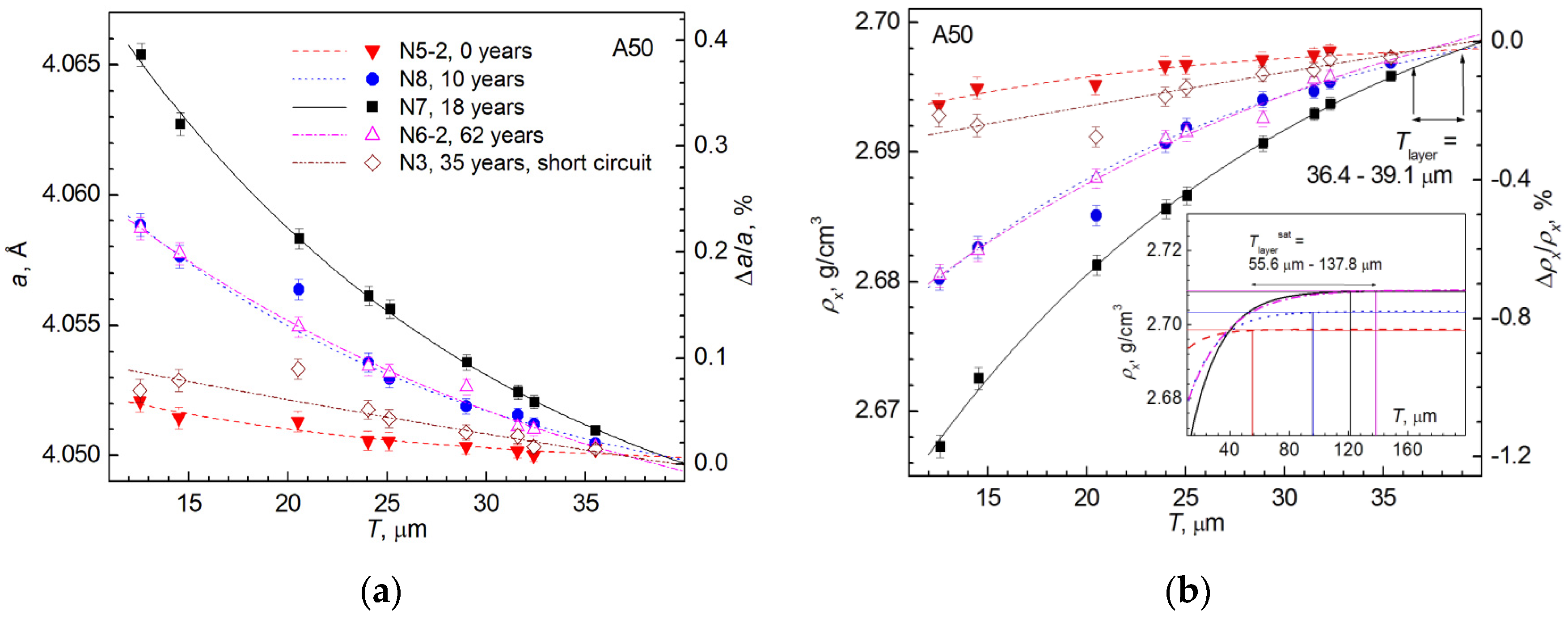
Using this relationship between Tpen and 2θ presented in Figure 12, the distributions of the Al cubic unit-cell parameter a (calculated from Bragg’s law after making the necessary angular corrections, see Section 2.3) were obtained over the depth T from the surface of the Al wire (Figure 13a). Depicted by a symbol, each experimental point in this graph corresponds to the depth T p e n h k l of penetration of X-ray radiation into the Al wire material, related to the reflection with Miller indices hkl. After recalculation with Formula (3), the profiles of the mass X-ray density ρx(T) of the Al material in the NSDL up to T ≈ 36 μm deep were obtained from the a(T) dependences (Figure 13b).
One can see from Figure 13a,b that the experimental points obtained for wires of different service life show systematic changes with increasing X-ray penetration depth. Near the surface (~12 μm deep), the Al cubic unit-cell parameter a is maximum and decreases when retreating from the surface inward to ~36 μm. Accordingly, the density ρx is minimum at the surface and increases with distance from the surface. All experimental points with the exception of wire N3 (after a short circuit) are rather well described with the approximation exponential-decay curves ρx(T) (with a negative multiplier before the exponent function, which, with an increase in the depth T from the surface, reach the “saturation plateau”, practically parallel (within ~3 × 10⁻⁵ g/cm3) to the T axis. On the right sides of Figure 13a,b, additional axes are shown, respectively, for the lattice defect Δa/a and the density defect Δρx/ρx, estimated with Formulas (5) and (4), where the values of the unit cell parameter and mass density in the volume of the new wire, a0 = 4.04967 Å and ρx0 = 2.69847 g/cm3, are taken as ones corresponding to the plateau of the approximation curve ρx(T) of the new wire N5-2. Since changes in the parameter a of the cubic unit cell of the Al wire material and its mass density ρx, which are estimated from it with the use of structural data and Formula (3), are related as ρx~1/a3, then we will track changes in ρx, since this physical parameter is significant to interpret the condition of wires after operation in overhead power lines and is measured and used in densitometric and acoustic studies.
Thus, all samples including the new sample N5-2 show a systematic, identical in nature (described by the exponential-decay function) decrease in the cubic unit-cell parameter and an increase in mass density calculated from the structural data, i.e., experimental XRD pattern. In this respect, the only exception is wire N3 after a short circuit, in which the exponential-decay function degenerates into an almost straight line in the region up to 36 μm depth.
However, depending on the operating time, the density defect Δρx/ρx (the change in ρx relative to the ρx0 value on the plateau of the approximation curve of the new sample) changes significantly with depth from the surface. Whereas Δρx/ρx ≈ 0% at a depth of T ≈ 36 μm for all samples, near the surface (T ≈ 12 μm) the density defect is maximum in absolute value but noticeably different depending on the service life of the wires (Figure 13b). Nonzero Δρx/ρx ≈ −0.17% near the surface at a depth of T ≈ 12 μm is already present in the new sample, increasing in absolute value to Δρx/ρx ≈ −1.17% for sample N7 after 18 years of operation. The experimental points Δρx/ρx for a wire with a maximum service life of 62 years practically coincide with Δρx/ρx for a wire after ten years of operation, and after a short circuit they are close to the values in a new wire. Similar results for these samples were previously obtained when calculating the Δρx/ρx value averaged over a layer with a thickness of ≈ 36 μm [9]. An increase in the amplitude Δρx/ρx(T) in the NSDL of wires from T ≈ 12 to 36 μm depth when service life increases up to 18 years is explained by an increase in the concentration of void defects (microcracks, microvoids, pores) at the corresponding depths from surface. This concentration is naturally higher near the surface. The Δρx/ρx(T) relaxation in the sample after 62 years of service is probably associated with the healing of voids due to the growth of δ- and/or δ*-Al2O3 crystallites, the formation of which, according to XRD studies, increases with increasing service life. In the N3 wire after a break due to a short circuit and burning, voids are healed under the high-temperature influence. At the same time, they remain in the bulk and their concentration even increases, as was shown by densitometry measurements in [9].
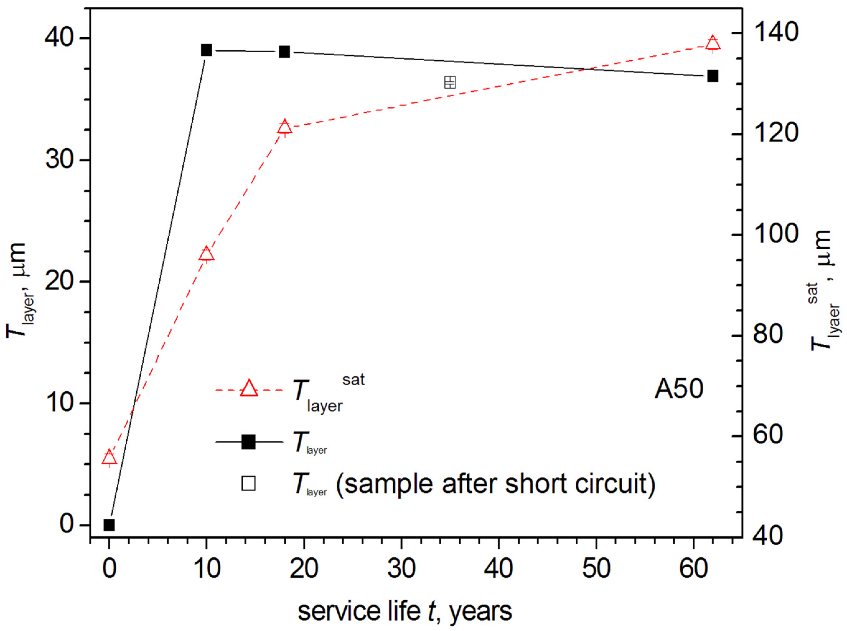
If we neglect a NSDL in the new sample (taking into account the small absolute value of density changes in this layer, Δρx/ρx ≈ −0.17% near the surface at a depth of T ≈ 12 μm), then the thickness of the NSDL in other samples can be estimated from the intersections of the approximation curves ρx(T) with the approximation curve of the new sample. In this case, the thickness of the NSDL Tlayer = 36.9(1) − 39.1(1) μm with an average value of Tlayer = 38.3(1.2) μm for whole service life of wires that have served without damage, i.e., it practically does not change (Figure 14). For a sample after a short circuit, the defective-layer size estimated in a similar way shows a comparable, albeit somewhat lower, value Tlayer = 36.4(1) μm, possibly because of the partial destruction of this layer due to high temperatures during short circuit and burning. Similar values of a defective corrosion layer of 20–40 μm were obtained in Al panels that stood for 13–16 years in an agricultural or urban atmosphere in Spain [10]. Close values of the thickness of the defect layer Tlayer for wires of different service life including a much longer one seem to require clarification.
However, it should be taken into account that the new wire also demonstrates the ρx(T) distribution, although not as large in amplitude as the wires after operation (Figure 13b). The new wire also has its own defect layer, which appears, probably, due to the conditions of preparation, rolling, processing, etc., although difference in the mass density of Al material near and far from the surface being not so large. To determine the defect-layer thickness in the new wire and in the other ones, the “tangents” to the plateau of the approximation curves ρx(T) were drawn in the form of exponential-decay functions (see the inset in Figure 13b). The “tangential” lines were drawn at the points when ρx reaches the plateau value ρxsat = 99.99% of the density ρx200μm estimated from the approximated distribution curve at a depth of 200 μm. The ρx500μm estimation at a depth of 500 μm differs from the ρx200μm one by only 0.001%, which implies that ρxsat is a fairly good approximation of the density plateau.
From the intersection of “tangent” lines drawn in a similar way with the approximation curves ρx(T) in the form of exponential-decay functions, the values of the defect layer approximation thickness Tlayersat were determined, being 56(1) μm in new samples and 96(1) to 138(1) μm in samples after operation with an increase in service life from 10 to 62 years (Figure 14). This is comparable to the thickness of the corrosion NSDLs of ~100 μm in ACSR wires of overhead power lines operated in the industrial atmosphere of the Czech Republic for 40 years [8]. The growth rate of the thickness Tlayersat of the defect layer in the investigated Al wires from AAAC overhead power lines of the A50 type, which was estimated at the interval from 0 to 18 years, where the points of the time dependence practically fall on a straight line, is vcor = 3.7(3) μm/years. This rate value is close to the corrosion rate vcor ~5 μm/years for Al wires from ACSR overhead power lines in the industrial atmosphere of the Czech Republic [8]. With a further increase in the service life from 18 to 62 years (only two points), the growth rate of the thickness of the defect layer in the AAAC wires studied decreases to vcor ~0.4 μm/years; although this time interval requires further research.
For sample N3 after a short circuit, estimates carried out in a similar way give a much larger value of the approximate thickness of the defective layer Tlayersat~850 µm, which can be attributed to the influence of electromagnetic exposure and high temperatures during a short circuit and ignition. However, this sample requires a separate study by various methods and was excluded from the analysis.
The values of the defect layer thicknesses Tlayersat obtained from the intersections of the approximation curves and tangents to the plateau, drawn at the points when ρxsat reaches the ρxsat value of 99.99% of ρx200μm, correspond to ρ x 12 μ m ρ x s a t ρ x 12 μ m ρ x 200 μ m ~99% of the ρx drop when the depth decreases from T = Tlayersat to the surface (T ≤ 12 μm) as estimated from the approximation curves ρx(T) at depths of 12 μm up to 200 μm. The thicknesses Tlayer obtained when neglecting the defect layer of the new wire from the intersection of the approximation dependences ρx(T) with ρx(T) of the new sample correspond to ~99.6% of ρx200μm. At the depths equal to Tlayer, ρ x 12 μ m ρ x l a y e r ρ x 12 μ m ρ x 200 μ m ~70% (i.e., the most part) of the decrease in the density ρx occurs when the depth decreases from T = Tlayer to the surface (T ≤ 12 μm), here ρxlayer being the mass density ρx at the depth of Tlayer. It is worth to note that for the new sample (N5-2), 70% change of the total decrease in the density of ρx in comparison to the value ρx200μm in the bulk occurs at a depth of Tlayer = 30.1(1) µm from the surface, which is comparable to the average value of Tlayer = 38.3(1.2) µm for wires after operation.
In order to obtain evidence of the validity of this approach to determining the total thickness Tlayersat of the NSDL, a wire sample N7 (18 years of operation) with the most significant density defect Δρx/ρx of the NS in the NSDL was examined by means of XRD after etching the sample in NaOH. The thickness of the removed layer of 53 μm is calculated according to Formula (10) using the measured mass of the sample before and after etching. Thus, the expected thickness Tlayersat of the NSDL should be equal to ~68 μm, while the density defect in absolute magnitude should decrease to a value of about −0.2%. The values obtained after analyzing the XRD pattern of wire N7 after etching (Supplementary Materials, Figure S5), Tlayersat = 86 μm and density defect Δρx/ρx = −0.15%, are in satisfactory agreement with the expected values, taking into account possible inaccuracies of densitometry and XRD experiments and calculations.
The mass density ρxsat and the parameter of the cubic-unit cell asat at a depth of Tlayersat (Figure 15) correspond to the values of these parameters of the Al-wire material in the bulk, far from the surface. For the new wire, these values differ slightly (by 0.07% more for ρxsat and by 0.03% less for asat) from the corresponding values a = 4.050694 Å from the powder database (PDF-2 entry 01 -071-4008) and calculated ρx = 2.69642 g/cm3 for the 312.3 K temperature, which is comparable to the XRD temperature of 314(1) K at measurements in this work. Apparently [9], this difference is associated with the presence of Si and Fe impurities in Al wires, as shown by the determination of their elemental composition by the EDX method. With an increase in the service life up to 18 years, ρxsat is already 0.46% higher, then remaining practically the same for up to 62 years of service. Agreeably, the cubic unit-cell parameter decreases by 0.15% after 18 years and 0.16% after 62 years of service. Simultaneously, EDX shows an increase in oxygen content after use, and XRD measurements detect the formation of Al oxides (δ- and/or δ *-Al2O3), for which an increase in density is associated with [9]. Probably, the growth of Al oxide crystallites leads to the compression of the cells of the Al material, the calculated density ρxsat increasing as a result.
As already noted in Section 2.3, in the presence of only one reflection, it is possible to determine either only the value of the crystallite size D at a fixed value of microstrain εs in it or only the value of microstrain εs at a fixed value of D.
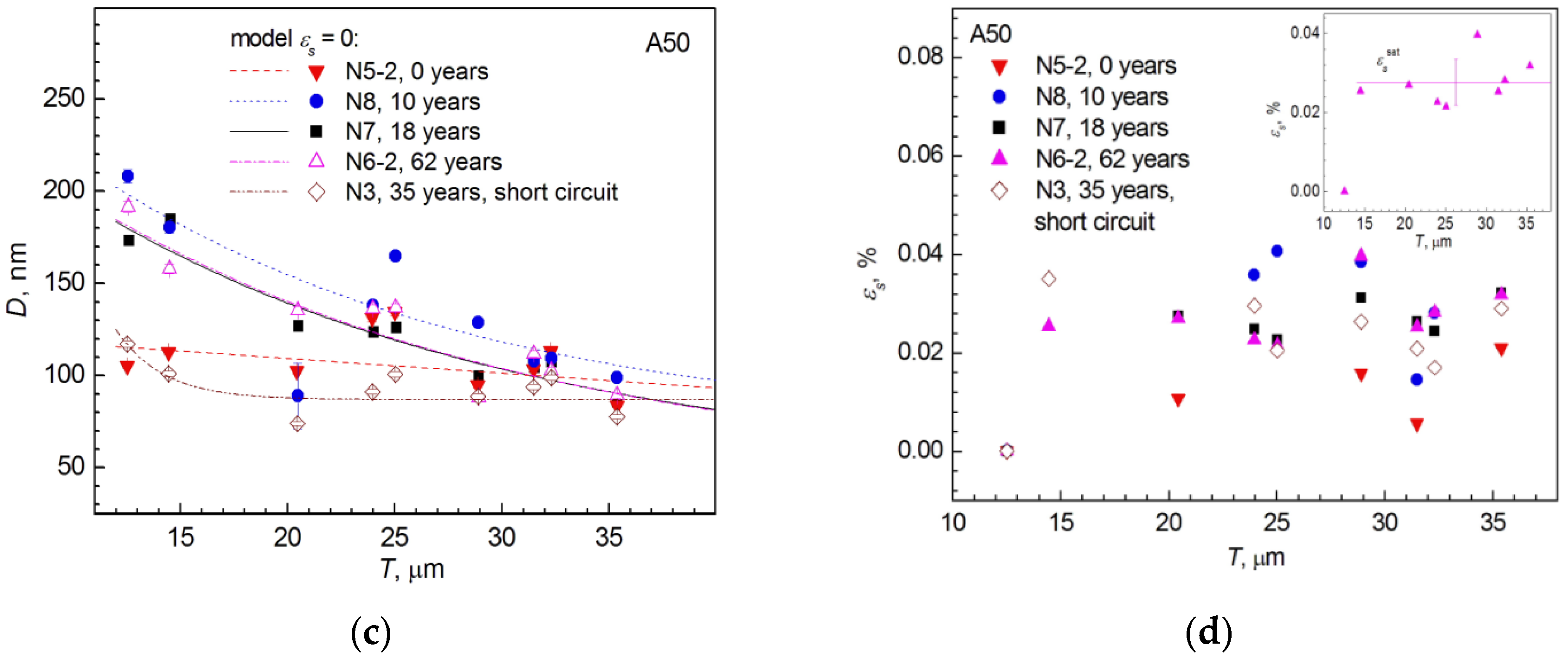
Figure 13c shows the size distribution Dεs=0 of crystallites in the NSDL up to ~36 μm deep, calculated from the observed FWHMobs reflections (after correction for instrumental broadening with Formula (7)) in the approximation of zero microstrain (εs = 0) according to the Scherrer law, Formula (6). As can be seen, the distributions of crystallite sizes Dεs=0(T) are qualitatively very similar to the distributions of the Al-material cubic unit-cell of parameter a(T) in the NSDL (cf. Figure 13a,c). A much larger spread of the experimental values Dεs=0 relative to the approximation curves indicates an insufficiently high accuracy of estimating this value and does not allow quantitative estimates of the thickness of the NSDL.
At small depths (~12 μm), the sizes of crystallites Dεs=0 are quite large (from ~110 nm for a new sample (N5-2, 0 years in service) and a wire after a short circuit (N3) to ~200 nm for samples after operation without damage for 10–62 years) and decrease to ~90 nm at a depth of ~36 μm for all wires. As in the case of the a(T) distribution, the difference between the values Dεs=0 for the new wire and wire after a short circuit near (T~12 μm) and far (T~36 μm) from the surface is small, merely about 20%. For wires after operation without damage for 10–62 years, the difference reaches ~200%, the only distinction being that the maximum difference appears not in the 18-year-old wire (N7), but in the N8 wire after ten years of operation. In its turn, relaxation of the wire after 62 years of operation (in terms of the sizes of crystallites in the NSDL, Dεs=0, at different depths up to T~36 μm) occurs not to the state after ten years of operation, as in the case of the lattice parameter, but to the state after 18 years of operation. A similar shift to the maximum size of crystallites, D, averaged over the entire surface layer up to T~36 μm deep after ten years of operation was previously found in [9] for the wires under study.
It should be noted that, by means of the WHP and SSP methods, the value εs~0 was obtained for all reflections in the new wire, while the presence of microstrain was detected in the samples after operation. The microstrain averaged over the entire surface layer 36 μm thick had an average value εs~0.30% in wires that have worked normally (without short circuit or cable breakage) and εs~0.20% in the wire after a short circuit. When these fixed values are specified, the estimates of D increase in comparison with Dεs = 0 by a factor of ~1.4 in a ten-year wire, by a factor of ~2.2 in wires after 18 and 62 years of operation, and by a factor of ~1.25 in a wire after a short circuit.
Figure 13d shows the results of calculation of the distribution of the absolute values of microstrains over the depth T from the surface. These values were calculated for each reflection hkl using Formulas (6), (8) and (9) under the assumption of the crystallite size D fixed at the Dεs=0 value found for the Al reflection hkl = 111, corresponding to the minimum penetration depth of X-rays of ~12 μm (if the system of equations had no solution for a reflection, this point was not shown in Figure 13d).
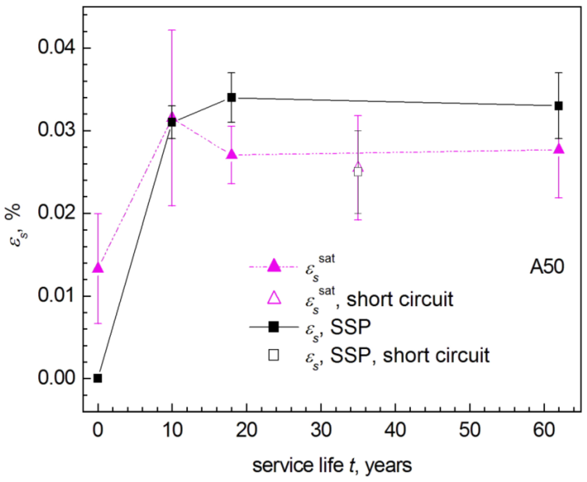
As one can see from Figure 13c, the crystallite size at the surface (T~12 μm) is maximum for most wires after various service lives. In this case, there are no microstrains (εs = 0) near the surface (T~12 μm) of all wires. However, already at a depth of T~15 μm, microstrains sharply increase and show a scatter about the average value of εssat with an increase in the depth from the surface to T~36 μm (see the inset in Figure 13d as an example). Nonzero values of microstrain εssat~0.01% at depths T > 15 μm are already present in the new wire, increasing to εssat~0.031–0.027% after operation for 10–62 years, only weakly falling to εssat~0.025% after a short circuit. The εssat change depending on the service life (Figure 16) is similar to the change in the mean microstrain εs, averaged over all XRD reflections arising from the maximum experimentally achieved penetration depth of ~36 μm, presented in [9]. As the estimates show, the similarity of the dependences εssat(t) and εs(t) will be even greater if one takes into account the possibility of a systematic decrease in the size D of crystallites with a retreat from the surface inward, similar to the dependence Dεs=0 on the depth T, which was estimated for the case of zero microstrain (Figure 13c) albeit with a smaller scatter of the D values at different depths.

3.5. Results of Densitometric Measurements

Earlier [9], XRD methods had shown that, with an increase in the service life of wires of overhead power lines, the formation of δ- and/or δ*-Al2O3 was observed in the near-surface layer. The oxide volume fraction increases with increasing service life and reaches a maximum for samples after 62 years of service. This factor could explain the fact that the integral density of the samples decreased with a service life from 0 to 35 years, but as it was found, slightly increased by 62 years (since the value ρ ≈ 3.7 g/cm3 for aluminum oxides is significantly higher than the density of the Al metal, ρAl ≈ 2.7 g/cm3). From this point of view, just the increase in the volume fraction of oxides compensated for the decrease in the mass density caused by the formation and development of microvoids in the surface layer of wires under prolonged loading (tensile loads, vibrations, etc.).
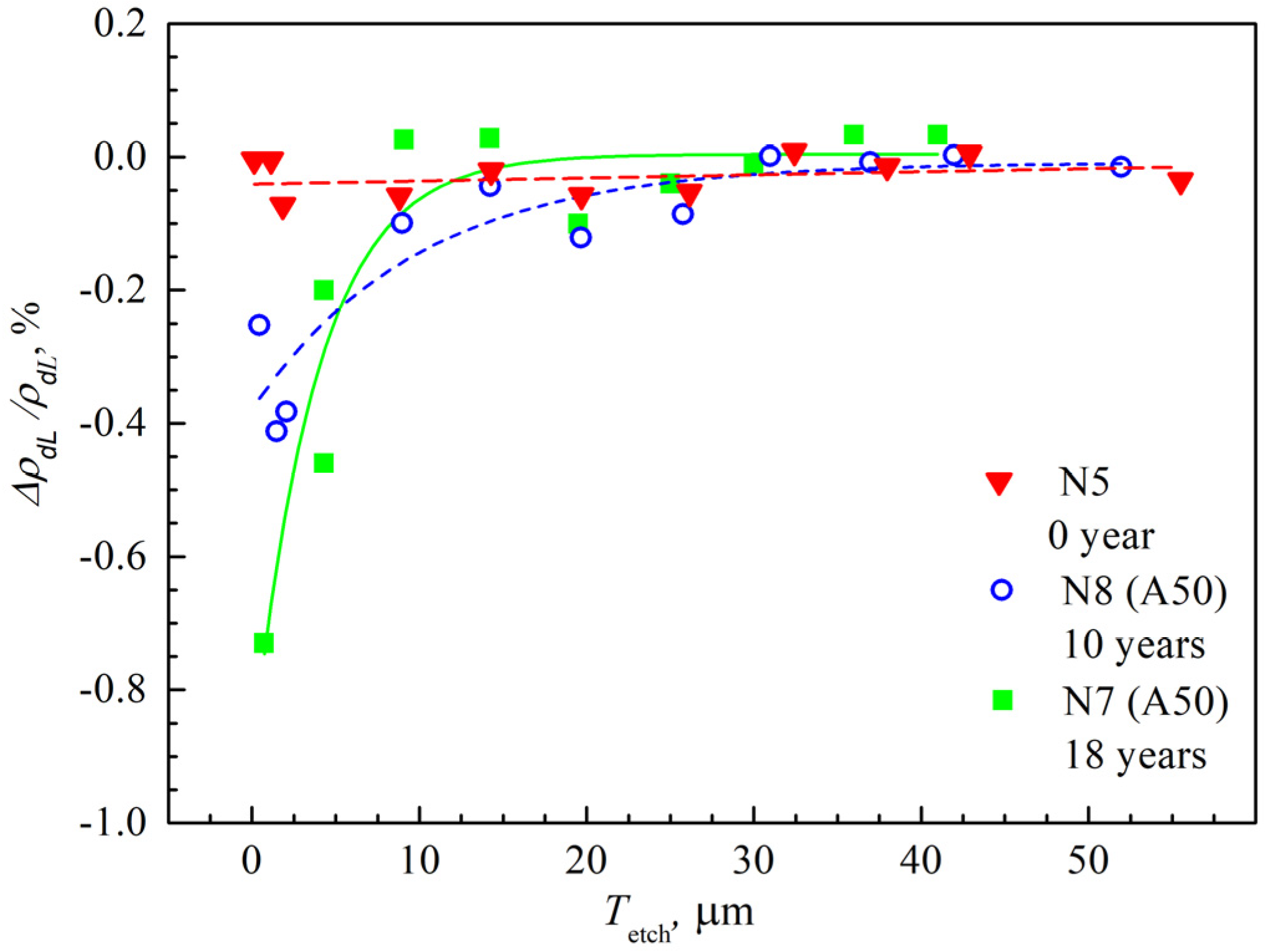
To correctly estimate mass density distribution over the cross section of the samples by the densitometric method, samples N5 (0 years), N8 (10 years), and N7 (18 years) were selected. Figure 17 presents the density-defect distribution, ΔρdL/ρdL (in %) over the section for the wire samples under study. Measurement of the density of the new sample (N5, without operation) did not reveal any changes in its density values with the successive removal of layers, which indicates the relative homogeneity of the material. As follows from the graph analysis, the absolute value of the density defect ΔρdL/ρdL for samples after operation for 10 and 18 years decreases with an increase in the thickness Tetch of the removed layer. The highest in absolute value density of defects of a void nature (decrease in mass density) is concentrated in the surface layer~12 μm. Nevertheless, according to the data obtained, a change in ΔρdL/ρdL is observed until the removal of ~30 μm of the surface layer. When comparing the data for samples N8 and N7, it can be noted that the defectiveness of the layer almost doubles during service life of 10 to 18 years.

3.6. Changes of Elastic and Microplastic Properties of Wires after Etching

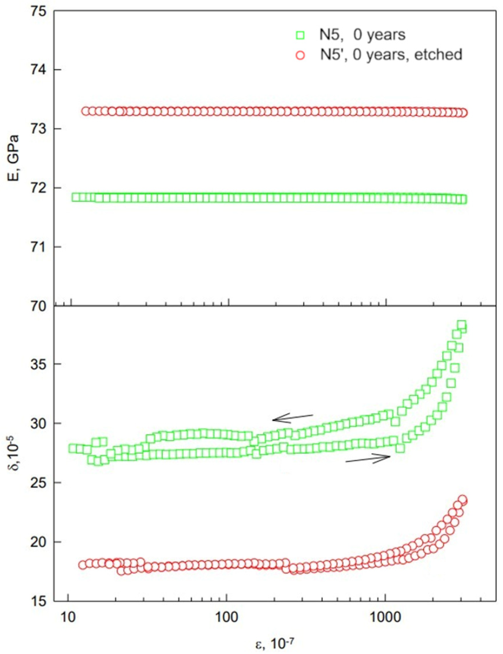
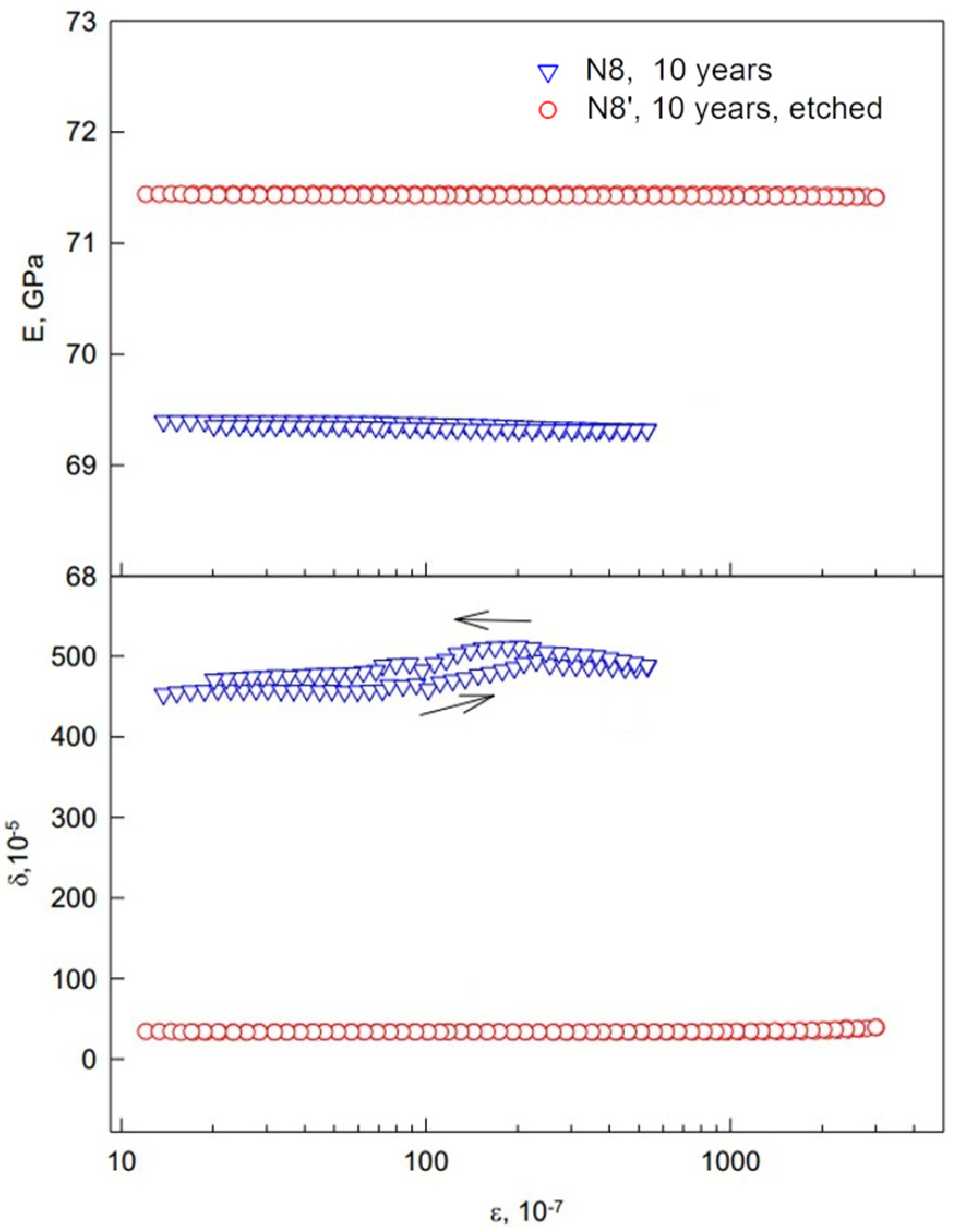
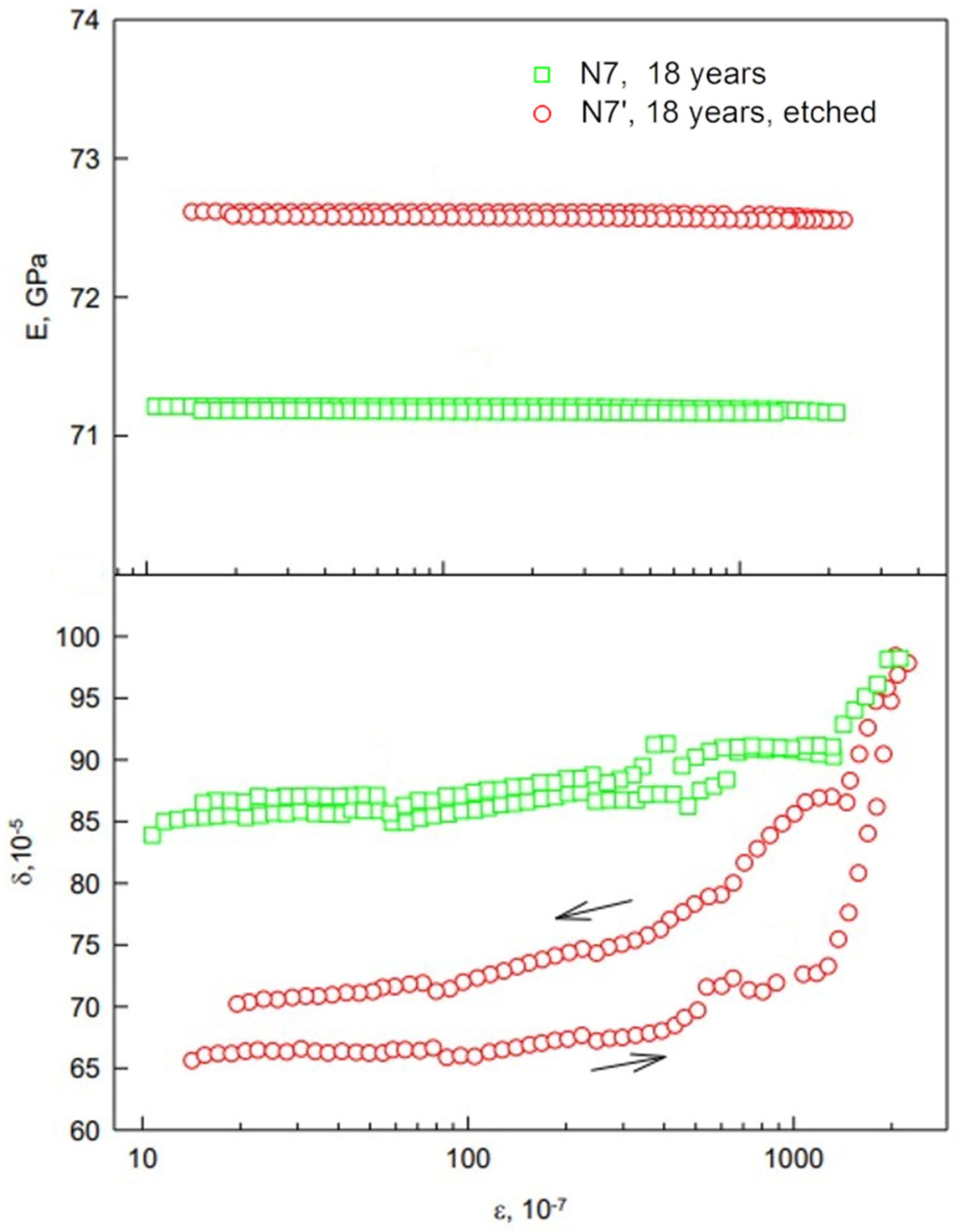
Let us proceed to consider the results of changes in elastic and microplastic properties after removal of the damaged surface layer. Figure 18, Figure 19 and Figure 20 show the amplitude dependences of Young’s modulus E and decrement δ for the A50-type wire samples before and after removing the surface layer with a thickness Tetch of about 35 μm. The dependences E(ε) and δ(ε) were measured sequentially with an increase and decrease in the amplitude of vibrational strain ε. The generality, which attracts attention first of all, is an increase in the elastic modulus E and a decrease in the decrement δ with the removal of the surface layer for all samples. For Young’s modulus E, this change is about 1.5 GPa on average. In detail, for N5 (new sample), the elastic modulus increased from E = 71.8 GPa to E = 73.2 GPa, for N8 (service life of 10 years) from E = 69.4 GPa to E = 71.4 GPa, for N7 (18 years) from E = 71.2 GPa to E = 72.4 GPa. For the decrement δ, the most significant change is observed for sample N8 (service life of ten years), namely there is more than a ten-fold decrease. However, it should be noted that the decrement of sample N8 had the highest value among all the studied service lives. Therefore, its significant drop upon removing the surface layer indicates that most possible effects are mainly due to this layer. The decrement decrease ranged from δ = 27 × 10−5 to 17 × 10−5 for sample N5 (new) and from δ = 85 × 10−5 to 65 × 10−5 for sample N7 (service life of 18 years).
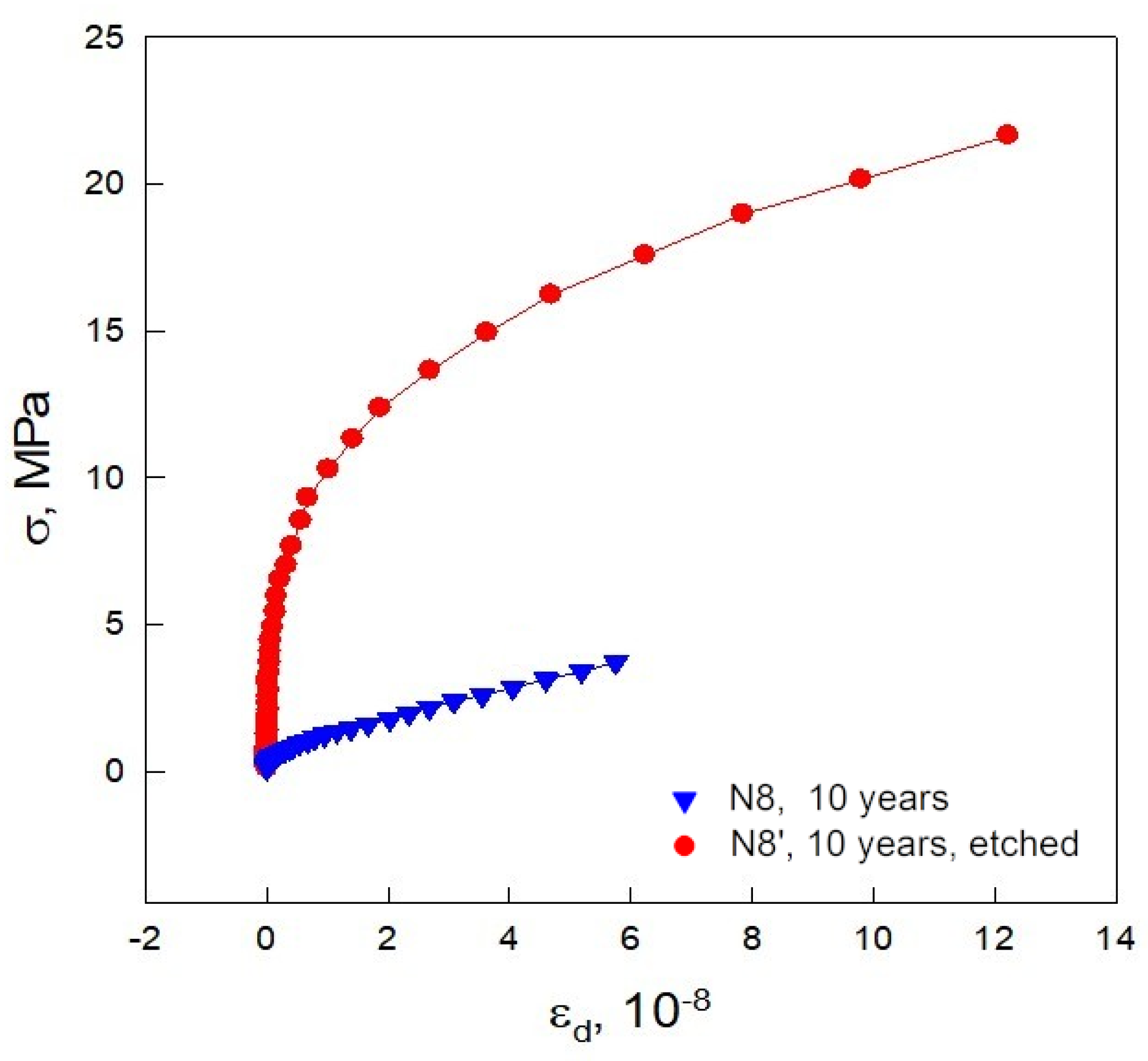
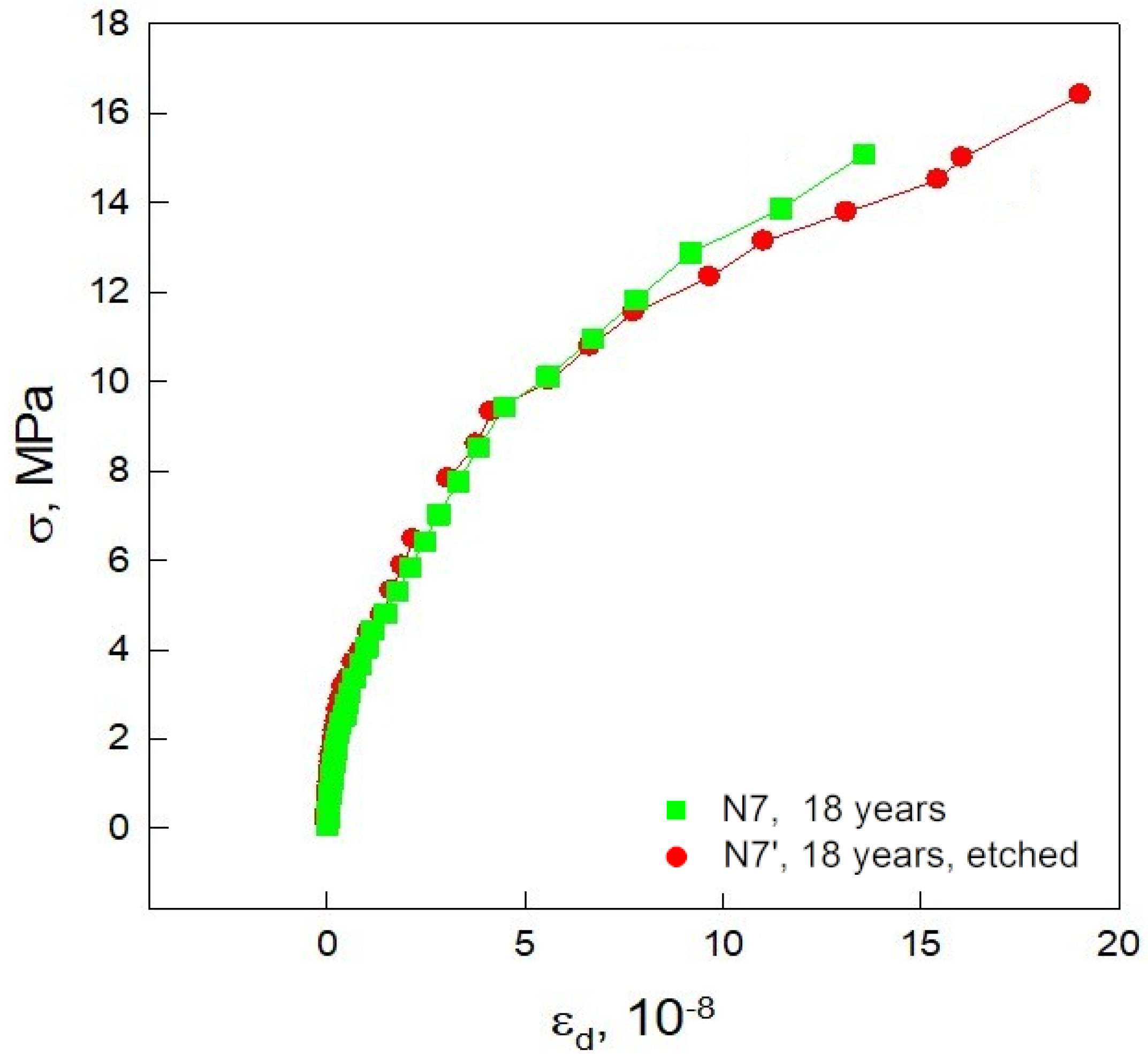
Figure 21, Figure 22 and Figure 23 show diagrams of microplastic strain of wire samples before and after etching. The diagrams are obtained from the dependences E(ε) shown in Figure 18, Figure 19 and Figure 20 and taken at the first increase in amplitude ε. Here, as in the case with the modulus, the removal of the surface layer led to an increase in the stress σs of the microplastic flow. This effect was most pronounced for sample N8 (ten years of service), where σs increased by about nine times (comparison is given for inelastic strain εd = 1 × 10⁻⁷). For a more convenient comparative analysis of all samples, Table 2 presents the numerical values of the density ρd based on the results of densitometric measurements, the elastic modulus E, the amplitude-independent decrement δi, and the micro-flow stress σs at inelastic strain εd = 5.0 × 10⁻⁸.
Let us analyze the obtained data on elastic and microplastic properties. It is known that the material mass density has a direct effect on the value of its modulus of elasticity [41,42]. Removal of the damaged surface layer leads to some increase in the density of the samples under study. However, this change in density is so small (fractions of a percent) that it is difficult to have a significant effect on the change in modulus, an increase in which on average was 2–3%, only due to the influence of defects of a void nature. Another factor that could lead to an increase in the modulus in this case is a decrease in the dislocation density. Indeed, in the process of manufacturing the wires (both when obtaining individual elements of cores (wires) and when creating a core), the aluminum alloy undergoes various kinds of plastic deformations, which can lead to an increase in the density of dislocations. According to the theory of internal friction, which describes the interaction of dislocations with point defects, Young’s modulus should increase and the decrement should decrease as a result of a decrease in the density of dislocations [33,43]. Therefore, the observed changes in the properties of elastic and microplastic properties (Table 2) seem to be natural, removal of the damaged layer leads to an increase in E and a decrease in δi. The same circumstance can explain the observed decrement hysteresis for samples N5 (new) and N8 (ten years of service) before etching (see Figure 18 and Figure 20). With a sequential increase and decrease in the amplitude, the curves do not coincide, which is due to the high density of various kinds of defects, which are stoppers. Note that this effect is not observed in the samples after etching. As for the increase in the effect of hysteresis for the decrement for sample N7 (18 years of service), one should take into account that service life of this sample is almost twice that of sample N8 (ten years of service).
Let us consider in detail the change in the microplastic-flow stress after removing the surface layer of the samples (Figure 21, Figure 22 and Figure 23). The analysis of the diagrams makes it possible to reveal the features of the initial stage of inelastic deformation of the material, which precedes the developed plastic deformation. For samples N5 (new) and N8 (10 years of service life), a clearly distinguishable increase in σs is observed after removal of the surface layer, the difference before and after etching increasing with an increase in the amplitude of vibrational inelastic strain εd. This can be explained by a decrease in the dislocation density in the samples under study as a result of surface etching. It is important to note that acoustic experiments were carried out at moderate amplitudes of vibrational strain, not exceeding those values when the dislocation deformation becomes irreversible. We can talk about some similarity of the macro- and microstrength of the samples under study. The most pronounced negative effect of the damaged layer is expressed for N8 (ten years of service). After etching in this sample, the microplastic flow stress σs increased five-fold (at εd = 5.0 × 10⁻⁸, Figure 22, Table 2).
It should be noted that for the studied samples (N5, N7, N8), the results obtained are reproducible and show qualitatively the same behavior of all the studied samples both in Young’s modulus E and in the decrement δi. The difference (including the difference in σs), as is seen, is not determined by the service life (the longer the period, the greater the difference), but is related to the individual defective (dislocation) structure of the test sample (piece of wire). It is quite possible to expect that over the period of service life of ten years (sample N8), there will be wire pieces with a smaller difference, and over the period of 18 years (wire N7) with a larger difference in the elastic and microplastic parameters studied.

3.7. Results of Electroresistance Analysis

Alternating current (AC) resistance values were measured in the frequency range from 100 Hz up to 2 MHz with AC amplitude of 30 mA on A50-type wires, namely N5 wire with the service life of zero years (new) and a diameter of 3.17 mm and N6-2 wire with the service life of 62 years and a diameter of 2.99 mm, both having length of 62 cm. The choice of the lower limit of the frequency range of 100 Hz is due to the presence of strong noise at low frequencies. The upper frequency limit of 2 MHz is limited by the measuring capabilities of the device used. The choice of the AC amplitude has been optimized. An AC with an amplitude of 30 mA provided the most optimal signal-to-noise ratio for the range of measured resistances.
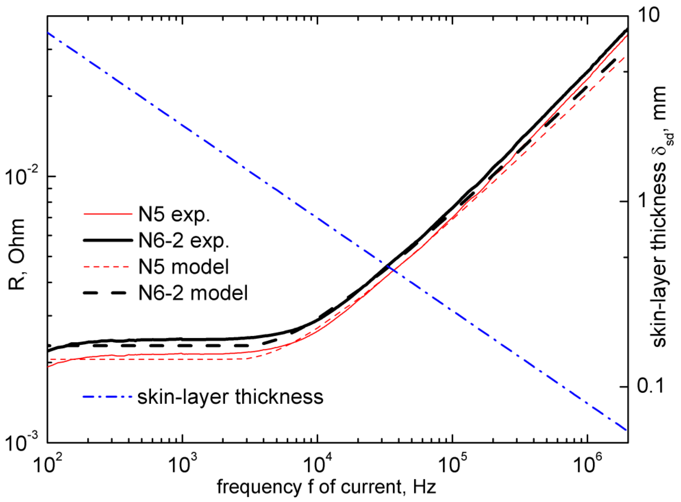
The measurement results are presented in Figure 24. The same Figure gives the thickness of the surface skin layer of an ideal Al conductor with a resistivity ρ = ρAl = 2.62 × 10⁻⁸ Ohm·m, through which the current flows according to Formula (21).
As one can see from Figure 24, the wire after 62 years of operation has a resistance greater than the new wire in the entire frequency range. The most likely reason for this is the thinning of the wire over time during operation or the initially smaller diameter of the wire produced 62 years ago. For wires of both service lives, Figure 24 shows their model resistances, which are simulated by Formulas (21)–(23) when assuming an ideal Al conductor (wire resistivity ρ = ρAl). The deviation of real values from theoretical ones at high frequencies (f > 105 Hz), which is observed even for a new sample, can be associated with a greater influence of the skin effect on the wire resistance in comparison with the model one, for example, due to the initial presence of a damaged layer in a new wire (due to the peculiarities of the process of manufacturing the wires, twisting, oxidation of aluminum, etc.)
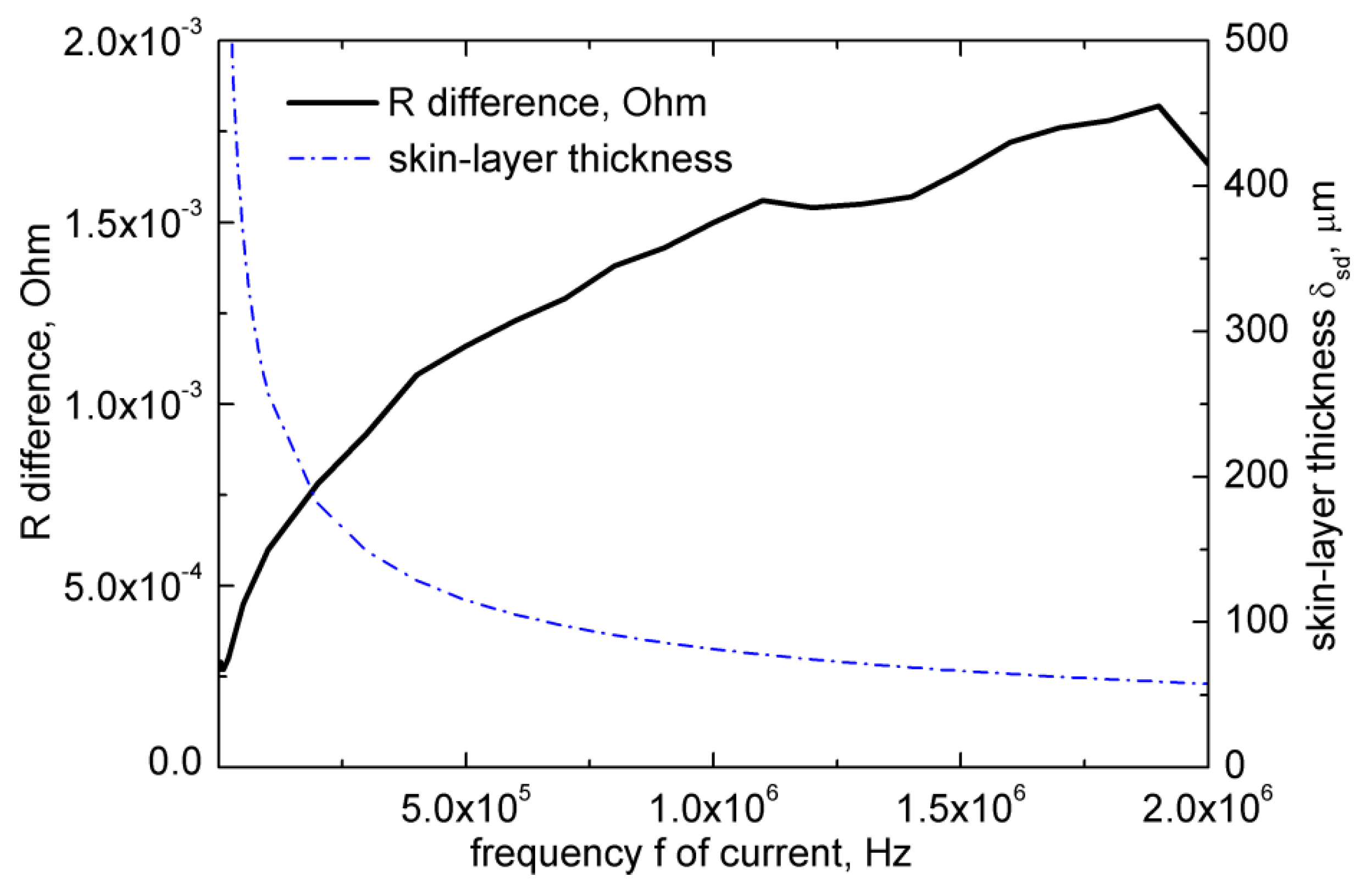
As a demonstration, let us consider the difference between the resistances of the N6-2 and N5 wires on a linear scale in the frequency range from 100 Hz to 2 MHz (Figure 25). It is seen that at low frequencies (up to 2.5 kHz), the difference is less than 0.5 mOhm and increases with increasing frequency. The difference of 70% of the maximum value (i.e., most of the changes in the wire resistance) is achieved at values of the skin-layer thickness δsd of no more than ≈105 μm, which indicates that the largest contribution to the change in resistance after wire operation is induced by microstructure of the wire at a depth from the surface not exceeding ~100 μm. Of course, this is only a rough estimation indicating the order of magnitude of the thickness of the NSDL.
To estimate the depth of the modified layer, a simplified model of the wire-resistance change was built depending on the presence of a modified layer with different thicknesses and different resistivity (it should be noted that the model does not take into account either the possible uneven distribution of the mass density of the modified layer or the possible gradual change in the resistivity from the surface inward). After setting the resistivity ρl and the thickness Tl of the NSDL in the resistance modeling, the total resistance of the wire is calculated, considered as a parallel connection of an ideal Al conductor of the bulk and a conductor with a modified resistivity ρl of the NSDL (see Supplementary Materials, Section S2). Figure 26 presents the corresponding results. The solid black line shows the wire resistance measured experimentally, the black dashed line shows the model for an ideal Al wire with a resistivity ρAl. Models with a damaged outer layer (NSDL) with different resistivity and thickness are shown in different colors and different symbols.
The performed modeling gives an approximate estimation of the possible thickness Tl of the NSDL and its resistivity ρl. However, different combinations of these parameters can lead to similar results of the resistance curve fitting, for example, ρl = 1.2·ρAl at a thickness of Tl = 50 μm, ρl = 1.1·ρAl at a thickness of 90 μm, ρl = 1.075·ρAl at a thickness of Tl = 125 μm, and ρl = 1.05·ρAl at a thickness of Tl = 170 μm.

4. Discussion of Results

Analysis of the data on the study of the defects distribution over the cross-section of aluminum wires, which had been in real operation, has shown that as a result of normal exploitation of wires, there appears the material-surface structure degradation related mainly to the formation of oxides and defects of a void nature.
It is known that the metal-surface layer plays a special role in the crack-incipience process. This layer contains many crystal-structure defects, such as vacancies, dislocations, nano- and micropores, and their clusters. In an alliance, they lead to the appearance of microcracks [44]. A cross-sectional study of wires have shown that the thicknesses of the damaged layer for wire samples after operation, which are determined by various methods, differ significantly. Basically, this result is apparently due to the capabilities of each of the methods.
So, the EBSD mapping has shown no significant changes in the size and shape of the grains in the wires after operation, with the exception of a slight increase in the number of large grains. The geometric parameters (size and shape) of most grains do not change during the service of the wires either inside the wires or near the edges. With an increase in the service life of wires, the formation of a small amount (relative frequency of up to ~1 –3%) of large grains up to ~5 μm (center) and ~6 μm (edge) in the cross section and up to ~10 μm in the longitudinal section (center and edge) is observed. The formation of the larger grains is correlated with increase of the crystallite sizes and development of preferred orientation along [011] Al crystallographic direction as noted in Ref. [9]. These factors may be related to the stretching of wires over time during operation due to sagging, environmental influences, and the influence of electrical voltage. Such microstructural changes during the operation of wires under the influence of either cyclic (vibration) loads or temperature may indicate the occurrence of processes of the dynamic-recrystallization type in the NSDLs [44,45].
Next, according to the densitometric measurements, the NSDL is about 30 μm thick with the strongest decrease in the mass density of the layer, ρdL, at a depth of ~12 μm, the new wire (N5) lacking a NSDL (Figure 17). An increase in the service life leads to an increase in the concentration of void-nature defects mainly at a small near-surface depth of ~12 μm. The value of the density defect ΔρdL/ρdL at a minimum distance from the surface of ~2.5 μm varies from ~0% in the new wire to about −0.4% in the sample N8 after ten years of operation and to −0.75% in the wire N7 with a service life of 18 years, rapidly increasing to values of ΔρdL/ρdL of about −0.1% with distance up to ~12 μm from the surface (in accordance with the exponential-decay law with a negative multiplier). In this case, the total thickness of the defect area (i.e., the total thickness of NSDL) in the samples after operation, defined as the thickness after reaching which the density defect reaches almost zero, does not exceed ~30 μm.
However, analysis of the XRD data on the change in the Al cubic unit-cell parameter has indicated that the thickness of the damaged layer is significantly larger. Similarly to the mass density ρdL of the NSDL of the wire, which is measured by means of the densitometry method experimentally, the calculated value of the X-ray mass density ρx has a minimum value near the surface and increases with inward distance to values in the bulk (again, in accordance with the exponential-decay law with a negative multiplier, but flatter than in the case of mass density ρd obtained by densitometric measurements). In this case, ~70% of the density drop in comparison with the density in the bulk of wires occurs at a depth of ~30 μm for the new sample and ~38 μm for samples after operation, which is in satisfactory agreement with the densitometry data for samples after operation. The magnitude of the density defect Δρx/ρx obtained by XRD is comparable to the ΔρdL/ρdL value found in densitometric measurements, albeit slightly higher in absolute value. For example, the value Δρx/ρx = −1.17%, which is maximum absolute value, was found by XRD from a depth of ~12 μm (i.e., from a part of the NSDL with a thickness of ~12 μm) on sample N7 after 18 years of operation in comparison with ΔρdL/ρdL = −0.75% at a depth of ~2.5 μm for the same sample, as stated above. The same approximately twofold difference is observed for the wire N8 after ten years of operation, respectively, ̶ 0.7% versus ̶ 0.4%. At the same time, in contrast to densitometric measurements, XRD has made it possible to detect the presence of a NSDL in the new sample, although with a much lower density drop Δρx/ρx = −0.17% at the wire surface in comparison with the density in the bulk of the sample.
The approximate value of the thickness of the defect layer, which corresponds to ~99% of the density drop in comparison with the density in the bulk of wire, reaches 56(1) μm for the new sample, increasing almost linearly at a rate of 3.7 μm/year to 96(1) μm and 121(1) μm after 10 (sample N8) and 18 years (N7) of use. The approximate value of the thickness of the defect layer for this sample is estimated to be ~138(1) μm in comparison with 121(1) μm for the sample N7 after 18 years of operation; however, to draw conclusions about the linear nature of the growth of the thickness of this layer and, accordingly, about the slow-down of the growth rate seems to be premature. Further research is needed on specimens with service lives between 18 and 62 years.
The XRD results indicate not only nonlinear distribution of the mass density ρx gradually increasing from the minimum value at the wire surface to the bulk density value, but also a systematic distribution of the microstructure parameters in the NSDL, namely, that of the crystallite sizes D and of the absolute values of microstrains εs in them (Figure 13c,d). The distributions were estimated in the approximation without microstrains (εs = 0) in the case of D as well as in the case of non-zero εs and the D value fixed at the maximum value near the surface. However, as shown in Section 3.4, the estimates remain qualitatively correct, although with the values of D and εs being shifted, respectively, to larger and smaller values at sufficiently large depths from the surface, T > 12 μm. The distribution of crystallite sizes is qualitatively similar to the distribution of Al cubic unit-cell parameters a (cf. Figure 13a,c), and the distribution of the absolute values of microstrains is similar to the distribution of mass densities ρx (cf. Figure 13b,d). Near the surface, the values of a and D are larger, whereas εs and ρx are smaller, nonlinearly decreasing and, respectively, increasing with a retreat from the surface inward. In addition, the D(T) distributions for different samples are rather smooth like a(T) ones. At the same time, in contrast to the smooth nonlinear increase in ρx(T) with the retreat from the surface inward, the microstrain εs, which is characterized by a zero value at depths T~12 μm and less, makes a jump to a nonzero value of ~0.1% (the new wire) to ~0.3% (samples after operation) already at a depth of T~15 μm and remains at this value within e.s.d. at greater depths. A similar jump in the density defect ΔρdL/ρdL from the maximum absolute value to almost zero values was observed in densitometric measurements with an increase in the thickness of the layer removed by etching to ~12 μm. Probably, in both cases, the jump effect is related to an increased content of the void-nature defects in a thin (~12 μm thick) surface layer of wires.
Probably, the heightened concentration of micro-voids, hollows, pores, microcracks, and inclusions directly at the surface, which decreases with distance from the surface, is the main factor influencing the observed density changes described above. Microstructure photographs (Figure 2) obtained using OM methods on the sample N6-2 (service life 62 years) confirm this assumption as well as the performed measurements and calculations. In the wire longitudinal section, according to OM, two characteristic dimensions can be distinguished, which are associated with the subsurface layer. One of them, with a size of ~30 μm, where a large number of defects are concentrated, well correlates with the total size of the defect layer ~30 μm determined in densitometric measurements after layer-by-layer removal of the wire material by etching. In addition, this size satisfactorily correlates with the size of ~38 μm of the occurring ~70% drop value of the density ρx (relative to the density in the bulk of wires) according to XRD estimations. The second characteristic layer size of ~100 μm, where the OM image shows a different structure than in the main part of the wire, is in satisfactory agreement with the approximate size of ~138 μm obtained from XRD calculations.
As the simulations have shown, the electrical resistance at high AC frequencies (more than 0.1 MHz) is also sensitive to the presence of a NSDL with the damaged structure and microstructure due to the presence of the skin effect, i.e., the presence of a skin layer in a conducting sample of a cylindrical shape, in which the current flows. Rough estimates for the difference in electrical resistance of the new wire (N5) and the wire after 62 years of service (N6-2) give a thickness of this layer ~100 μm. However, modeling the electrical resistance of wire N6-2 using two parameters of the NSDL, namely, its thickness and resistivity (which obviously differs from the known resistivity ρAl of an ideal Al material), makes it possible to obtain qualitatively similar experimental and calculated electrical resistivities. For example, when specifying the NSDL resistivity ρ = 1.2·ρAl, the best results are obtained with a layer thickness of ~50 μm, which is close to ~30 μm in densitometric measurements, to ~38 μm in XRD ones (for an estimate corresponding to ~70% of the density drop ρx in comparison with the density in the bulk of wires), and to ~30 μm according to OM. Yet, at a lower resistivity of the NSDL ρ = 1.075·ρAl, which obviously corresponds to a lower concentration of defects in the layer, modeling of the electrical resistivity gives better results for a larger thickness of the near-surface defect layer, namely ~125 μm. This value is in satisfactory agreement with the approximate estimate of the NSDL thickness of ~138 μm from XRD analysis and ~100 μm from OM for the thickness of the entire layer with a changed structure compared to the rest of sample N6-2 (service life of 62 years).
As an illustration, Figure 27 shows the development of a NSDL in investigated wires over time by combining the results of various methods used.
The removal of the NSDL part has been found to lead to a noticeable change in the elastic properties of the material of the samples. The increase in elastic modulus is associated with several factors. First, as is known, the modulus of elasticity is directly proportional to the density of the material. From this point of view, an increase in the modulus of elasticity is due to an increase in the integral density of the sample when the defect layer is removed. Second, according to the theory of internal friction [33], describing the interaction of dislocations with point defects, a decrease in the dislocation density leads to an increase in the Young’s modulus E and a decrease in the decrement δ. That is why the observed changes, namely, an increase in the modulus E and a decrease in the decrement δ, seem to be natural. This effect is especially pronounced for the sample N8 (ten years of service), for which the decrease in the decrement δ after the removal of the NSDL part was more than eleven-fold (Figure 19). The result obtained is an additional confirmation of the significant effect of the defective surface layer on the integral properties of the sample. It can be assumed that just the presence of not only micro-voids (nano- and micropores, microcracks), but also crystal lattice defects of a different kind (dislocations, inclusions, etc.) affect, among other things, the parameters of both the microstructure and structure (in particular, the cubic lattice parameter) more strongly than microcracks. Analysis of the effect on microplastic properties has also shown that an increase in the stress of the microplastic flow σs is observed, with increasing difference before and after surface-layer removal when the amplitude of vibrational strain ε increases.

5. Conclusions

Summing up, the structure and microstructure of the wires from the overhead power-transmission lines operated in the Volgograd region of Russia were investigated. It has been shown that the NSDL exists not only in wires after operation, but also in new wires. The thickness of this defect layer is about 56 μm in the new wire and increases to ~140 μm in a wire after 62 years of service. During the service life from 0 to 18 years, this thickness increases according to a law close to linear, at a rate of ~4 μm/year. In wires after ten years of operation, ~70% of the decrease in the Al-material mass density occurs in the surface layer ~40 μm thick, regardless of the service life. In the new wire, ~70% of the drop in the Al-material mass density is observed in the surface layer ~30 μm thick.
The NSDL is characterized by a systematic nonlinear distribution of properties of both the structure and microstructure of the Al material that makes up this layer. The closer to the surface of this defect layer, the lower its mass density and the larger the parameter of the Al cubic unit-cell of the material forming this layer are. Estimates show an increase in the crystallite sizes when approaching to the surface from ~90 nm for all wires at depth of ~40 μm to ~110–200 nm (depending on the wire service life) near surface and, accordingly, a decrease in microstrains from 0.1–0.3% at the depth to zero near surface (T ≤ 12 μm).
An increase in the service life of wires leads to an increase in the damageability (density of microdefects) of a thin NSDL with a thickness of ~30–40 μm, the highest density being at depths up to ~12 μm from the surface. Depending on the service life of the wires, the distributions of the values of the physical characteristics of the material differ in the amplitude of these distributions (the difference between the maximum and minimum values), which is minimum in the new wire and noticeably grows in the wires after operation. For XRD mass densities taken as an example, the corresponding amplitude is merely 0.17% in the new wire and 1.17% in the wire after 18 years of operation. In the NSDL, microstrains are zero near the surface (T ≤ 12 μm) and sharply increase to ~0.1% in the new wire and to ~0.3% in wires after operation (without damage) at depths from the surface of 15 μm and more. This observation is probably due to the fact that, as mentioned above, the largest number of defects is concentrated at a depth of up to ~12 μm.
The wire after a short circuit shows a relaxation in the distributions of all structure and microstructure characteristics excluding microstrain to practically the values close to those observed at the corresponding depth in the new wire. However, the value of the microstrain (~0.25%) at depths from the surface of 15 μm and more remains close to the value of microstrain in wires that served without damage. The damaged defect area probably extends much deeper in the wire after short circuit than the maximum value of ~140 μm, which is observed in wires that served without short circuits. The structure and thickness of the NSDL in the wire after a short circuit requires further investigation.
All applied research methods have given evidence for the presence of a NSDL, although showing different sensitivity. While EBSD makes it possible to merely determine the existence of a NSDL at a depth of ~100 μm from the surface, the other methods allow one to estimate both the layer thickness and the distribution of defects over the layer. XRD allows one to obtain distributions and estimates of both the total layer thickness (approximate layer thickness where 99% of all changes occur) of ~56–140 μm, and the thickness where most (70%) changes occur, which is ~30–40 μm. OM gives visual estimates of the same thicknesses (~30 μm and ~100 μm, respectively) and do not do it integrally over the entire sample as in XRD experiment, but in local places of the wire cross-section. The densitometric method with layer-by-layer wire material removal is not only sensitive at the layer thickness of ~30 μm, where most (70%) changes occur, but also especially sensible at shallow depths up to ~12 μm. The method of analysis of electrical resistivity makes it possible to obtain both characteristic thicknesses of the NSDL too, although assuming the value of its resistivity (~50 μm at a layer resistivity of 1.2 higher than that of ideal Al, and ~125 μm at a layer resistivity of 1.075 higher).
Since the measurement of electrical resistance is a widely used practice when testing wires, it is possible to control the degree of damage of the wire by detecting the change of the electrical resistance of the near-surface layer. To do this, it is rational to use high frequencies ~3 × 10⁵ Hz-2 × 10⁶ Hz, at which the skin effect is most pronounced, when current flows mainly through a thin layer of the damaged area adjacent to the surface of the conductor.
As for the studied elastic and microplastic properties, it can be concluded that removal of a part of the surface damaged layer ~35 μm thick results in a noticeable increase in both the elastic modulus (from 1.02 to 1.03 times for different samples) and microplastic flow stress (from 1.06 to 4.97 times) and in a decrease in the decrement (from 1.3 to 11.4 times).

Supplementary Materials

The following supporting information can be downloaded at: https://www.mdpi.com/article/10.3390/cryst12020166/s1, Section S1. X-ray diffraction details: Figure S1. Setup of XRD measurements; Figure S2. Scheme of the sample area illuminated by X-rays of an X-ray tube with a linear focus; Figure S3. Examples of XRD reflections (parts of the XRD pattern) measured using sample rotation and without rotation; Figure S4. Scheme for calculation of penetration depth T p e n h k l of X-rays; Figure S5. Distribution along the depth T from the surface of the A50 wire of the mass density ρx(T) of the wire Al material for the sample N7 (service life of 18 years) before and after etching in NaOH. Section S2. Electro resistance measurement and analysis details: Figure S6. Setup of the electro resistance measurement.

Author Contributions

M.V.N., investigation (densitometry, acoustic, OM), methodology, validation, software, writing—original draft preparation; A.A.L., investigation (XRD), methodology, validation, project administration, software, data curation, formal analysis, writing—original draft preparation, writing—review and editing; N.D.P., investigation (electroresistance analysis), software, data curation; writing—original draft preparation; A.I.L., investigation (SEM, EDX, EBSD), methodology, software, writing—original draft preparation; B.K.K., investigation (acoustic), methodology, software; A.G.K., investigation (acoustic), methodology, software; A.G.P., writing—original draft preparation, conceptualization; R.V.S., conceptualization, methodology, project administration; P.N.B., supervision, conceptualization, methodology, funding acquisition; M.M.S., conceptualization, resources (sample acquisition), funding acquisition; V.N.K., conceptualization, resources (sample acquisition); V.N.T., conceptualization, resources (sample acquisition). All authors have read and agreed to the published version of the manuscript.

Funding

This research was funded by the state assignment of Russian Federation No. 0720-2020-0025 “Development of methods and analysis of ways to achieve a high level of safety and competitiveness of objects of energy systems based on digital technologies”.

Data Availability Statement

The data presented in this study are available on request from the corresponding author.

Acknowledgments

The work was carried out using the equipment and software of the Center of Joint Use “Materials Science and Diagnostics in Advanced Technologies” (Ioffe Institute, St. Petersburg, Russia).

Conflicts of Interest

The authors declare no conflict of interest.

Abbreviations

The following abbreviations and nomenclature are used in this manuscript:
AAACAll Aluminum Alloy Conductor
ACSRAluminum Conductor Steel Reinforced
a.m.u.atomic mass unit
CSAscoherent scattering areas
EBSDelectron backscattering diffraction
EDX, EDSenergy-dispersive X-ray microanalysis
e.s.d., e.s.d.s.estimated standard deviation(s)
FWHMfull width at half-maximum of XRD reflection
NSDL, NSDLsdefect near-surface layer(s)
OMoptical Microscopy
PDF-2Powder Diffraction File-2
pVpseudo-Voigt
SEMscanning electron microscopy
SSPsize-strain plot
WHPWilliamson-Hall plot
XLPEcross-linked polyethylene
XRDX-ray diffraction
i.e.,Latin “id est”
etc.Latin “et cetera”
cf.Latin “confer”
2θdiffraction angle
2θBBragg angle of XRD reflection corrected to angular corrections(zero shift and displacement)
2θBobsobserved Bragg andgle of XRD reflection
Artabular value of the atomic mass of aluminium
acubic unit cell parameter
a0parameter of the Al cubic unit cell in the bulk of a new (0 years of service) sample
asatcubic-unit cell parameter of Al material at a depth of Tlayersat
Bintintegral width of XRD reflection
Ca.m.u.conversion factor of a.m.u. into gram
Daverage size of crystallites
Dεs=0mean crystllite size calculated in frame of zero microstrain (εs = 0) model
EYoung’s modulus (modulus of elasticity)
EiYoung’s modulus in the amplitude-independent region
eEuler’s number
FWHMcorrFWHMobs corrected for the instrumental broadening
FWHMinstrinstrumental broadening
FWHMobsobserved full width at half-maximum of XRD reflection
FWHMsizebroadening of reflections due to the size effect of crystallites
FWHMstrainbroadening due to absolute value of microstrain in the crystallite
falternating-current frequency
hklMiller indices
KScherrercoefficient in Scherrer equation
Kstraincoefficient in Wilson-Stokes equation
Imoment of inertia of the sample section
Imaxmaximum intensity of XRD reflection
Iminintegral intensity of XRD reflection
lsample length
msample mass
m0mass of the sample before polishing (etching)
m1mass of piezoelectric quartz
mimass of the sample after polishing of the ith layer
nnumber of harmonics of longitudinal vibrations
Rresistance of the conductor
r0, rradius of the sample (without polishing (etching))
Ssample cross-section
Tdepth from the wire surface
Tetchthickness of the layer removed by polishing (etching)
Tlthickness of the modified (defect) NSL in resistance modeling
Tlayerlayer thickness corresponding to depth where ~70% of the decrease in the mass density ρx occurs in comparison to the ρx200μm value
Tlayersatlayer thickness corresponding to depth where ~99% of the decrease in the mass density ρx occurs in comparison to the ρx200μm value
Toscoscillation period
Tpenpenetration depth of X-ray radiation
T p e n h k l penetration depth of X-ray radiation, corresponding to XRD reflection with Miller indices hkl
vcorcorrosion (defect layer growth) rate
Znumber of formula units in the Al unit cell
γconductivity of the conductor
Δ2θdispldisplacement correction
Δ2θzerocorrecting shift of the zero of the counter
Δa/adefect (relative change) of the unit cell parameter
E/E)hamplitude-dependent Young’s modulus defect (amplitude-dependent variation of E)
Δρd/ρddefect (relative change) of the mass density ρd
ΔρdL/ρdLdensity-defect value of the etched layer
Δρxxdefect (relative change) of the mass density ρx
δlogarithmic decrement of the sample material
δ1logarithmic decrement of the piezoelectric quartz
δ2logarithmic decrement of the piezoquartz-sample system
δhamplitude-dependent part of the logarithmic decrement
δiamplitude-independent part of the logarithmic decrement
δsddepth of skin-layer
εvibrational strain amplitude
εdnon-linear inelastic strain
εsabsolute value of average magnitude of microstrains
εssataverage microstrain εssat in the NSL at depths T ≥ 15 μm, if the crystallite size is fixed and equal to the crystallite size at a depth of T~12 μm
θhalf a diffraction angle
λwavelength
μmagnetic permeability of the conductor material
μ0magnetic permeability of physical vacuum
μlthe mass absorption coefficient of material
μrrelative magnetic permeability of the conductor material
μPPoisson’s ratio of the sample material
ν1frequency of the piezoelectric quartz
ν2frequency of the piezoquartz-sample system
νlindividual frequency of longitudinal vibrations of the rod
ρelectrical resistivity of the conductor
ρAlelectrical resistivity of the aluminium
ρdmass density of material measured by densitometry technique
ρd0density of the sample before polishing (etching) measured by densitometry technique
ρdidensity of the sample after polishing (etching) of the ith layer measured by densitometry technique
ρdLmass density of the etched layer obtained by densitometry technique
ρlresistivity of the modified (defect) NSL
ρxmass density of material calculated according to XRD structural data (XRD mass density)
ρx200μmXRD mass density at depth of 200 μm from the surface estimated from the dependence ρx(T) asscording to exponetial decay law with negative multipier before exponent functiom
ρx500μmsame as ρx200μm but for 500 μm depth from the surface
ρxlayerXRD mass density of Al material at a depth of Tlayer
ρxsatXRD mass density of Al material at a depth of Tlayersat
ρx0XRD density in the bulk of the new (0 years of service) sample
σamplitude of vibrational stress
σsmicroplastic flow stress (micro-flow stress) σs, equal to σ at inelastic strain εd = 5.0 × 10⁻⁸.
Φsecond Euler angle (angle of nutation)
φ1first Euler angle (angle of intrinsic rotation)
φ2third Euler angle (angle of precession)
ωangular frequency of alternating current

References

  1. Papailiou, K.O. (Ed.) Overhead Lines. In Handbook of Power Systems; Springer: Singapore, 2020; pp. 611–758. [Google Scholar] [CrossRef]
  2. Shahid, M.A.; Khan, T.M.; Zafar, Z.; Hashmi, M.F.; Imran, M. Health diagnosis scheme for in-service low voltage Aerial Bundled Cables using super-heterodyned airborne Ultrasonic testing. Electr. Power Syst. Res. 2020, 180, 106162. [Google Scholar] [CrossRef]
  3. Kalombo, R.B.; Martínez, J.M.G.; Ferreira, J.L.A.; da Silva, C.R.M.; Araújo, J.A. Comparative fatigue resistance of overhead conductors made of aluminium and aluminium alloy: Tests and analysis. Proc. Eng. 2015, 133, 223–232. [Google Scholar] [CrossRef] [Green Version]
  4. Araujo, M.M.; Manheimmer, W.A.; Serra, E. Corrosion aspects in aluminum electrical conductors. Mater. Sci. 1988, 8, 175–197. [Google Scholar] [CrossRef]
  5. Karabay, S.; Feyzullahoğlu, E. Determination of early failure sources and mechanisms for Al 99.7% and Al–Mg–Si alloy bare conductors used in aerial transmission lines. Eng. Fail. Anal. 2014, 38, 1–15. [Google Scholar] [CrossRef]
  6. Karabay, S.; Ertürk, A.T.; Zeren, M.; Yamanoğlu, R.; Karakulak, E. Failure analysis of wire-breaks in aluminum conductor production and investigation of early failure reasons for transmission lines. Eng. Fail. Anal. 2018, 83, 47–56. [Google Scholar] [CrossRef]
  7. Azevedo, C.R.F.; Cescon, T. Failure analysis of aluminum cable steel reinforced (ACSR) conductor of the transmission line crossing the Paraná River. Eng. Fail. Anal. 2002, 9, 645–664. [Google Scholar] [CrossRef]
  8. Kreislova, K.; Jaglova, M.; Turek, L.; Koukalova, A. Evaluation of corrosion of long-term exposed aluminium conductor. Koroze Ochr. Mater. 2013, 57, 25–34. [Google Scholar] [CrossRef] [Green Version]
  9. Levin, A.A.; Narykova, M.V.; Lihachev, A.I.; Kardashev, B.K.; Kadomtsev, A.G.; Brunkov, P.N.; Panfilov, A.G.; Prasolov, N.D.; Sultanov, M.M.; Kuryanov, V.N.; et al. Modification of the structural, microstructural, and elastoplastic properties of aluminum wires after operation. Metals 2021, 11, 1955. [Google Scholar] [CrossRef]
  10. Fuente, D.; Otero-Huerta, E.; Morcillo, M. Studies of long-term weathering of aluminium in the atmosphere. Corros. Sci. 2007, 49, 3134–3148. [Google Scholar] [CrossRef]
  11. Yamanaka, S.; Fukuda, T.; Ito, K.; Tomita, J.; Seguchi, T. Use of Residual Voltage for Diagnosis of Electric Power Cables Used in Nuclear Power Stations. Electr. Eng. Jpn. 1997, 119, 18–24. [Google Scholar] [CrossRef]
  12. Humpert, C. Long distance transmission systems for the future electricity supply—Analysis of possibilities and restrictions. Energy 2012, 48, 278–283. [Google Scholar] [CrossRef]
  13. Zhang, Y.; Li, T. Fault location for overhead and cable hybrid transmission lines based on the difference quantities of forward propagating waves and backward propagating waves in HVDC systems. Electr. Power Syst. Res. 2022, 203, 107642. [Google Scholar] [CrossRef]
  14. Han, L.; Zhang, Y.; Li, X.; Jiang, L.; Chen, D. Galloping Reduction of Transmission Lines by Using Phononic Crystal. Crystals 2017, 7, 346. [Google Scholar] [CrossRef] [Green Version]
  15. Brettschneider, S.; Fofana, I. Evolution of Countermeasures against Atmospheric Icing of Power Lines over the Past Four Decades and Their Applications into Field Operations. Energies 2021, 14, 6291. [Google Scholar] [CrossRef]
  16. Lu, J.; Hu, J.; Fang, Z.; Qiao, X.; Zhang, Z. Electric Field Distribution and AC Breakdown Characteristics of Polluted Novel Lightning Protection Insulator under Icing Conditions. Energies 2021, 14, 7493. [Google Scholar] [CrossRef]
  17. Stracqualursi, E.; Araneo, R.; Celozzi, S. The Corona Phenomenon in Overhead Lines: Critical Overview of Most Common and Reliable Available Models. Energies 2021, 14, 6612. [Google Scholar] [CrossRef]
  18. Kul’kov, V.G.; Sultanov, M.M.; Kuryanov, V.N.; Norov, D.S. Electrical reliability simulation based on analysis of fatigue strength of overhead line wires. In Proceedings of the International Youth Conference on Radio Electronics, Electrical and Power Engineering (REEPE), Moscow, Russia, 11–13 March 2021. [Google Scholar] [CrossRef]
  19. Alshwawreh, N.; Alhamarneh, B.; Altwarah, Q.; Quandour, S.; Barghout, S.; Ayasrah, O. Electrical Resistivity and Tensile Strength Relationship in Heat-Treated All Aluminum Alloy Wire Conductors. Materials 2021, 14, 5738. [Google Scholar] [CrossRef]
  20. Xu, X.; Yu, Z.; Li, Y.; Wang, W.; Xu, L. Microstructural Study of Arc Beads in Aluminum Alloy Wires with an Overcurrent Fault. Materials 2021, 14, 4133. [Google Scholar] [CrossRef]
  21. Diffrac. Suite Eva Version 5.1.0.5, Brucker AXS, Karlsruhe, Germany. 2019. Available online: https://www.bruker.com/en/products-and-solutions/diffractometers-and-scattering-systems/x-ray-diffractometers/diffrac-suite-software/diffrac-eva.html (accessed on 28 December 2021).
  22. Fawcett, T.G.; Kabekkodu, S.N.; Blanton, J.R.; Blanton, T.N. Chemical analysis by diffraction: The Powder Diffraction File™. Powder Diffr. 2017, 32, 63–71. [Google Scholar] [CrossRef]
  23. Topas Version 5, Technical reference. Brucker AXS, Karlsruhe, Germany. 2014. Available online: https://www.bruker.com/en/products-and-solutions/diffractometers-and-scattering-systems/x-ray-diffractometers/diffrac-suite-software/diffrac-topas.html (accessed on 28 December 2021).
  24. O’Connor, B.H.; Li, D.Y.; Hunter, B.A. The importance of the specimen displacement correction in Rietveld pattern fitting with symmetric reflection-optics diffraction data. Adv. X-ray Anal. 2001, 44, 96–102. [Google Scholar]
  25. Welzel, U.; Ligot, J.; Lamparter, P.; Vermeulen, A.C.; Mittemeijer, E.J. Stress analysis of polycrystalline thin films and surface regions by X-ray diffraction. J. Appl. Crystallogr. 2005, 38, 1–29. [Google Scholar] [CrossRef]
  26. Terlan, B.; Levin, A.A.; Börrnert, F.; Simon, F.; Oschatz, M.; Schmidt, M.; Cardoso-Gil, R.; Lorenz, T.; Baburin, I.A.; Joswig, J.-O.; et al. Effect of Surface Properties on the Microstructure, Thermal, and Colloidal Stability of VB2 Nanoparticles. Chem. Mater. 2015, 27, 5106–5115. [Google Scholar] [CrossRef]
  27. Terlan, B.; Levin, A.A.; Börrnert, F.; Zeisner, J.; Kataev, V.; Schmidt, M.; Eychmüller, A. A Size-Dependent Analysis of the Structural, Surface, Colloidal, and Thermal Properties of Ti1−xB2 (x = 0.03 − 0.08) Nanoparticles. Eur. J. Inorg. Chem. 2016, 2016, 3460–3468. [Google Scholar] [CrossRef]
  28. Langford, J.I. A Rapid Method for Analysing the Breadths of Diffraction and Spectral Lines using the Voigt Function. J. Appl. Cryst. 1978, 11, 10–14. [Google Scholar] [CrossRef]
  29. Scherrer, P. Bestimmung der Grösse und der inneren Struktur von Kolloidteilchen mittels Röntgenstrahlen. Nachr. Königl. Ges. Wiss. Göttingen. 1918, 26, 98–100. (In German) [Google Scholar]
  30. Rehani, B.R.; Joshi, P.B.; Lad, K.N.; Pratap, A. Crystallite size estimation of elemental and composite silver nano-powders using XRD principles. Indian J. Pure Appl. Phys. 2006, 44, 157–161. [Google Scholar]
  31. Halder, N.C.; Wagner, C.N.J. Separation of particle size and lattice strain in integral breadth measurements. Acta Cryst. 1966, 20, 312–313. [Google Scholar] [CrossRef]
  32. Stokes, A.R.; Wilson, A.J.C. The diffraction of X-rays by distorted crystal aggregates. Proc. Phys. Soc. 1944, 56, 174–181. [Google Scholar] [CrossRef]
  33. Nikanorov, S.P.; Kardashev, B.K. Elasticity and Dislocation Inelasticity of Crystals; Nauka: Moscow, Russia, 1985; p. 254. (In Russian) [Google Scholar]
  34. Chernov, V.M.; Kardashev, B.K.; Krjukova, L.M.; Mamaev, L.I.; Plaksin, O.A.; Rusanov, A.E.; Solonin, M.I.; Stepanov, V.A.; Votinov, S.N.; Zavialski, L.P. Internal friction and anelastic properties of vanadium and V ̶ Ti ̶ Cr alloys. J. Nucl. Mater. 1998, 257, 263–273. [Google Scholar] [CrossRef]
  35. Faria, J.A.M.B.; Raven, M.S. On the success of electromagnetic analytical approaches to full time-domain formulation of skin effect phenomena. Progr. Electromagn. Res. M 2013, 31, 29–43. [Google Scholar] [CrossRef] [Green Version]
  36. Raven, M.S. Experimental measurements of the skin effect and internal inductance at low frequencies. Acta Tech. 2015, 60, 51–69. [Google Scholar]
  37. Wyslouch, B.; Wecht, B.; Knuteson, B.; Katsavounidis, E.; Roland, R.; Belcher, J.; Formaggio, J.; Dourmashkin, P.; Simcoe, R. Chapter 6. Current and Resistance. In 8.02 Physics II: Electricity and Magnetism; Spring 2007; MIT Open Course Ware, Massachusetts Institute of Technology: Cambridge, MA, USA, 2007. [Google Scholar]
  38. Mason, J.K.; Schuh, C.A. Representation of Texture. In Electron Backscatter Diffraction in Material Science, 2nd ed.; Schwartz, A.I., Kumar, M., Adams, B.L., Field, D.P., Eds.; Springer: Boston, MA, USA, 2009; pp. 45–46. [Google Scholar] [CrossRef]
  39. ·Tsybulya, S.; Kryukova, G. New X-ray powder diffraction data on δ-Al2O3. Powder Diffr. 2003, 18, 309–311. [Google Scholar] [CrossRef]
  40. Fargeot, D.; Mercurio, D.; Dauger, A. Structural characterization of alumina metastable phases in plasma sprayed deposits. Mater. Chem. Phys. 1990, 24, 299. [Google Scholar] [CrossRef]
  41. Chaim, R.; Hefetz, M. Effect of grain size on elastic modulus and hardness of nanocrystalline ZrO2-3 wt.% Y2O3 ceramic. J. Mater. Sci. 2004, 39, 3057–3061. [Google Scholar] [CrossRef]
  42. Kardashev, B.K.; Betekhtin, V.I.; Narykova, M.V. Elastoplastic properties of micro and submicrocrystalline metals and alloys. Tech. Phys. 2015, 60, 1829–1841. [Google Scholar] [CrossRef]
  43. Gremaud, G. Dislocation—Point defect interactions. Mat. Sci. Forum. 2001, 366–368, 178–246. [Google Scholar] [CrossRef]
  44. Jurkiewicz, B.; Smyrak, B.; Zasadzińska, M.; Franczak, K.; Strzępek, P. The researches of influence of strengthening on fatigue strength of aluminium wires for OHL conductors. Arch. Civ. Mech. Eng. 2019, 19, 862–870. [Google Scholar] [CrossRef]
  45. Gourdet, S.; Montheillet, F. A Model of Continuous Dynamic Recrystallization. Acta Mater. 2003, 51, 2685–2699. [Google Scholar] [CrossRef]
Figure 1. OM images. (a) Typical microcrack on the surface of sample N6-2 (service life 62 years), (b) crack in the NSDL of a longitudinal section of sample N7 (service life 18 years). The dark area is the technological substrate.
Crystals 12 00166 g001
Figure 2. OM image of the sample N6-2 (62 years of service). Longitudinal section with a visible damaged layer (NSDL). The dark area is the technological substrate.
Crystals 12 00166 g002
Figure 3. Maps of the distribution of Euler angles for cross-sections of samples: (a) new (N5), at the edge and (b) after 10 years of service (N8), at the edge. The legend shown in (c) is the same for (a) and (b). Scales for Euler angles Φ and φ2 are the same.
Crystals 12 00166 g003
Figure 4. Maps of the distribution of Euler angles for cross-sections of samples: (a) new (N5), at the edge, (b) after 10 years of service (N8), at the center and (c) after 10 years of service (N8), at the edge. The legend shown in (d) is the same for (ac). Scales for Euler angles Φ and φ2 are the same.
Crystals 12 00166 g004
Figure 5. Histograms of grain size distribution for cross-sections of samples: (a) new (N5), at the center (from [9]) and at the edge, (b) after 10 years of service (N8), in the center (from [9]) and at the edge.
Crystals 12 00166 g005
Figure 6. Histograms of grain size distribution for longitudinal sections of samples: (a) new (N5), at the center and at the edge, (b) after 10 years of service (N8), in the center and at the edge.
Crystals 12 00166 g006
Figure 7. Histograms of grain aspect ratio distribution for cross-sections of samples: (a) new (N5), at the center (from [9]) and at the edge, (b) after 10 years of service (N8), in the center (from [9]) and at the edge.
Crystals 12 00166 g007
Figure 8. Histograms of grain aspect ratio distribution for longitudinal sections of samples: (a) new (N5), at the center and at the edge, (b) after 10 years of service (N8), in the center and at the edge.
Crystals 12 00166 g008
Figure 9. Histograms of grain-boundary misorientation-angle distribution for sample cross-sections: (a) new (N5), at the center (from [9]) and at the edge, (b) after 10 years of service (N8), in the center (from [9]) and at the edge.
Crystals 12 00166 g009
Figure 10. Histograms of grain-boundary misorientation-angle distribution for longitudinal sections of samples: (a) new (N5), at the center and at the edge, (b) after 10 years of service (N8), in the center and at the edge.
Crystals 12 00166 g010
Figure 11. XRD patterns of samples N5-2, new (a) and N6-2, service life of 62 years (b). The Miller indices hkl attributed to Al phase and service life duration of the samples are indicated. The observed reflections attributed to δ- and/or δ*-Al2O3 and their Miller indices are shown in (b) using different symbols.
Crystals 12 00166 g011
Figure 12. X-ray radiation penetration depths Tpen into the Al wire for the observed reflections of Al XRD patterns of the A50-type samples N5-2 (new) and N7 (18 years of service) depending on the diffraction angle 2θ. The diffraction angles 2θ at which the reflections are observed correspond to their Bragg angles 2θB, 2θ = 2θB.
Crystals 12 00166 g012
Figure 13. Distribution along the depth T from the surface of the A50 wire of (a) the cubic unit-cell parameter a of the wire Al material, (b) the mass density ρx(T) of the wire Al material, (c) the size D of crystallites in the model without microstrains (εs = 0), and (d) the microstrain εs estimated under the assumption of a fixed crystallite size equal to the crystallite size near the surface (at a depth of T~12 μm). Samples are numbered according to Table 1 and their lifetimes are shown in (a,c,d). At the right sides of (a,b), the axes are shown corresponding, respectively, to the estimates of the lattice defect Δa/a and the density defect Δρx/ρx, which are estimated with respect to the bulk of the new sample (0 years of operation). The lines in (a,b,c) are drawn according to the exponential-decay law. In (a,b), the thicknesses Tlayer of the NSDL are estimated from the intersection of distribution curves for samples of different service life with a curve corresponding to a new sample. The inset in (b) presents the extrapolations of the distribution curves to depths of 200 μm from the surface for samples that served without damage. The shown estimates of the total thickness Tlayersat of the NSDL for wires that served without damage for the whole time are obtained from the intersection with tangents drawn at the points when the distribution curves reach a plateau (when ρx reaches the value ρxsat = 99.99% of the density estimated from the distribution curve at a depth of 200 μm). The inset in (d) shows an example of estimation of the average microstrain εssat in the NSDL at depths T ≥ 15 μm, if the crystallite size is fixed and equal to the crystallite size at a depth of T~12 μm.
Crystals 12 00166 g013aCrystals 12 00166 g013b
Figure 14. The thicknesses Tlayer and Tlayersat obtained, respectively, from the intersection of the approximation dependences ρx(T) with ρx(T) of the new sample and with the tangent to the plateau of the approximation dependences ρx(T) (drawn at the points when ρx reaches the value ρxsat = 99.99% of the density ρx200μm estimated from the distribution curve ρx(T) at a depth of 200 μm) as dependences on the service life of the Al wires of overhead power lines of the A50 type. Lines are a guide to the eye only.
Crystals 12 00166 g014
Figure 15. Mass density ρxsat equal to 99.99% of the density ρx200μm estimated from the distribution curve ρx(T) at a depth of 200 μm, and the corresponding value of the Al-material cubic unit-cell parameter asat versus the service life of the wires of overhead power lines of type A50. Lines are a guide to the eye only.
Crystals 12 00166 g015
Figure 16. Microstrain εssat calculated under the assumption of a fixed crystallite size equal to the crystallite size near the surface (at a depth of T~12 μm) depending on the service life of the Al wires of the overhead power lines of A50 type (AAAC, without steel core). For comparison, the values of microstrain εs obtained by the SSP method in [9] are shown, corresponding to the values of the microstrain averaged over the entire experimentally achieved X-ray penetration depth of ~36 μm.
Crystals 12 00166 g016
Figure 17. The dependence of the density-defect ΔρdL/ρdL value in the near-surface layer of wires on the thickness Tetch of the layer removed by etching for samples N5 (0 years old), N8 (service life of 10 years), and N7 (service life of 18 years).
Crystals 12 00166 g017
Figure 18. Strain amplitude dependences of Young’s modulus E and decrement δ for new wire N5 before (5) and after (5′) etching. Measurements were performed at room temperature.
Crystals 12 00166 g018
Figure 19. Strain amplitude dependences of Young’s modulus E and decrement δ for wire N8 after ten years of operation before (8) and after (8′) etching. Measurements were performed at room temperature.
Crystals 12 00166 g019
Figure 20. Strain amplitude dependences of Young’s modulus E and decrement δ for wire N7 after ten years of operation before (7) and after (7′) etching. Measurements were performed at room temperature.
Crystals 12 00166 g020
Figure 21. Diagrams of microplastic strain of Al samples (new wire N5) before (5) and after (5′) etching.
Crystals 12 00166 g021
Figure 22. Diagrams of microplastic strain of Al samples (wire N8 after 10 years of operation) before (8) and after (8′) etching.
Crystals 12 00166 g022
Figure 23. Diagrams of microplastic strain of Al samples (wire N7 after 18 years of operation) before (7) and after (7′) etching.
Crystals 12 00166 g023
Figure 24. AC resistances of wires N5 (new) and N6-2 (62 years of service) depending on the frequency f of the current. The experimental curves of electrical resistance are shown by solid lines of different colors and thickness. Dashed and dotted lines of the same color and smaller thickness show the model curves of electrical resistance, which are simulated under the assumption of an ideal Al conductor. The blue dash-dotted line is the calculated thickness δsd of the current-carrying skin layer in the case of an ideal Al conductor.
Crystals 12 00166 g024
Figure 25. Difference of resistances N6-2 (service life 62 years) and N5 (0 years) measured at frequencies from 100 Hz to 2 MHz. The blue dash-dotted line is the calculated thickness δsd of the current-carrying skin layer in the case of an ideal Al conductor.
Crystals 12 00166 g025
Figure 26. Resistance of the wire N6-2 (service life 62 years) in the high-frequency range f = 1× 10⁵–2·× 106 Hz of the dependence. The model of the resistance of an ideal Al wire without a NSDL is shown with a dashed line and symbols in the form of solid black squares. Resistivity models with different sets of values of resistivity ρl and thickness Tl of NSDL are shown with different symbols in different colors. The blue dash-dotted line is the calculated thickness δsd of the current-carrying skin layer in the case of an ideal Al conductor. The inset shows the enlarged area in the 1.05–1.25 MHz range, which is indicated in the figure by a rectangle.
Crystals 12 00166 g026
Figure 27. Development of a NSDL in A50 wires over time of exploitation in overhead power lines.
Crystals 12 00166 g027
Table 1. Samples of wires of overhead power lines with different service life, which were selected for research.
Sample NTypeService Life, YearsDamage
5-2A500No
5AC500No
8A5010No
7A5018No
3A5035After short circuit
6-2A5062No
Table 2. Density ρd according to the results of densitometric measurements, Young’s modulus E, amplitude-independent decrement δi, and micro-flow stress σs = σ at inelastic strain εd = 5.0 × 10⁻⁸.
Sample NService Life t, Yearsρd, g/cm3E, GPaδi, 10−5σs, MPa
502.694971.82716.2
5′0 73.21717.1
8102.690669.44573.3
8′10 71.44016.4
7182.690571.2859.8
7′18 72.4689.8
Publisher’s Note: MDPI stays neutral with regard to jurisdictional claims in published maps and institutional affiliations.