Article

Electrical and Structural Properties of CVD-Graphene Oxidized Using KMnO4/H2SO4 Solution

1
Department of Advanced Materials Science and Engineering, Kumoh National Institute of Technology, Gumi 39177, Korea
2
Advanced Materials Research Center, Kumoh National Institute of Technology, Gumi 39177, Korea
*
Author to whom correspondence should be addressed.
Crystals 2022, 12(4), 439; https://doi.org/10.3390/cryst12040439
Submission received: 4 March 2022 / Revised: 14 March 2022 / Accepted: 18 March 2022 / Published: 22 March 2022

Abstract

:
We report the electrical properties of graphene grown via chemical vapor deposition (CVD-graphene) and oxidized using a KMnO4/dilute H2SO4 mixture. CVD-graphene was successfully oxidized without any pores or peeling off from the substrates. When the H2SO4 concentration was increased, the electrical resistance of the oxidized graphene (OG) increased. In particular, OG-20 shows a nonlinear current–voltage curve similar to that of a diode owing to direct tunneling through the interfaces between the nanosized sp2 and sp3 regions. The changes in electrical properties occurred because of structural evolution. As the H2SO4 concentration increased, the number of oxygen functional groups (epoxide/hydroxyl and carboxyl groups) in the OG increased. In addition, a reduction in the average distance between defects in the OG was determined using Raman spectroscopy. Oxidation using a KMnO4/dilute H2SO4 mixture results in CVD-graphene with modified electrical properties for graphene-based applications.

1. Introduction

The chemical functionalization of a graphene surface can easily modify its electrical, chemical, and optical properties. In particular, oxygen functionalization offers metal–insulator transition by controlling the degree of oxidation, reaction sites for the synthesis of other functional groups, and a route for hole doping [1,2]. Thus far, considerable research has been devoted to controlling the metal–insulator transition by manipulating the degree of oxidation through the partial oxidation and reduction of graphene oxide. Jin et al. reported that oxidized graphene (OG) field-effect transistors (FETs) show p-type characteristics for partial oxidation (for 5 min) and insulating behavior for full oxidation (for 60 min) of graphene in air [2]. Goki et al. reported a carrier transport mechanism in partially oxidized graphene (POG) synthesized by varying the reduction time of graphene oxide [3]. They demonstrated that carrier transport in lightly reduced graphene oxide occurs via variable-range hopping, whereas band-like transport dominates in well-reduced graphene oxide. Carrier transport in graphene oxide is intriguing because of the presence of the substantial electronic disorder arising from variable sp2 and sp3 carbon ratios. Graphene oxide represents graphene layers with oxygen functional groups decorated on the basal planes and edges. In graphene oxide, most of the carbon atoms bonded with oxygen are sp3 hybridized and disrupt the extended sp2 conjugated network of the original graphene sheet. The substantial sp3 fraction in graphene oxide can transform the material into a semiconductor and ultimately to a graphene-like semimetal.
Although a large number of studies have been devoted to the synthesis of graphene oxide via chemical exfoliation using graphite flakes, such as Hummer’s method, there is limited availability of mass-production processes for graphene oxide for electronic applications because graphene oxide is a micro-sized sheet [4,5]. Graphene oxide sheets cannot form uniform and large-area films. Graphene grown via chemical vapor deposition (CVD-graphene) has the following advantages: (i) it is easy to achieve the scalable production of graphene suitable for the mass production of graphene-based electronic devices; and (ii) it can form monocrystalline and polycrystalline graphene [6,7,8,9]. In addition, it can be patterned using conventional lithography techniques and can be transferred onto flexible substrates with negligible structural damage.
To oxidize the CVD-graphene, many studies have been conducted using dry oxidation methods, such as ozone treatment assisted by UV irradiation and oxygen plasma treatment [10,11,12,13]. However, these dry oxidation methods can easily form nanoscale pits (or pores) in the graphene [14,15,16]. In contrast, wet-based chemical oxidation of CVD-graphene has rarely been reported. The wet oxidation of CVD-graphene offers several advantages, such as a low-cost process, a wide range of solvents that can be used, and easy control of the metal-insulator transition through the adjustment of the oxidation time [2,17].
In this study, we demonstrate the variation in electrical properties and structural evolution of oxidized CVD-graphene using the reagents used in Hummers’ method, which is a mixed solution of KMnO4 and H2SO4. The electrical properties of the oxidized CVD-graphene were evaluated using current–voltage (I-V) plots, as a function of the H2SO4 concentration, and by calculating the Schottky barrier height (SBH, Φb) and the gate bias effect. The electrical properties were dependent on the structural properties of OG, which were investigated using scanning electron microscopy (SEM), X-ray photoelectron spectroscopy (XPS), and Raman spectroscopy.

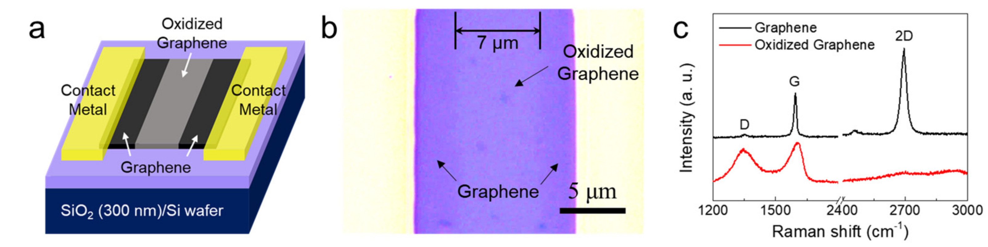
2. Materials and Methods

Graphene layers were grown on Cu foils using a thermal CVD method. The detailed growth procedure was as follows: (1) initial step at 5 mTorr and 1000 °C under 10 sccm of Ar gas for 1 h; (2) annealing at 1000 °C under Ar 10 sccm/H2 50 sccm atmosphere for 20 min; (3) graphene growth step at 1000 °C under Ar 10 sccm/H2 50 sccm/CH4 50 sccm for 1 min; and (4) final step at room temperature (25 °C) under an Ar/H2/CH4 atmosphere. For the transfer of graphene onto SiO2/Si wafers, graphene grown on the other surface of Cu foils was first removed by O2 plasma (SPI supplies, Plasma Prep III) at 100 W for 10 s. Subsequently, the graphene/Cu foil samples were coated with poly methyl methacrylate (PMMA). After the Cu foils were etched in a 0.5 M ammonium persulfate solution, the PMMA/graphene samples were floated on deionized water. Finally, the PMMA/graphene samples were transferred onto SiO2/Si wafers, and the PMMA was removed by immersion in acetone for 1 h.
To measure the electrical properties, the mesa isolation of the graphene sheet with a dimension of 25 × 50 μm2 was conducted using O2 plasma treatment. Subsequently, Pd/Au (20 nm/50 nm) metal layers as ohmic contacts and an Au (50 nm) metal pad as an external contact were deposited using an electron-beam evaporator. The distance between the two electrodes was 13 μm. A surface oxidation region with a length of 7 μm was defined using photolithography.
The surface oxidation of graphene was performed using 0.1 g of KMnO4 in a 10–30% dilute H2SO4 mixture. The graphene transferred onto a SiO2/Si wafer was immersed in the KMnO4/dilute H2SO4 mixture for 10 min at 25 °C. Graphene oxidized with different concentrations of H2SO4 is denoted as OG-n, where n represents the H2SO4 concentration. Finally, the graphene on the SiO2/Si wafer was immersed in DI water for 1 min and cleaned by N2 blowing.
Optical microscopy (OM) and field-effect scanning electron microscopy (FE-SEM) were used to characterize the graphene layer transferred onto the SiO2/Si wafer. High resolution transmission electron microscopy (HRTEM) was utilized to investigate the surface of the samples. The chemical bonds of the oxygen functional groups of the samples were investigated using XPS with a Theta Probe AR-XPS system (Thermo Fisher Scientific, Waltham, MA, USA) with the following parameters: monochromatic Al Kα radiation (hν = 1486.6 eV), X-ray energy of 15 kV, 150 W, and a spot size of 400 μm2. Micro Raman spectroscopy (System 1000, Renishaw, Wotton-under-Edge, UK) with a 514 nm diode laser was used to analyze the structural variation of the OG structures. OM objective lenses (×100 magnification) were used to acquire the Raman spectra. The spectral resolution of the equipment is 1800 l/mm gratings. The electrical characteristics of the OG structures were investigated based on DC characteristics using a system combined with HP4156C (Keysight, Santa Rosa, CA, USA) and a probe station.

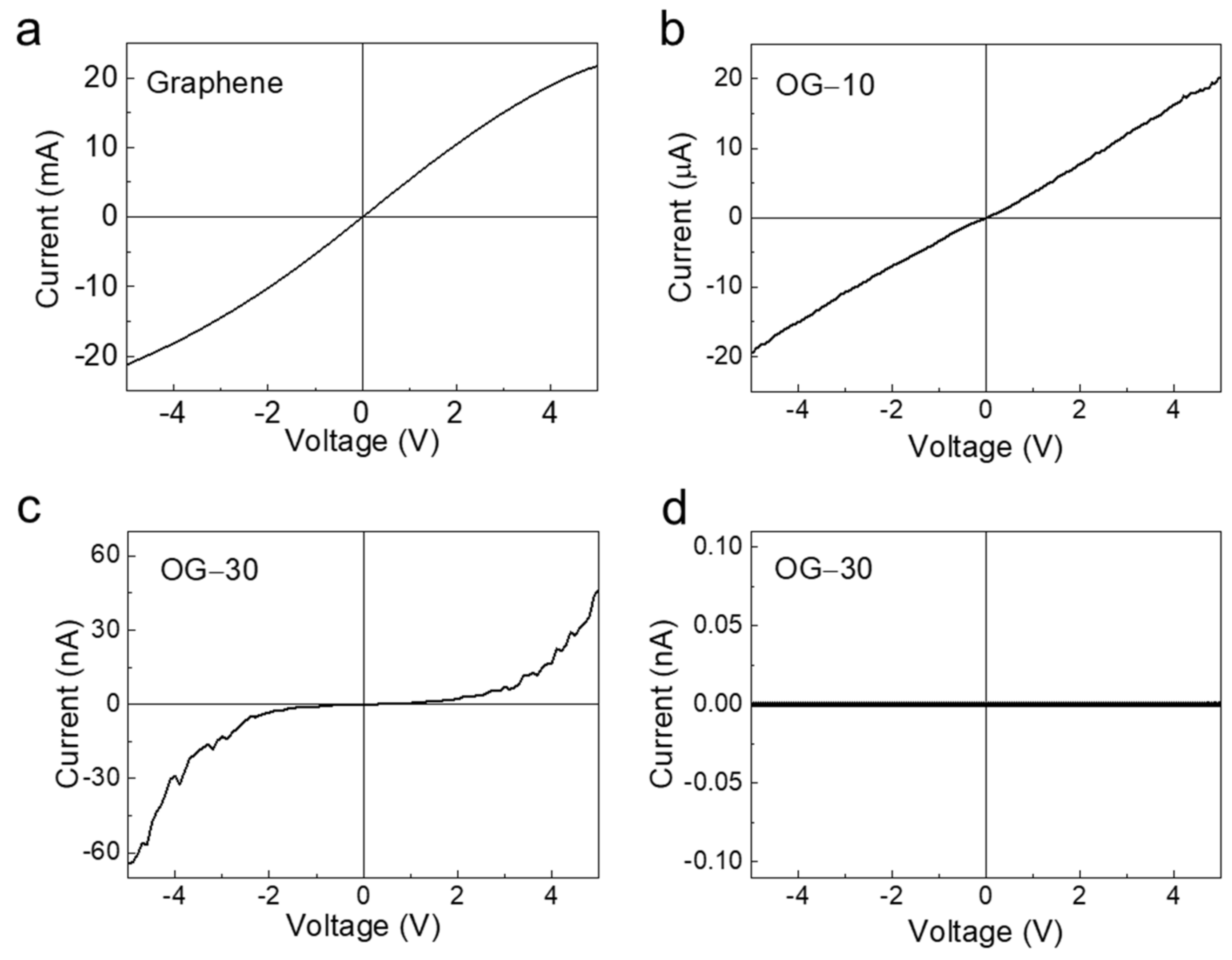
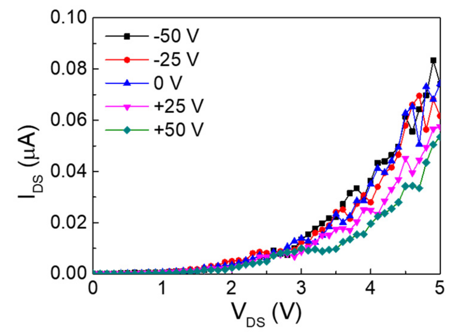
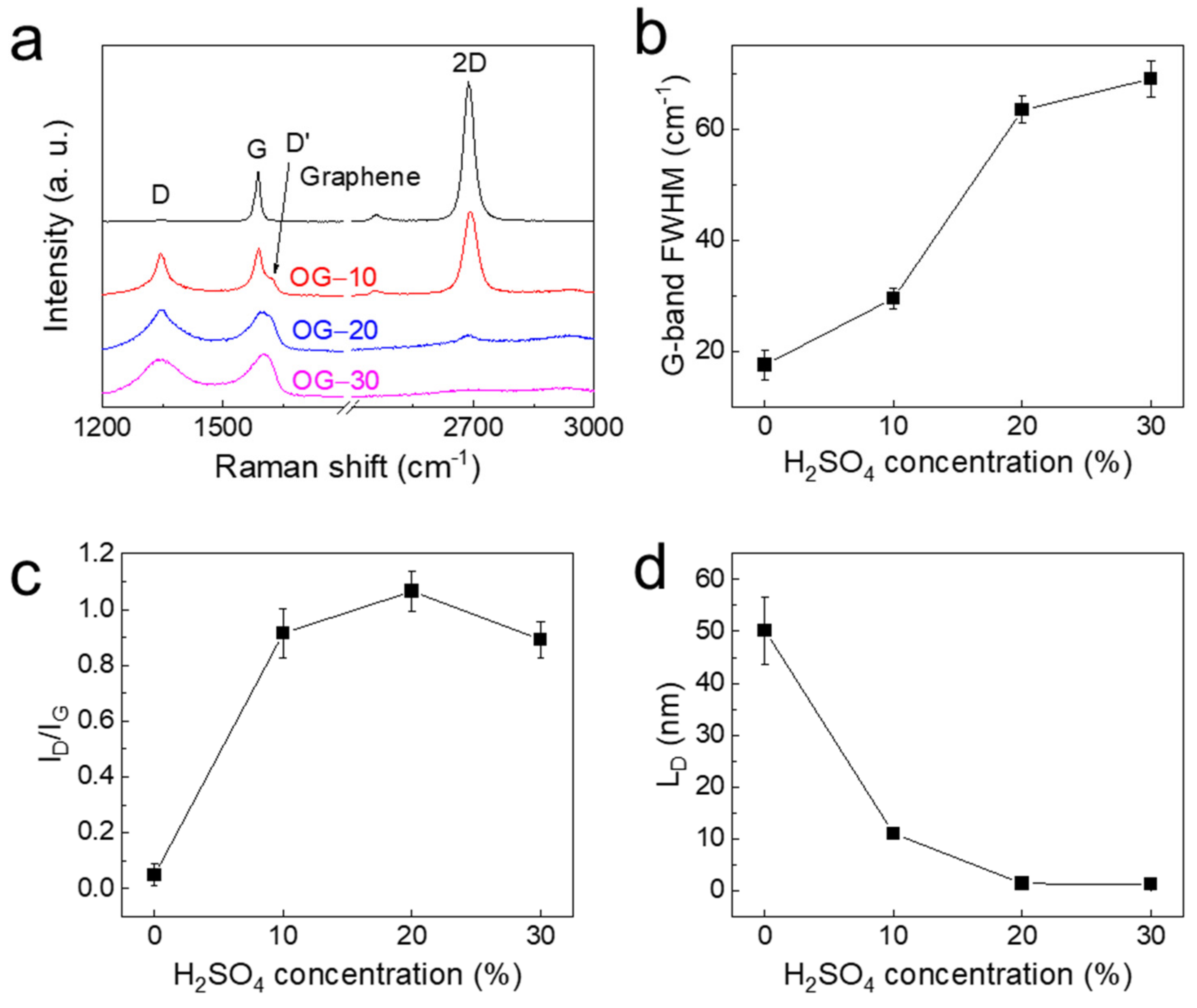
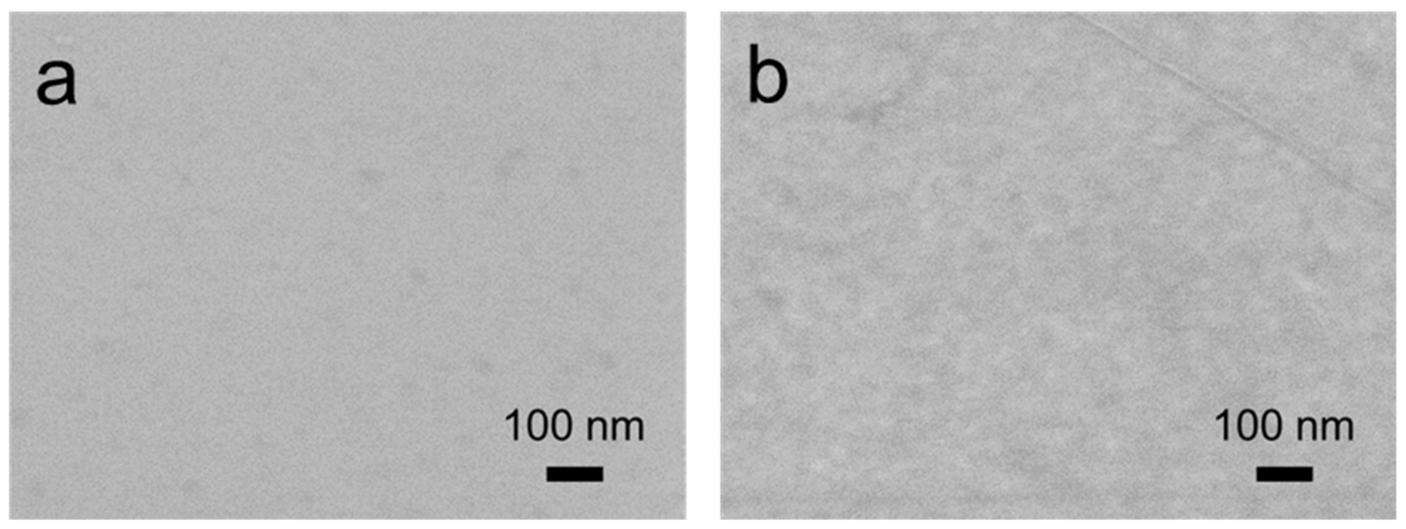
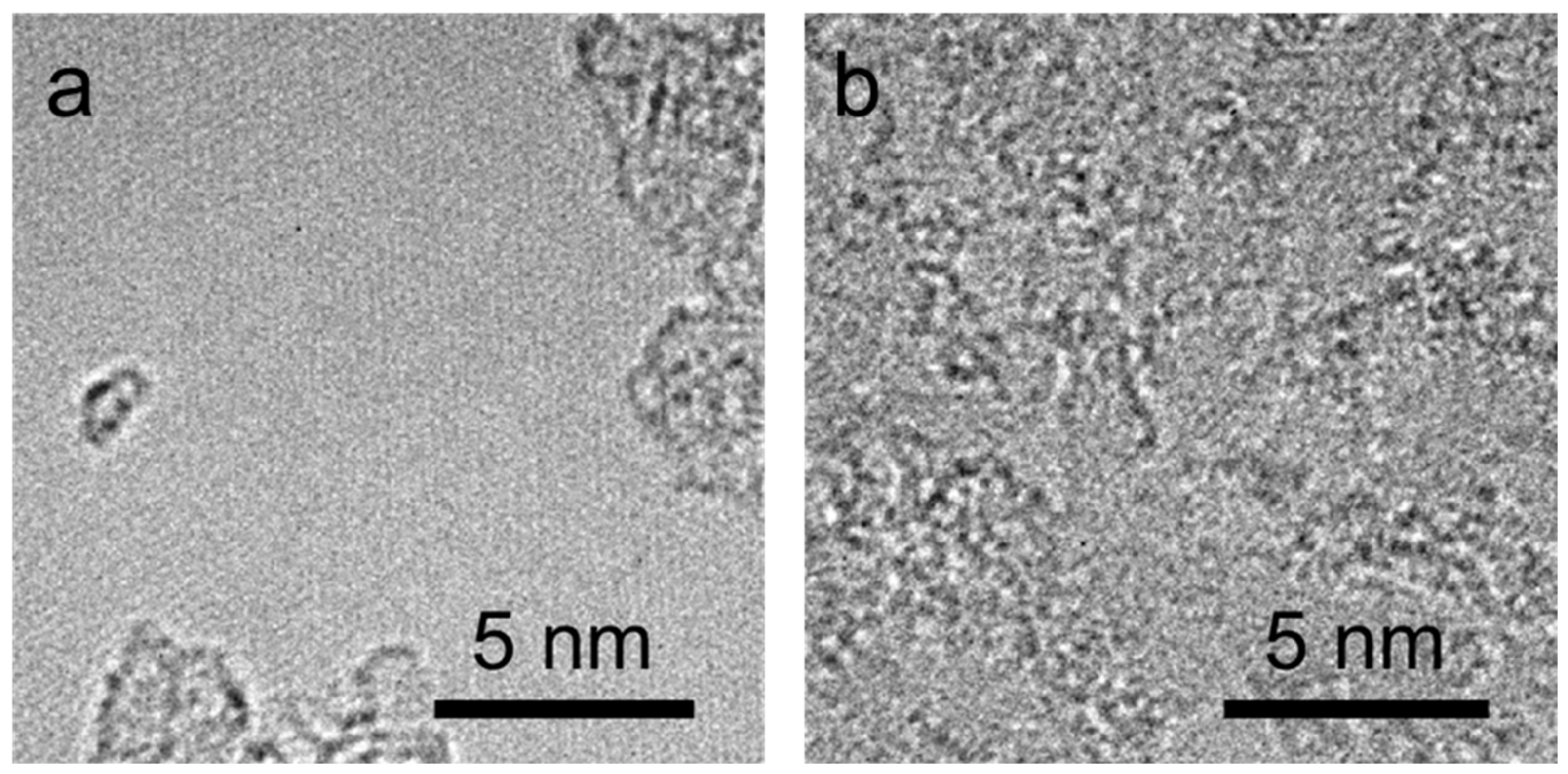
3. Results and Discussion

Figure 1a presents a schematic of the graphene/OG in-plane heterostructure used to evaluate the electrical properties. OG regions were formed using conventional photolithography. The length of the OG region is 7 µm, as shown in Figure 1b. From the OM image, the OG region has a lighter color than graphene, possibly because of the oxygen functional groups on the OG [18]. The Raman spectra shown in Figure 1c indicate the formation of OG regions after oxidation using KMnO4/H2SO4 solution. The detailed structural changes in the OG are discussed later using XPS and Raman analyses as a function of the H2SO4 concentration.
Current–voltage (I-V) curves of graphene/OG-10, OG-20, or OG-30 in-plane heterostructures were obtained. As shown in Figure 2a,b, OG-10 displays a resistance approximately 100 times higher than that of graphene. The I-V plot for OG-20 is a nonlinear curve, which is different from that of OG-10 (Figure 2c). The I-V curve of the graphene/OG-20 structure is similar to that of graphene/graphene oxide vertical contact structures [19]. The OG-30 acts as an insulator, as shown in Figure 2d. Figure 3 shows the IDS-VDS curves as a function of the gate voltage. The OG-20 shows p-type behavior. This is due to the presence of oxygen functional groups on the surface and/or edges of graphene [20].
Assuming an ideal diode without shunt and series resistances, the SBH of the graphene/OG-20 in-plane heterostructure can be calculated by employing a thermionic model, using the following Equation (1):
Φ b = k T q ln A T 2 A I 0
where k is the Boltzmann constant; T is the absolute temperature; q is the electronic charge; A is the contact area of the barrier; A* is the Richardson constant (119.7 A·cm–2·K–2 for a free electron); and I0 is the saturation current obtained from the I-V curves. The estimated SBH for OG-20 was 0.28 eV.
To demonstrate the change in electrical properties of oxidized CVD-graphene as a function of the H2SO4 concentration, we investigated the structural evolution using XPS and Raman analyses. Figure 4 shows the C1s spectra of graphene, OG-10, OG-20, and OG-30. The graphene (Figure 4b) spectrum indicates the presence of strong C–C bonds, a low amount of epoxide (C–O–C)/hydroxyl (C–OH) groups, and a very small amount of carboxyl groups (O–C=O), at 284.6, 285.4, and 288.7 eV, respectively [21]. In the OG-10 spectrum, the amount of epoxide/hydroxyl and carboxyl groups is slightly higher than that in the graphene. Significantly, the peak intensities corresponding to the oxygen functional groups in OG-20 are significantly higher than those in OG-10 (Figure 4d). In addition, when the H2SO4 concentration was increased further (OG-30), the number of epoxide/hydroxyl groups increased slightly more than that in OG-20. The peak intensity ratio (IOC/IGC) of oxidized carbon (285.4, 288.7, and 291 eV) to graphitic carbon (284.6 eV) explains the oxidation degree of graphene oxide [10,22]. The IOC/IGC values of graphene, OG-10, OG-20, and OG-30 were calculated as 0.24, 0.3, 0.6, and 0.84, respectively (see Table 1). Therefore, the increase in the amount of oxygen functional groups changes the shape of the I-V curve from linear (graphene and OG-10) to nonlinear (OG-20).
Figure 5a shows the Raman spectra of graphene, OG-10, OG-20, and OG-30. The graphene spectrum shows sharp G- and 2D-bands at 1587.5 and 2688.9 cm−1, with full width at half maximum (FWHM) values of 17.8 and 33.9 cm−1, respectively, whereas a negligible D-band is observed at approximately 1340 cm−1. In the OG-10 spectrum, D- and D’-bands (1625 cm−1), which are associated with defects in graphene, appear, and the 2D-band intensity is slightly decreased compared to that of the graphene [23,24]. The defects in the OG-10 are due to vacancies, physical adsorption of oxygen-related molecules, and oxygen functional groups, including epoxide/hydroxyl, carbonyl, and carboxyl groups [22]. Compared with the OG-10, the FWHM of the G-band of OG-20 increases from 29.6 cm−1 (OG-10) to 63.4 cm−1 (OG-20) as shown in Figure 5b. Moreover, the 2D-band intensity is significantly reduced in OG-20.
The average distance between defects (LD) in the OG can be calculated approximately using the intensity ratio of D- to G-bands (ID/IG) [25,26]. Ferrari and co-workers proposed a three-stage classification of the disorder of graphitic materials from graphite to amorphous carbon using Raman spectroscopy [24,27]. The first is from graphite to nanocrystalline graphite; the second is from nanocrystalline graphite to low sp3 amorphous carbon, and the third is from low sp3 amorphous carbon to high sp3 amorphous carbon. To calculate the LD of the graphene and OG specimens, we considered the following results of previous studies [28]. First, from graphene to graphene oxide, the ID/IG values initially increased (stage 1) and then decreased (stage 2). Second, the OG in stages 1 and 2 can have similar ID/IG values, while the LD decreases. Finally, the FWHM of the G-band increases with an increase in defects; therefore, the ID/IG value and FWHM of the G-band must be considered simultaneously because of much larger values in stage 2. Figure 5c plots ID/IG versus the H2SO4 concentration (0% H2SO4 indicates graphene). The ID/IG values of OG specimens changed from 0.04 for graphene to 0.843 for OG-10, 1.06 for OG-20, and 0.878 for OG-30. Therefore, the ID/IG value increases from graphene to OG-20, but the value for OG-30 is similar to that of OG-10. In addition, the G-band FWHM of OG-20 was significantly higher than that of OG-10. Considering the above results, graphene and OG-10 are stage 1 graphitic materials, and OG-20 and OG-30 are stage 2 materials. The LD values of graphene and OG specimens were calculated to be 49.28 (graphene), 11.04 (OG-10), 1.387 (OG-20), and 1.263 nm (OG-30), as shown in Figure 5d. These results indicate that the change in the electrical properties is due to the formation of oxygen functional groups, leading to the structural disorder.
The phenomenon of carrier transport in the graphene/OG-20 in-plane heterostructure can be explained using the Mott variable-range hopping (VRH) model, which involves consecutive inelastic tunneling processes between localized states [29,30,31,32]. Perhaps, OG-20 is composed of nano-sized sp2 domains and a sp3 matrix (disordered region), which is confirmed by the calculated LD values as shown in Figure 5, and the disordered region plays a role as a transport barrier at the interface [32]. As shown in Figure 6, the FE-SEM image of OG-20 shows some heterogeneity in contrast, whereas the graphene appears relatively uniform. This is because of the difference in the electrical resistance between the graphene and OG-20 regions [10]. Moreover, HRTEM images (Figure 7) present the different surface morphologies of graphene and OG-20. The OG-20 has a smaller grain size than that of the graphene. The results verify the increase in the disordered regions in OG-20. The oxygen functional groups form discontinuous localized states below the conduction band, which play an important role in trapping the electrical carriers and scattering during transport. The direct tunneling of carriers through the interface between the sp2 and sp3 domains reveals a nonlinear I-V curve in OG-20. Therefore, it is confirmed that the electrical properties of the graphene/OG-20 in-plane heterostructures changed to a nonlinear curve with an SBH of 0.28 eV, owing to the many structural variations created by the oxygen functional groups in OG-20.

4. Conclusions

In summary, we demonstrated variations in the electrical properties of CVD-graphene oxidized using different amounts of KMnO4/H2SO4. The degree of oxidation of the OG specimens can be simply controlled by varying the H2SO4 concentration. When the H2SO4 concentration is above 20%, the graphene/OG in-plane heterostructure exhibits a nonlinear curve. The SBH of OG-20 was calculated to be 0.28 eV. Charge carrier transport in our devices was due to direct tunneling through interfaces between nanosized sp2 and sp3 regions. The sp3 regions are formed by oxygen functional groups on the graphene surface. As a result, our simple oxidation technique enabled the modification of the electrical properties of CVD-graphene. Furthermore, the electrical characteristics of the graphene/OG in-plane heterostructures allow the design of functionalized graphene-based applications with in-plane heterostructures.

Author Contributions

Writing—original draft preparation, J.-S.C., K.-S.I. and S.-J.A.; investigation, J.-S.C., T.-K.L. and Y.-J.C.; synthesis, J.-S.C. and T.-K.L.; fabrication, J.-S.C. and K.-S.I. All authors have read and agreed to the published version of the manuscript.

Funding

This research received no external funding.

Institutional Review Board Statement

Not applicable.

Informed Consent Statement

Not applicable.

Data Availability Statement

Not applicable.

Acknowledgments

This work was supported by Kumoh National Institute of Technology.

Conflicts of Interest

The authors declare no conflict of interest.

References

  1. Lonkar, S.P.; Deshmukh, Y.S.; Abdala, A.A. Recent advances in chemical modifications of graphene. Nano Res. 2015, 8, 1039–1074. [Google Scholar] [CrossRef]
  2. Jin, M.; Jeong, H.-K.; Yu, W.J.; Bae, D.J.; Kang, B.R.; Lee, Y.H. Graphene oxide thin film field effect transistors without reduction. J. Phys. D. Appl. Phys. 2009, 42, 135109. [Google Scholar] [CrossRef]
  3. Eda, G.; Ball, J.; Mattevi, C.; Acik, M.; Artiglia, L.; Granozzi, G.; Chabal, Y.; Anthopoulos, T.D.; Chhowalla, M. Partially oxidized graphene as a precursor to graphene. J. Mater. Chem. 2011, 21, 11217–11223. [Google Scholar] [CrossRef]
  4. Jiříčková, A.; Jankovský, O.; Sofer, Z.; Sedmidubský, D. Synthesis and applications of graphene oxide. Materials 2022, 15, 920. [Google Scholar] [CrossRef] [PubMed]
  5. Suhaimin, N.S.; Hanifah, M.F.R.; Azhar, M.; Jaafar, J.; Aziz, M.; Ismail, A.F.; Othman, M.H.D.; Rahman, M.A.; Aziz, F.; Yusof, N.; et al. The evolution of oxygen-functional groups of graphene oxide as a function of oxidation degree. Mater. Chem. Phys. 2022, 278, 125629. [Google Scholar] [CrossRef]
  6. Bae, S.; Kim, H.; Lee, Y.; Xu, X.; Park, J.-S.; Zheng, Y.; Balakrishnan, J.; Lei, T.; Ri Kim, H.; Il Song, Y.; et al. Roll-to-roll production of 30-inch graphene films for transparent electrodes. Nat. Nanotechnol. 2010, 5, 574–578. [Google Scholar] [CrossRef] [PubMed] [Green Version]
  7. Lee, Y.-C.; Lee, H.U.; Lee, K.; Kim, B.; Lee, S.Y.; Choi, M.-H.; Farooq, W.; Choi, J.S.; Park, J.-Y.; Lee, J.; et al. Aminoclay-conjugated TiO2 synthesis for simultaneous harvesting and wet-disruption of oleaginous Chlorella sp. Chem. Eng. J. 2014, 245, 143–149. [Google Scholar] [CrossRef]
  8. Zhou, H.; Yu, W.J.; Liu, L.; Cheng, R.; Chen, Y.; Huang, X.; Liu, Y.; Wang, Y.; Huang, Y.; Duan, X. Chemical vapour deposition growth of large single crystals of monolayer and bilayer graphene. Nat. Commun. 2013, 4, 2096. [Google Scholar] [CrossRef] [Green Version]
  9. Yan, Z.; Lin, J.; Peng, Z.; Sun, Z.; Zhu, Y.; Li, L.; Xiang, C.; Samuel, E.L.; Kittrell, C.; Tour, J.M. Toward the synthesis of wafer-scale single-crystal graphene on copper foils. ACS Nano 2012, 6, 9110–9117. [Google Scholar] [CrossRef]
  10. Islam, A.E.; Kim, S.S.; Rao, R.; Ngo, Y.; Jiang, J.; Nikolaev, P.; Naik, R.; Pachter, R.; Boeckl, J.; Maruyama, B. Photo-thermal oxidation of single layer graphene. RSC Adv. 2016, 6, 42545–42553. [Google Scholar] [CrossRef]
  11. Yuan, J.; Ma, L.-P.; Pei, S.; Du, J.; Su, Y.; Ren, W.; Cheng, H.-M. Tuning the electrical and optical properties of graphene by ozone treatment for patterning monolithic transparent electrodes. ACS Nano 2013, 7, 4233–4241. [Google Scholar] [CrossRef]
  12. Aria, A.I.; Gani, A.W.; Gharib, M. Effect of dry oxidation on the energy gap and chemical composition of CVD graphene on nickel. Appl. Surf. Sci. 2014, 293, 1–11. [Google Scholar] [CrossRef]
  13. Mao, H.; Wang, R.; Zhong, J.; Zhong, S.; Chen, W. Mildly O2 plasma treated CVD graphene as a promising platform for molecular sensing. Carbon N. Y. 2014, 76, 212–219. [Google Scholar] [CrossRef]
  14. Liu, L.; Ryu, S.; Tomasik, M.R.; Stolyarova, E.; Jung, N.; Hybertsen, M.S.; Steigerwald, M.L.; Brus, L.E.; Flynn, G.W. Graphene oxidation: Thickness-dependent etching and strong chemical doping. Nano Lett. 2008, 8, 1965–1970. [Google Scholar] [CrossRef] [Green Version]
  15. Zandiatashbar, A.; Lee, G.-H.; An, S.J.; Lee, S.; Mathew, N.; Terrones, M.; Hayashi, T.; Picu, C.R.; Hone, J.; Koratkar, N. Effect of defects on the intrinsic strength and stiffness of graphene. Nat. Commun. 2014, 5, 3186. [Google Scholar] [CrossRef] [PubMed]
  16. Kim, D.C.; Jeon, D.-Y.; Chung, H.-J.; Woo, Y.; Shin, J.K.; Seo, S. The structural and electrical evolution of graphene by oxygen plasma-induced disorder. Nanotechnology 2009, 20, 375703. [Google Scholar] [CrossRef]
  17. Dreyer, D.R.; Park, S.; Bielawski, C.W.; Ruoff, R.S. The chemistry of graphene oxide. Chem. Soc. Rev. 2010, 39, 228–240. [Google Scholar] [CrossRef]
  18. Jia, S.; Sun, H.D.; Du, J.H.; Zhang, Z.K.; Zhang, D.D.; Ma, L.P.; Chen, J.S.; Ma, D.G.; Cheng, H.M.; Ren, W.C. Graphene oxide/graphene vertical heterostructure electrodes for highly efficient and flexible organic light emitting diodes. Nanoscale 2016, 8, 10714–10723. [Google Scholar] [CrossRef] [PubMed]
  19. Wu, X.; Sprinkle, M.; Li, X.; Ming, F.; Berger, C.; de Heer, W.A. Epitaxial-graphene/graphene-oxide junction: An essential step towards epitaxial graphene electronics. Phys. Rev. Lett. 2008, 101, 26801. [Google Scholar] [CrossRef] [Green Version]
  20. Piazza, A.; Giannazzo, F.; Buscarino, G.; Fisichella, G.; La Magna, A.; Roccaforte, F.; Cannas, M.; Gelardi, F.M.; Agnello, S. Effect of air on oxygen p-doped graphene on SiO2. Phys. Status Solidi 2016, 213, 2341–2344. [Google Scholar] [CrossRef]
  21. Yang, D.; Velamakanni, A.; Bozoklu, G.; Park, S.; Stoller, M.; Piner, R.D.; Stankovich, S.; Jung, I.; Field, D.A.; Ventrice, C.A.; et al. Chemical analysis of graphene oxide films after heat and chemical treatments by X-ray photoelectron and Micro-Raman spectroscopy. Carbon N. Y. 2009, 47, 145–152. [Google Scholar] [CrossRef]
  22. Chen, J.; Zhang, Y.; Zhang, M.; Yao, B.; Li, Y.; Huang, L.; Li, C.; Shi, G. Water-enhanced oxidation of graphite to graphene oxide with controlled species of oxygenated groups. Chem. Sci. 2016, 7, 1874–1881. [Google Scholar] [CrossRef] [Green Version]
  23. Kaniyoor, A.; Ramaprabhu, S. A Raman spectroscopic investigation of graphite oxide derived graphene. AIP Adv. 2012, 2, 32183. [Google Scholar] [CrossRef] [Green Version]
  24. Ferrari, A.C. Raman spectroscopy of graphene and graphite: Disorder, electron–phonon coupling, doping and nonadiabatic effects. Solid State Commun. 2007, 143, 47–57. [Google Scholar] [CrossRef]
  25. Tuinstra, F.; Koenig, J.L. Raman spectrum of graphite. J. Chem. Phys. 1970, 53, 1126–1130. [Google Scholar] [CrossRef] [Green Version]
  26. Lucchese, M.M.; Stavale, F.; Ferreira, E.H.M.; Vilani, C.; Moutinho, M.V.O.; Capaz, R.B.; Achete, C.A.; Jorio, A. Quantifying ion-induced defects and Raman relaxation length in graphene. Carbon N. Y. 2010, 48, 1592–1597. [Google Scholar] [CrossRef]
  27. Ferrari, A.C.; Robertson, J. Interpretation of Raman spectra of disordered and amorphous carbon. Phys. Rev. B 2000, 61, 14095–14107. [Google Scholar] [CrossRef] [Green Version]
  28. Ferrari, A.C.; Basko, D.M. Raman spectroscopy as a versatile tool for studying the properties of graphene. Nat. Nanotechnol. 2013, 8, 235–246. [Google Scholar] [CrossRef] [Green Version]
  29. Gómez-Navarro, C.; Weitz, R.T.; Bittner, A.M.; Scolari, M.; Mews, A.; Burghard, M.; Kern, K. Electronic transport properties of individual chemically reduced graphene oxide sheets. Nano Lett. 2007, 7, 3499–3503. [Google Scholar] [CrossRef]
  30. Hill, R.M. Hopping conduction in amorphous solids. Philos. Mag. A J. Theor. Exp. Appl. Phys. 1971, 24, 1307–1325. [Google Scholar] [CrossRef]
  31. Mott, N.F. Conduction in non-crystalline materials. Philos. Mag. A J. Theor. Exp. Appl. Phys. 1969, 19, 835–852. [Google Scholar] [CrossRef]
  32. Sun, Y.; Kirimoto, K.; Hattori, H.; Kitamura, Y.; Fan, E.; Onishi, K. Electric field and oxygen concentration-dependent transport properties of nano-graphene oxide. AIP Adv. 2019, 9, 95010. [Google Scholar] [CrossRef]
Figure 1. (a) Schematic and (b) OM image of the graphene/OG heterostructure; and (c) Raman spectra of the graphene and OG-30.
Crystals 12 00439 g001
Figure 2. Current-voltage (I-V) curves of (a) graphene, (b) OG-10, (c) OG-20, and (d) OG-30.
Crystals 12 00439 g002
Figure 3. IDS-VDS measurements of the OG-20 as a function of gate-bias voltages.
Crystals 12 00439 g003
Figure 4. (a) XPS C 1s spectra of graphene and OG samples as a function of the H2SO4 concentration. Detailed peak analyses of (b) graphene, (c) OG-10, (d) OG-20, and (e) OG-30.
Crystals 12 00439 g004
Figure 5. (a) Raman spectra, (b) G-band FWHM, (c) ID/IG, and (d) average distance between defects (LD) of graphene and OGs as a function of the H2SO4 concentration.
Crystals 12 00439 g005
Figure 6. FE-SEM images of (a) graphene and (b) OG-20.
Crystals 12 00439 g006
Figure 7. HRTEM images of (a) graphene and (b) OG-20.
Crystals 12 00439 g007
Table 1. Intensity ratio of the oxidized carbon and graphitic carbon (IOC/IGC) as a function of the H2SO4 concentration.
Chemical BondsGrapheneOG-10OG-20OG-30
Graphitic carbon (%)80.3877.0662.5954.33
Oxidized carbon (%)19.6222.9437.4145.67
IOC/IGC0.240.300.600.84
Publisher’s Note: MDPI stays neutral with regard to jurisdictional claims in published maps and institutional affiliations.

