Abstract
In this work, the correlation between SiO2 deposition thickness and hydrogen content is discussed and the effect of the SiO2 layer on the properties of synaptic InGaZnO (IGZO) TFTs is analyzed. Three types of IGZO synaptic thin-film transistors (TFTs) were fabricated with different gate insulators, and the effect of SiO2 as a gate insulator was investigated. XPS analysis confirmed that the hydrogen content in the Al2O3 and SiO2 layers increased during SiO2 deposition step for all depth regions. Hydrogen injected by the SiO2 layer deposition step was confirmed to improve the memory window through more threshold voltage shift under positive bias stress (PBS) and negative bias stress (NBS) conditions. In addition, the retention characteristics were improved due to the low hydrogen movement velocity in the SiO2 layer. These results contribute to the optimization of the amount of hydrogen, and the proposed device has potential as a synaptic device capable of neuromorphic computing.
1. Introduction
It is necessary to efficiently process a large amount of data as advanced technologies related with artificial intelligence such as autonomous vehicles have recently approached to our lives. In the case of conventional von Neumann computing systems including central processing units, a bottleneck occurs when processing a large amount of data due to a serial computation and a physically separated structure between the memory and the processor [1]. Neuromorphic systems are enabled to perform vector-by-matrix-multiplication (VMM) operations in parallel using Ohm’s law and Kirchhoff’s law, which enables low-power and high-efficient in-memory computing [2,3,4,5,6,7,8]. Therefore, it is important to investigate synaptic devices suitable for neuromorphic systems in artificial neuromorphic computing systems.
Recently, in addition to two-terminal synaptic devices such as resistive switching memory [9,10,11,12,13,14,15,16] and phase change memory [17,18,19,20], three-terminal synaptic devices are also receiving great attention because input and output ports can be used independently [21,22,23,24,25,26,27,28,29]. Among them, InGaZnO (IGZO) thin-film transistors (TFTs) has good compatibility with conventional processes and can be utilized as a nonvolatile memory. It is also widely used especially in flexible applications and displays thanks to its low-temperature processing, uniformity, low-leakage current and high mobility [30,31,32,33,34]. Therefore, it is necessary to verify the synaptic properties by integrating IGZO TFTs on a flexible substrate using a low-temperature process.
In this study, we fabricated three types of synaptic IGZO TFTs (single Al2O3 layer and double stack layers Al2O3/SiO2 with SiO2 thickness of 5 nm and 10 nm, respectively) on flexible substrates using different stacks of gate insulators. The devices threshold voltage (VT) modulation can be achieved under positive gate bias stress (PBS) and negative gate bias stress (NBS) due to the movement of hydrogen ions in the Al2O3 layer deposited by low-temperature (LT) atomic layer deposition (ALD). In addition, X-ray photoelectron spectroscopy (XPS) analysis and electrical measurement demonstrated that the SiO2 layer deposited by e-beam evaporation was a source of additional hydrogen ions and improved the memory window. Lastly, it was confirmed that the SiO2 layer contributed to the improvement of retention by controlling the movement velocity of hydrogen ions.
2. Materials and Methods
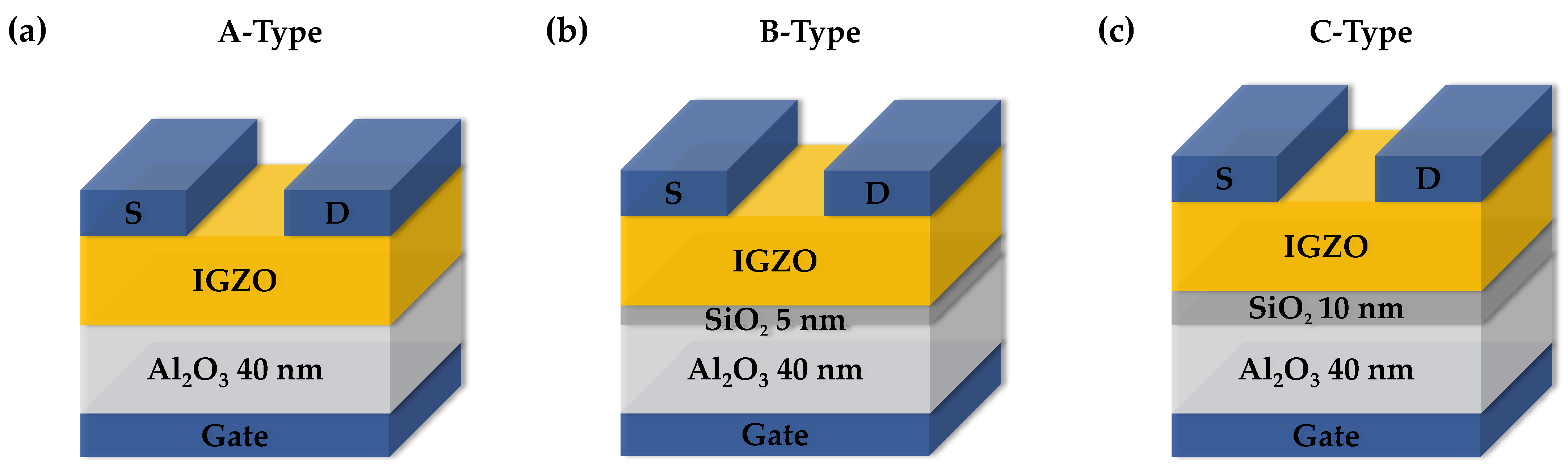
Three types of IGZO TFTs were fabricated on a polyethylene terephthalate (PET)/SiO2/p+-Si substrate with varying the gate dielectric stack as show in Figure 1a–c. Except the gate insulator deposition, A-type (Al2O3 layer), B-type (Al2O3/SiO2 5 nm) and C-type (Al2O3/SiO2 10 nm) devices share the whole process flow. First, A PET film was cleaned with acetone in a sonicator. On the PET substrate, 50-nm-thick SiO2 layer was deposited using an e-beam evaporator as a buffer layer. The gate layer was deposited with 20 nm-thick Cu and patterned by e-beam evaporation and lift-off, respectively. The single layer (without SiO2) of Al2O3 (40 nm) and double layer of Al2O3 (40 nm)/SiO2 (5 and 10 nm) were subsequently deposited by LT ALD (Al2O3 layer) with Al(CH3)3 and H2O as reactant vapor at 80℃ and e-beam evaporator (SiO2 layer), respectively. Then, 35-nm-thick IGZO layer was deposited at a room temperature with an active layer shadow mask by reactive sputtering (3(Ar)/0.1(O2) sccm, 5 mTorr, 150 W RT power). The source and drain regions were formed with 40-nm-thick Cu deposited by an e-beam evaporator followed by lift-off. Finally, the devices were annealed in air for 1 h at 250 °C in the air condition for detaching PET substrate from the silicon substrate. The channel width and length of the devices were defined as 50 and 20 μm, respectively.
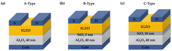
Figure 1.
Schematic view of three-type bottom gate IGZO TFTs. (a) LT ALD-deposited 40 nm Al2O3 (A-type), (b) LT ALD 40 nm Al2O3/e-beam 5 nm SiO2 (B-type) and (c) 10 nm SiO2 (C-type).
3. Results
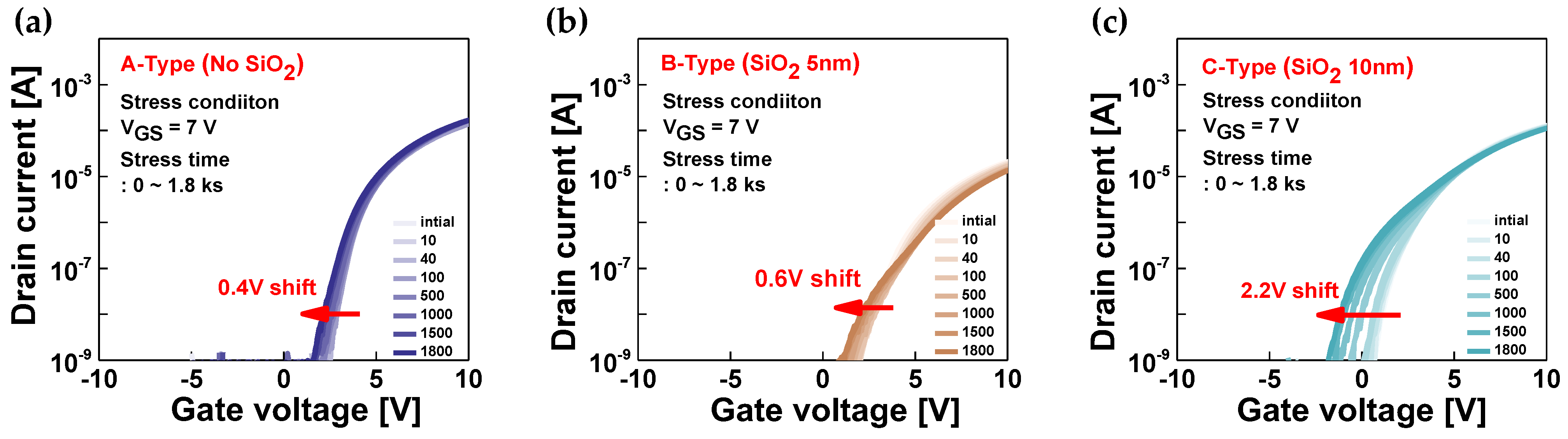
Figure 2a–c show the I-V characteristics of three types of IGZO TFTs under PBS condition at gate voltage (VGS) = 7 V. As the PBS time increases, the three types of IGZO TFTs show a negative VT shift of 0.4, 0.6, and 2.2 V, respectively. The thicker the SiO2 layer is, the larger VT shift is obtained. In our previous study, the VT modulation of IGZO TFT was determined by the migration of hydrogen ions inside Al2O3 layer [35,36]. In addition, when additional SiO2 layer was deposited as a gate insulator on the Al2O3 layer, a larger VT shift was obtained under PBS because additional SiO2 deposition step helps to generate additional hydrogen by dissociating the Al-H bonds in Al2O3 layer. In our previous study, it was confirmed that the hydrogen content was much higher when the SiO2 layer was deposited on the Al2O3 than when deposited without the Al2O3 layer [37]. This implies that the insertion of an additional SiO2 layer acts as a hydrogen source, and the amount of hydrogen depends on the thickness of the SiO2 layer. Additional hydrogen ions moving toward the IGZO channel under the PBS help to form an inversion layer of the IGZO channel and increase the amount of negative VT shift since hydrogen acts as an n-type dopant [38,39].
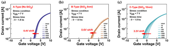
Figure 2.
I-V characteristics of (a) A-type, (b) B-type, and (c) C-type IGZO TFTs under a positive bias stress (PBS). When the thickness of the SiO2 layer is sufficiently wide, a significant threshold voltage shift occurs in the PBS condition.
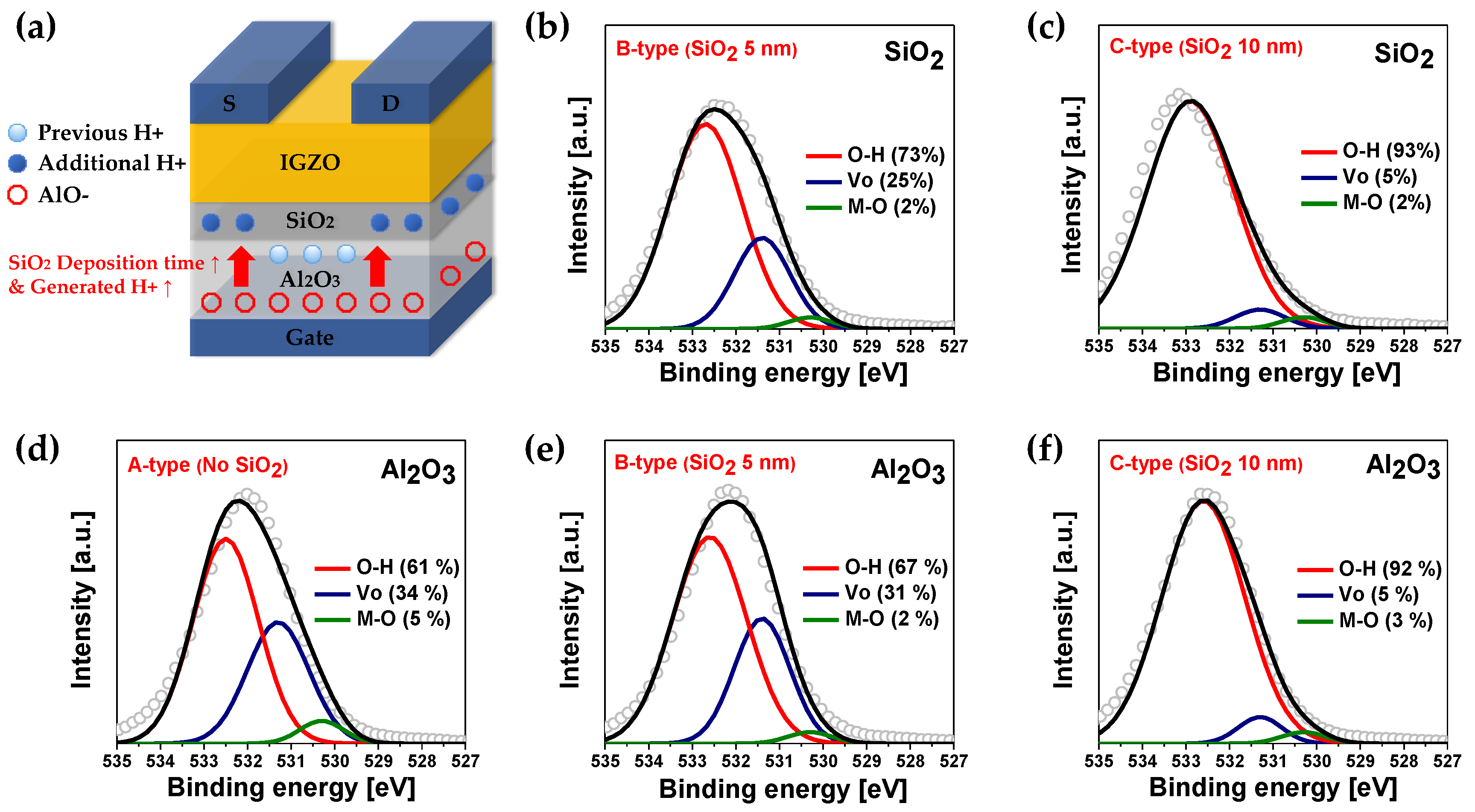
Figure 3a show the schematic view of hydrogen generation during the deposition of the SiO2 layer. When the LT ALD process is carried out for the Al2O3 deposition, residual hydrogen H is generated inside the Al2O3 layer due to incomplete chemical reaction between Al(CH3)3 and H2O [40,41]. Next, while the SiO2 layer is deposited on the Al2O3 layer, additional hydrogen is injected from the Al2O3 to the SiO2 layer. Figure 3b,c shows the XPS analysis of O 1 s in the SiO2 layer for the B- and C- type devices, respectively. The amount of hydrogen is verified through the O 1 s XPS spectrum, which is deconvoluted to three peaks of O-H, Vo, and M-O to analyze hydroxide, oxygen vacancy, and metal-oxygen content, respectively [42,43]. Hydrogen content in the SiO2 layer can be confirmed in the form of hydroxide, and it can be also observed that the C-type device with a thicker SiO2 has 20% more hydrogen than the B-type device. This is because a thicker SiO2 layer means a longer deposition time, and the existing Al-H bonds are more dissociated and injected into the SiO2 layer. The change of hydrogen content according to the SiO2 thickness shows a clear difference in the Al2O3 layer as shown in Figure 3d–f. The difference in hydrogen content between A-type and B-type is only 6%, while the difference between the A-type and C-type is 31%. This means that the B-type with 5-nm-thick SiO2 layer cannot generate significant hydrogen content compared to the C-type with SiO2 10 nm layer, and the C-type can be more suitable for memory device considering the VT modulation.

Figure 3.
Illustration of hydrogen movement in the Al2O3, SiO2 layer during the gate insulator deposition. (a) Schematic view of the IGZO synaptic TFTs with hydrogen movement by deposition process. O 1 s XPS spectra of Al2O3 layer in (b) B-type and (c) C-type IGZO synaptic TFTs in the SiO2 layer. O 1 s XPS spectra of Al2O3 layer in (d) A-type, (e) B-type, and (f) C-type IGZO synaptic TFTs in Al2O3 layer.
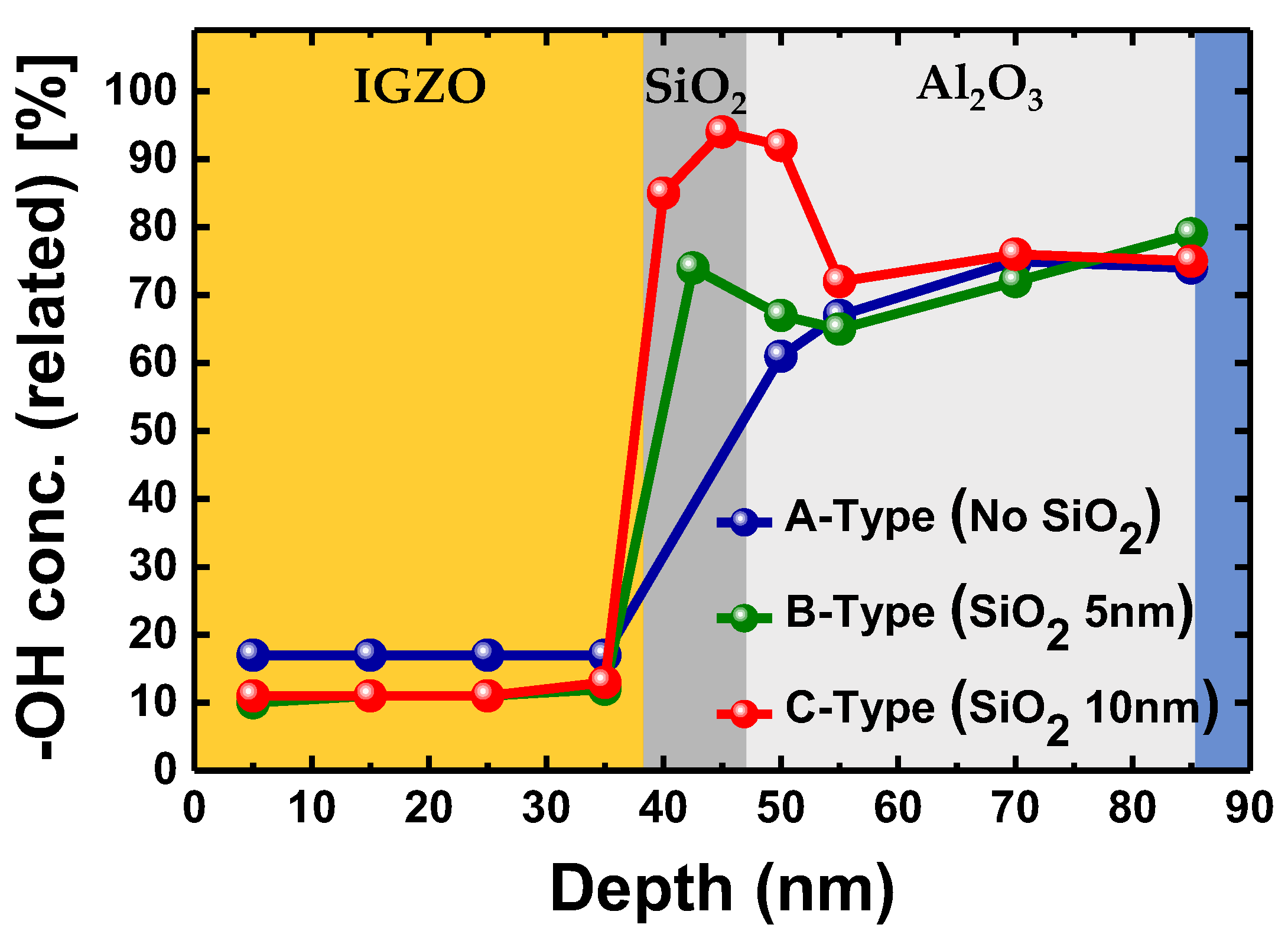
Moreover, we performed the additional XPS depth profile analysis of the entire stack for the IGZO TFTs to analyze the movement of hydrogen in detail during the gate insulator deposition step. Figure 4 summarizes the proportion of hydroxide in the total XPS depth profile analysis for the A-, B- and C-type devices. First, the hydrogen content in the IGZO channel of all the devices is lower than that of either the SiO2 or Al2O3 layer for the entire depth region. This is because the bond dissociation energy of Si-H (318 kJ/mol) and Al-H (285 kJ/mol) is higher than In-H (243 kJ/mol), Ga-H (274 kJ/mol), and Zn-H (85 kJ/mol), so the additionally generated hydrogen in the Al2O3 layer during the deposition process is hard to move toward the IGZO channel [44,45]. In addition, since hydrogen combines with oxygen to form an O-H bond when hydrogen reaches the IGZO interface, a large amount of hydrogen cannot move into the IGZO channels. Inside the SiO2 layer, the hydrogen content of the C-type device is much higher than that of the B-type device in all the regions. This is because the hydrogen content increases with the increased SiO2 deposition thickness because the existing Al-H bond is broken and injected into the SiO2 layer during the deposition step as discussed in Figure 3b,c. At 5 nm depth of the Al2O3 layer, the hydrogen content of the C-type is much higher than that of the A- and B-type devices. However, as the depth increases, there is no significant difference in the hydrogen content depending on the device type. This is because additionally generated hydrogen during the SiO2 deposition step moved into the SiO2 rather than the Al2O3 layer due to the difference in bond dissociation energy between Si-H and Al-H.
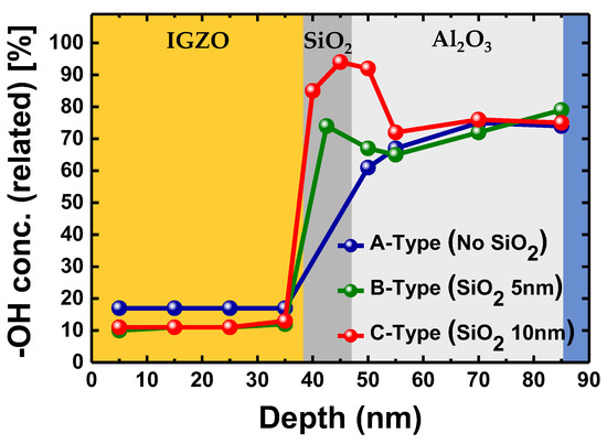
Figure 4.
XPS depth profile analysis of A-, B- and C-type IGZO TFTs. XPS analysis was performed at 5 nm, 15 nm, 25 nm, 35 nm depth in IGZO layer (all the types), 5 nm, 10 nm depth in SiO2 layer (B- and C-type only), and 5 nm, 10 nm, 25 nm, 40 nm depth in Al2O3 layer (all the types).
The stress-induced instability in the A- and C-type IGZO TFTs is also investigated by applying NBS and PBS at VGS = −15 V, and 10 V, respectively, for 1.8 ks as shown in Figure 5a,b. The C-type device is considered as potential candidate for synaptic device thanks to high hydrogen content and the A-type device is verified as reference device. The A-type IGZO TFT shows 3.6 V negative VT shift under PBS and 2 V positive VT shift under NBS, which means that hydrogen ions inside the Al2O3 and SiO2 layer move toward the IGZO channel during PBS but move away from the IGZO channel again during NBS due to negative VGS. Since the C-type IGZO TFT has more hydrogen content than the A-type device due to the additional SiO2 layer, it shows a larger VT shift under the same stress conditions (ΔVT = −7.9 V/6 V under PBS/NBS). The VT is recovered through NBS in both the A- and C-type devices, but not fully as the initial values since some of hydrogen moving toward the IGZO layer can form a bond with oxygen at the IGZO layer interface [40], and some hydrogen can act as a shallow donor [46]. Therefore, strong NBS condition with larger amplitude than PBS condition is required for sufficient VT recovery.
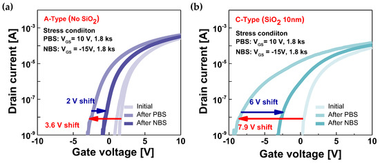
Figure 5.
I-V characteristics of with PBS (VGS = 10 V, 1.8 ks) and NBS (VGS = −15 V, 1.8 ks) for (a) A-type and (b) C-type.
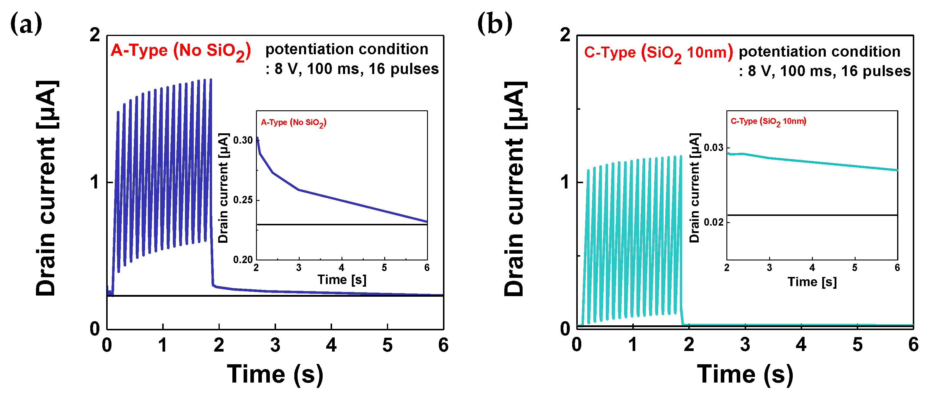
Figure 6a,b shows the retention characteristics after applying 16 potentiation pulses of VGS = 8 V with a width of 100 ms to the A- and C-type IGZO TFTs, respectively. After all the potentiation pulses are applied, both the drain current of both devices is slowly recovered to the initial state, indicating that hydrogen move inside the Al2O3 and SiO2 layer. However, the drain current of the A-type decreases rapidly, while that of the C-type remains higher than the initial value for 4 s after applying 16 potentiation pulses. The drain current of the A-type device decreased to almost the initial state (96% drop) for 4 s, but the C-type device maintained the drain current (27% drop) for 4 s. This is because the migration velocity of hydrogen in SiO2 is slower than that in Al2O3 [47], which implies that the insertion of the SiO2 layer improves not only the VT modulation window but also the retention characteristics.
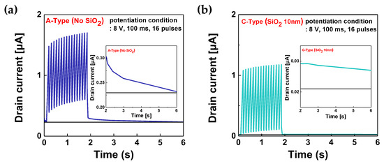
Figure 6.
Retention characteristics of (a) A-type and (b) C-type devices after 16 potentiation pulses with VGS = 8 V and 100 ms width.
4. Conclusions
In this study, we reported the effects of additional deposition of SiO2 on the Al2O3 layer as a gate insulator of the IGZO TFTs. A total of three types of the devices were fabricated with different gate insulator stacks and their electrical characteristics were compared to investigate the effect of the additional SiO2 layer. It was confirmed through the XPS analysis that hydrogen ions were additionally generated by inserting the SiO2 layer between the Al2O3 and IGZO layers. With increasing the SiO2 layer thickness, the VT memory window was improved under PBS and NBS conditions thanks to the increased hydrogen content. In addition, the retention properties were significantly improved as the migration velocity of hydrogen in SiO2 decreased. These results are expected to contribute to the optimization of the synaptic IGZO TFTs with LT processed gate insulators.
Author Contributions
Methodology, S.P. and J.T.J.; formal analysis, S.P. and S.Y.; writing—original draft preparation, S.Y.; writing—review and editing, H.K. and D.H.K.; project administration, H.K. and D.H.K.; funding acquisition, H.K. and D.H.K. S.P. and S.Y. equally contributed to this work. All authors have read and agreed to the published version of the manuscript.
Funding
This work was supported in part by the National Research Foundation of Korea (NRF) grant funded by the Korea Government (MSIT) (No. 2016R1A5A1012966, 25%, No. 2020R1A2B5B01001979, 25%, and No. 2020M3F3A2A01081656, 35%), partly by the Institute of Information and Communications Technology Planning and Evaluation (IITP) grant funded by the Korea government (MSIT) (No. 2021-0-01764, 15%), and in part by the Brain Korea 21 Four Program.
Institutional Review Board Statement
Not applicable.
Informed Consent Statement
Not applicable.
Data Availability Statement
The data presented in this study are available on request from the corresponding author.
Conflicts of Interest
The authors declare no conflict of interest.
References
- Backus, J. Can programming be liberated from the von Neumann style? A functional style and its algebra of programs. Commun. ACM 1978, 21, 613–641. [Google Scholar] [CrossRef] [Green Version]
- Mead, C. How we created neuromorphic engineering. Nat. Electron. 2020, 3, 434–435. [Google Scholar] [CrossRef]
- Nawrocki, R.A.; Voyles, R.M.; Shaheen, S.E. A mini review of neuromorphic architectures and implementations. IEEE Trans. Electron. Devices 2016, 63, 3819–3829. [Google Scholar] [CrossRef]
- Sharifshazileh, M.; Burelo, K.; Sarnthein, J.; Indiveri, G. An electronic neuromorphic system for real-time detection of high frequency oscillations (HFO) in intracranial EEG. Nat. Commun. 2021, 12, 3095. [Google Scholar] [CrossRef] [PubMed]
- Wang, Y.; Yin, L.; Huang, W.; Li, Y.; Huang, S.; Zhu, Y.; Yang, D.; Pi, X. Optoelectronic synaptic devices for neuromorphic computing. Adv. Intell. Syst. 2021, 3, 2000099. [Google Scholar] [CrossRef]
- Morozov, A.Y.; Abgaryan, K.K.; Reviznikov, D.L. Mathematical model of a neuromorphic network based on memristive elements. Chaos Solit. Fractals 2021, 143, 110548. [Google Scholar] [CrossRef]
- Feng, Y.; Huang, P.; Zhao, Y.; Shan, Y.; Zhang, Y.; Zhou, Z.; Liu, L.; Liu, X.; Kang, J. Improvement of state stability in multi-level resistive random-access memory (RRAM) array for neuromorphic computing. IEEE Electron. Device Lett. 2021, 42, 1168–1171. [Google Scholar] [CrossRef]
- Prezioso, M.; Mahmoodi, M.; Bayat, F.M.; Nili, H.; Kim, H.; Vincent, A.; Strukov, D. Spike-timing-dependent plasticity learning of coincidence detection with passively integrated memristive circuits. Nat. Commun. 2018, 9, 5311. [Google Scholar] [CrossRef] [Green Version]
- Ambrogio, S.; Ciocchini, N.; Laudato, M.; Milo, V.; Pirovano, A.; Fantini, P.; Ielmini, D. Unsupervised learning by spike timing dependent plasticity in phase change memory (PCM) synapses. Front. Neurosci. 2016, 10, 56. [Google Scholar] [CrossRef] [Green Version]
- Kim, H.; Mahmoodi, M.; Nili, H.; Strukov, D.B. 4K-memristor analog-grade passive crossbar circuit. Nat. Commun. 2021, 12, 5198. [Google Scholar] [CrossRef]
- Li, Y.; Ang, K.-W. Hardware implementation of neuromorphic computing using large-scale memristor crossbar arrays. Adv. Intell. Syst. 2021, 3, 2000137. [Google Scholar] [CrossRef]
- Kim, T.-H.; Lee, J.; Kim, S.; Park, J.; Park, B.-G.; Kim, H. 3-bit multilevel operation with accurate programming scheme in TiOx/Al2O3 memristor crossbar array for quantized neuromorphic system. Nanotechnology 2021, 32, 295201. [Google Scholar] [CrossRef] [PubMed]
- Jeon, K.; Kim, J.; Ryu, J.J.; Yoo, S.-J.; Song, C.; Yang, M.K.; Jeong, D.S.; Kim, G.H. Self-rectifying resistive memory in passive crossbar arrays. Nat. Commun. 2021, 12, 1–15. [Google Scholar] [CrossRef] [PubMed]
- Kim, T.-H.; Kim, S.; Hong, K.; Park, J.; Hwang, Y.; Park, B.-G.; Kim, H. Multilevel switching memristor by compliance current adjustment for off-chip training of neuromorphic system. Chaos Solit. Fractals 2021, 153, 111587. [Google Scholar] [CrossRef]
- Hsieh, E.; Zheng, X.; Le, B.; Shih, Y.; Radway, R.; Nelson, M.; Mitra, S.; Wong, S. Four-bits-per-memory one-transistor-and-eight-resistive-random-access-memory (1T8R) array. IEEE Electron. Device Lett. 2021, 42, 335–338. [Google Scholar] [CrossRef]
- Jang, J.T.; Min, J.; Hwang, Y.; Choi, S.-J.; Kim, D.M.; Kim, H.; Kim, D.H. Digital and analog switching characteristics of InGaZnO memristor depending on top electrode material for neuromorphic system. IEEE Access 2020, 8, 192304–192311. [Google Scholar] [CrossRef]
- Joshi, V.; Le Gallo, M.; Haefeli, S.; Boybat, I.; Nandakumar, S.R.; Piveteau, C.; Dazzi, M.; Rajendran, B.; Sebastian, A.; Eleftheriou, E. Accurate deep neural network inference using computational phase-change memory. Nat. Commun. 2020, 11, 2473. [Google Scholar] [CrossRef]
- Yin, Q.; Chen, L. Crystallization behavior and electrical characteristics of Ga–Sb thin films for phase change memory. Nanotechnology 2020, 31, 215709. [Google Scholar] [CrossRef]
- Kim, T.; Lee, S. Evolution of phase-change memory for the storage-class memory and beyond. IEEE Trans. Electron. Devices 2020, 67, 1394–1406. [Google Scholar] [CrossRef]
- Li, C.; An, J.; Kweon, J.Y.; Song, Y.-H. Alternate pulse scheme in a hardware neural network for reducing the influence of asymmetry on synaptic weight updating. J. Semicond. Technol. Sci. 2020, 20, 119–126. [Google Scholar] [CrossRef]
- Kim, H.; Park, J.; Kwon, M.-W.; Lee, J.-H.; Park, B.-G. Silicon-based floating-body synaptic transistor with frequency-dependent short-and long-term memories. IEEE Electron. Device Lett. 2016, 37, 249–252. [Google Scholar] [CrossRef]
- Mulaosmanovic, H.; Ocker, J.; Müller, S.; Noack, M.; Müller, J.; Polakowski, P.; Mikolajick, T.; Slesazeck, S. Novel ferroelectric FET based synapse for neuromorphic systems. In Proceedings of the 2017 Symposium on VLSI Technology, Kyoto, Japan, 5–8 June 2017; pp. T176–T177. [Google Scholar]
- Nguyen, M.-C.; Lee, K.; Kim, S.; Youn, S.; Hwang, Y.; Kim, H.; Choi, R.; Kwon, D. Incremental drain-voltage-ramping training method for ferroelectric field-effect transistor synaptic devices. IEEE Electron. Device Lett. 2022, 43, 17–20. [Google Scholar] [CrossRef]
- Kim, S.K.; Geum, D.-M.; Lim, H.-R.; Han, J.; Kim, H.; Jeong, Y.; Kim, S.-H. Photo-responsible synapse using Ge synaptic transistors and GaAs photodetectors. IEEE Electron. Device Lett. 2020, 41, 605–608. [Google Scholar] [CrossRef]
- Lee, C.; Choi, W.; Kwak, M.; Kim, S.; Hwang, H. Impact of electrolyte density on synaptic characteristics of oxygen-based ionic synaptic transistor. Appl. Phys. Lett. 2021, 119, 103503. [Google Scholar] [CrossRef]
- Choi, H.-S.; Kim, H.; Lee, J.-H.; Park, B.-G.; Kim, Y. AND flash array based on charge trap flash for implementation of convolutional neural networks. IEEE Electron. Device Lett. 2020, 41, 1653–1656. [Google Scholar] [CrossRef]
- Lan, S.; Ke, Y.; Chen, H. Photonic synaptic transistor based on p-type organic semiconductor blending with n-type organic semiconductor. IEEE Electron. Device Lett. 2021, 42, 1180–1183. [Google Scholar] [CrossRef]
- Hwang, S.; Yu, J.; Lee, G.H.; Song, M.S.; Chang, J.; Min, K.K.; Jang, T.; Lee, J.-H.; Park, B.-G.; Kim, H. Capacitor-based synaptic devices for hardware spiking neural networks. IEEE Electron. Device Lett. 2022, 43, 549–552. [Google Scholar] [CrossRef]
- Kim, S.; Baek, M.-H.; Hwang, S.; Jang, T.; Park, K.; Park, B.-G. A novel vector-matrix multiplication (VMM) architecture based on NAND memory array. J. Semicond. Technol. Sci. 2020, 20, 242–248. [Google Scholar] [CrossRef]
- Li, L.; Shao, Y.; Wang, X.; Wu, X.; Liu, W.-J.; Zhang, D.W.; Ding, S.-J. Flexible femtojoule energy-consumption In-Ga-Zn-O synaptic transistors with extensively tunable memory time. IEEE Trans. Electron. Devices 2019, 67, 105–112. [Google Scholar] [CrossRef]
- Yang, Y.; He, Y.; Nie, S.; Shi, Y.; Wan, Q. Light stimulated IGZO-based electric-double-layer transistors for photoelectric neuromorphic devices. IEEE Electron. Device Lett. 2018, 39, 897–900. [Google Scholar] [CrossRef]
- Kim, J.; Kim, Y.; Kwon, O.; Kim, T.; Oh, S.; Jin, S.; Park, W.; Kwon, J.D.; Hong, S.W.; Lee, C.S. Modulation of synaptic plasticity mimicked in al nanoparticle-embedded IGZO synaptic transistor. Adv. Electron. Mater. 2020, 6, 1901072. [Google Scholar] [CrossRef]
- Zhu, L.; He, Y.; Chen, C.; Zhu, Y.; Shi, Y.; Wan, Q. Synergistic modulation of synaptic plasticity in IGZO-based photoelectric neuromorphic TFTs. IEEE Trans. Electron. Devices 2021, 68, 1659–1663. [Google Scholar] [CrossRef]
- Li, S.; Lyu, H.; Li, J.; He, Y.; Gao, X.; Wan, Q.; Shi, Y.; Pan, L. Multiterminal ionic synaptic transistor with artificial blink reflex function. IEEE Electron. Device Lett. 2021, 42, 351–354. [Google Scholar] [CrossRef]
- Park, S.; Jang, J.T.; Choi, S.-J.; Kim, D.M.; Kim, D.H. Synaptic behavior of flexible IGZO TFTs with Al2O3 gate insulator by low temperature ALD. In Proceedings of the 2019 IEEE 19th International Conference on Nanotechnology (IEEE-NANO), Macao, China, 22–26 July 2019; pp. 517–520. [Google Scholar]
- Kim, J.-H.; Seo, Y.; Jang, J.T.; Park, S.; Kang, D.; Park, J.; Han, M.; Kim, C.; Park, D.-W.; Kim, D.H. Reliability-aware SPICE compatible compact modeling of IGZO inverters on a flexible substrate. Appl. Sci. 2021, 11, 4838. [Google Scholar] [CrossRef]
- Park, S.; Jang, J.T.; Hwang, Y.; Lee, H.; Choi, W.S.; Kang, D.; Kim, C.; Kim, H.; Kim, D.H. Effect of the gate dielectric layer of flexible InGaZnO synaptic thin-film transistors on learning behavior. ACS App. Electron. Mater. 2021, 3, 3972–3979. [Google Scholar] [CrossRef]
- Oh, S.-I.; Woo, J.-M.; Jang, J.-H. Comparative studies of long-term ambiance and electrical stress stability of IGZO thin-film transistors annealed under hydrogen and nitrogen ambiance. IEEE Trans. Electron. Devices 2016, 63, 1910–1915. [Google Scholar] [CrossRef]
- Kang, Y.; Ahn, B.D.; Song, J.H.; Mo, Y.G.; Nahm, H.H.; Han, S.; Jeong, J.K. Hydrogen bistability as the origin of photo-bias-thermal instabilities in amorphous oxide semiconductors. Adv. Electron. Mater. 2015, 1, 1400006. [Google Scholar] [CrossRef]
- Chang, Y.-H.; Yu, M.-J.; Lin, R.-P.; Hsu, C.-P.; Hou, T.-H. Abnormal positive bias stress instability of In–Ga–Zn–O thin-film transistors with low-temperature Al2O3 gate dielectric. Appl. Phys. Lett. 2016, 108, 033502. [Google Scholar] [CrossRef] [Green Version]
- Guerra-Nuñez, C.; Döbeli, M.; Michler, J.; Utke, I. Reaction and growth mechanisms in Al2O3 deposited via atomic layer deposition: Elucidating the hydrogen source. Chem. Mater. 2017, 29, 8690–8703. [Google Scholar] [CrossRef]
- Xia, G.; Zhang, Q.; Wang, S. High-mobility IGZO TFTs by infrared radiation activated low-temperature solution process. IEEE Electron. Device Lett. 2018, 39, 1868–1871. [Google Scholar] [CrossRef]
- Um, J.K.; Lee, S.; Jin, S.; Mativenga, M.; Oh, S.Y.; Lee, C.H.; Jang, J. High-performance homojunction a-IGZO TFTs with selectively defined low-resistive a-IGZO source/drain electrodes. IEEE Trans. Electron. Devices 2015, 62, 2212–2218. [Google Scholar]
- Cottrell, T.L. The Strengths of Chemical Bonds; Butterworths Scientific Publications: London, UK, 1958. [Google Scholar]
- Luo, Y.-R.; Kerr, J.A. Bond dissociation energies. In CRC Handbook of Chemistry and Physics; CRC Press/Taylor and Francis: Boca Ranton, FL, USA, 2012; Volume 89, p. 89. [Google Scholar]
- Chen, C.; Cheng, K.C.; Chagarov, E.; Kanicki, J. Crystalline In–Ga–Zn–O density of states and energy band structure calculation using density function theory. Jpn. J. Appl. Phys. 2011, 50, 091102. [Google Scholar] [CrossRef]
- Martin, D.; Duprez, D. Mobility of surface species on oxides. 2. Isotopic exchange of D2 with H of SiO2, Al2O3, ZrO2, MgO, and CeO2: Activation by rhodium and effect of chlorine. J. Phys. Chem. B 1997, 101, 4428–4436. [Google Scholar] [CrossRef]

Publisher’s Note: MDPI stays neutral with regard to jurisdictional claims in published maps and institutional affiliations. |
© 2022 by the authors. Licensee MDPI, Basel, Switzerland. This article is an open access article distributed under the terms and conditions of the Creative Commons Attribution (CC BY) license (https://creativecommons.org/licenses/by/4.0/).