Abstract
The monoclinic and hexagonal gallium tellurides (m-GaTe and h-GaTe) show different applications in optoelectronic devices. Compared to the m-GaTe, the h-GaTe is a metastable phase, which generally exists in ultrathin samples and is difficult to obtain by direct chemical reaction. Herein, a hexagonal ZnO-induced crystal growth strategy was used for the design and fabrication of h-GaTe. The high-quality h-GaTe nanosheets were successfully grown on the (001) surface of hexagonal ZnO by the chemical vapor deposition method under ambient pressure. The SEM, XPS, XRD, and HRTEM characterizations uncovered a flower-like nanosheet morphology and a hexagonal crystal structure for the obtained GaTe samples. Meanwhile, the conductive atomic force microscope measurement indicates that the obtained h-GaTe nanosheet is a p-type semiconductor. Based on the electron localization function simulation, the lattice-induced crystal growth of h-GaTe was demonstrated. The results give an insight into the synthesis of metastable phase crystal and open an avenue for fabricating new two-dimensional devices by p-type h-GaTe.
1. Introduction
Recently, two-dimensional (2D) materials have received increased attentions because of their potential applications in next-generation electronic and optoelectronic devices [1,2,3,4,5,6]. As a typical p-type material, GaTe has been widely used in random lasers and photodetectors, and for water splitting [7,8,9,10,11]. Meanwhile, to achieve the applications, all kinds of GaTe nanostructures, including 1D nanowires, 2D nanoflakes, and thin film, have been fabricated by physical vapor deposition (PVD), chemical vapor deposition (CVD), or molecular beam epitaxy (MBE) [12,13,14,15,16]. However, most of the fabricated GaTe samples crystallize in a monoclinic system with low symmetry space group. Compared to the m-GaTe, h-GaTe is a metastable phase, which generally exists in ultrathin samples. To obtain h-GaTe, over the previous decades, a lattice-induced strategy has been tried on Si (111), GaAs (111), c-sapphire, or mica substrates. Among them, h-GaTe can be grown on c-sapphire or mica substrates in a narrow temperature growth region and shows a low yield [17,18,19]. What is more, the reproducibility for the growth of h-GaTe in these experiments is still a big challenge. Hence, a reliable and highly efficient synthesis method for the h-GaTe is still expected.
In this work, the h-GaTe 2D nanosheets were successfully fabricated by a hexagonal ZnO-induced crystal growth strategy. Utilizing hexagonal ZnO nanocrystals as the substrate, the high-quality h-GaTe was grown by the simple CVD method under ambient pressure. It is worth noting that the synthesis has a high yield, and the hexagonal ZnO-induced h-GaTe growth shows a high reproducibility. Scanning electron microscope (SEM) and transmission electron microscope (TEM) images indicate that the formed flower-like h-GaTe nanosheets are assembled by 2D GaTe triangles. X-ray photoelectron spectroscopy (XPS), X-ray diffraction (XRD), and high-resolution TEM (HRTEM) uncover the hexagonal crystal structure in the obtained GaTe nanosheets. Meanwhile, the electron localization function simulation confirms the lattice-induced crystal growth mechanism for the growth of h-GaTe on hexagonal ZnO. The h-GaTe nanosheets show a p-type characteristic. In addition, the electronic structure of h-GaTe and the interfacial properties of GaTe/ZnO heterostructure were also investigated by first-principle calculations.
2. Experimental Section
2.1. Growth of ZnO Nanocrystals
Zinc powder (~50 mg, 99.99%, from Sigma-Aldrich, Burlington, MA, USA) in an alumina boat was placed at the upstream in a furnace (1 in.) and was used as the growth source of ZnO nanocrystals. A 10 × 10 mm n-type Si (resistivity: 0.001–0.005 Ω·cm, <100>) was adopted as the support and placed downstream ~3 cm away from the Zn source in the furnace. The source temperature was then heated to 800 °C from room temperature in 30 min and held for 10 min. During the growth, 100 standard state cubic centimeter per minute (sccm) Ar gas and 50 sccm mix gas of Ar and O2 (1% O2, 99% Ar) were used as transport gas to carry the zinc and oxygen to the growth substrate for reaction. Subsequently, the furnace was cooled down naturally to room temperature. The resultant ZnO nanocrystals were harvested on the surface of the Si support.
2.2. Growth of GaTe
The synthesis of h-GaTe was carried out in a tube furnace system with quartz reaction tube of 1 in. The as-grown ZnO/Si substrate was put upside-down on an aluminum boat with ~100 mg GaTe (99.99%, from Sigma-Aldrich, Burlington, MA, USA) power inside. The furnace was evacuated to 1 mbar and was purged with Ar (500 sccm) for 2 h to remove the oxygen residue. Then, the furnace temperature was increased to 750 °C at a rate of 20 °C min−1 under 100 sccm Ar gas. The growth of h-GaTe took place at ambient pressure. After reaction for 30 min, the furnace was cooled down to room temperature under Ar gas flow.
2.3. Material Characterization
The morphology and atomic structure of samples were investigated by SEM (Hitachi S4800, Japan) and scanning transmission electron microscopy (STEM) (JEOL 2100, Tokyo, Japan). The samples were also measured using AFM (Dimension Fastscan, Bruker, Karlsruhe, Germany) operated in peak-force trapping mode. XPS (ESCALAB 250Xi, Thermo Fisher Scientific, Waltham, MA, USA) was used to conduct chemical component analysis. Raman and PL spectra were performed on a commercial system (Witec Ulm Germany/Izasa, Carnaxide, Portugal) using a 532-nm laser for excitation. The laser power was kept at 0.5–1 mW. XRD analysis (PANalytical, operating at 40 kV and 40 mA, with Cu radiation ( = 0.1541874 nm) was performed to identify the crystallinity of the samples.
2.4. DFT for the Atomic and Electronic Structures
Density functional theory calculations were performed by the Vienna Ab initio Simulation Package (VASP) [20]. The projector-augmented wave (PAW) was employed for the electron-ion interaction [21], and plane-wave basis was set with an energy cutoff of 260 eV. Van der Waals (vdWs) interaction was taken into account with the optB86b vdW exchange-correlation function [22]. The maximum residual force during geometry optimization was below 0.01 eV/Å, and energies were converged to less than 1 × 10⁻³ eV per atom. The Monkhorst-Pack k-point mesh was sampled with a separation of about 0.01 Å−1 in the Brillouin zone. A supercell of the ZnO/GaTe heterostructure with the lattice parameter a = b = 8.27 Å was built. The interlayer distance between h-GaTe and ZnO was 2.66 Å, and the lattice mismatch was within 1%.
3. Results and Discussion
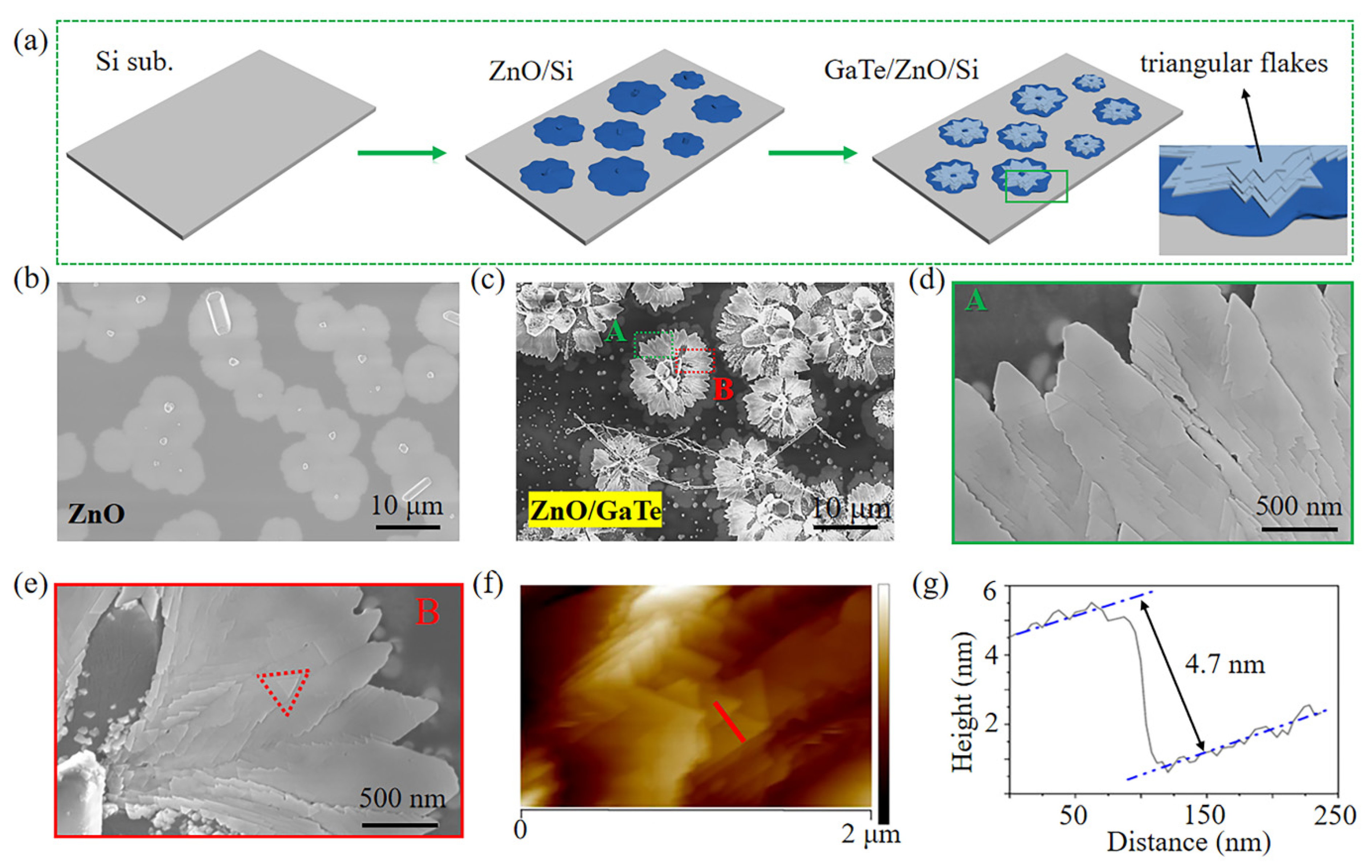
Figure 1a outlines the two-step procedure adopted to grow the flower-like GaTe nanosheets. The ZnO nanocrystals were grown on the Si wafer via the first growth step (Figure 1b), and GaTe flower-like nanosheets were synthesized on the ZnO/Si wafer via the second growth step (Figure 1c). Details of the growth process can be found in the Experimental Section. The ZnO nanocrystals with hexagonal symmetry as the buffer layer promoted the growth of h-GaTe (with triangular morphology). Furthermore, the high-magnification SEM images (Figure 1d,e) clearly reveal that the grown GaTe nanosheets are well aligned and integrated with ZnO nanocrystals. The GaTe nanosheets are distributed horizontally on the ZnO surface, forming a flower-like morphology. The GaTe nanosheets prefer to grow around the (001) basal plane of ZnO due to its lower surface energy [23]. Further energy dispersive spectroscopy (SEM-EDS) for the ZnO nanocrystals and GaTe nanosheets reveals Zn, O, Ga, and Te signals, confirming their elemental composition (Figure S1, see Supplementary Materials). Figure 1f shows an atomic force microscopy (AFM) image of the GaTe nanosheets, which exhibits a clearly-layered structure with a multi-layered feature, implying that the flower consists of GaTe nanosheets with different layer numbers. As shown in Figure 1g, the thickness of the GaTe triangle is ~4.7 nm, which corresponds to six layers because one single-layer GaTe has a thickness of ~0.8 nm [16].

Figure 1.
(a) Fabrication process of GaTe nanosheet flower by a two-step CVD process. (b) SEM image of ZnO islands obtained using the CVD method. (c) SEM image of GaTe nanosheet flower. (d,e) High-magnification SEM images of the regions marked by a green (A) and a red (B) rectangle in (c), showing that the petals are formed from GaTe triangular flakes. (f) AFM image of the petals of GaTe nanosheet flower. (g) Height profile along the line marked in (f), revealing that the thickness of GaTe triangles is ~4.7 nm.
XPS analysis was performed to investigate the chemical composition, as shown in Figure 2a, presenting the XPS spectrum of the GaTe nanosheets. Ga and Te elements are from GaTe grown in the second growth step and Zn and O from the ZnO nanocrystals serving as nucleation sites in the first step. In the XPS spectrum of Zn (Figure 2b), there emerge strong peaks at 1045.4 and 1022 eV, which correspond to Zn 2p1/2 and Zn 2p3/2 in ZnO, respectively. The Zn peaks are attributed to the ZnO molecular environment [24]. The Ga 3d peak in Figure 2c is located at 20.2, while a shoulder at 22.6 eV is observed and has been explained by an emission of the oxygen 2s level [9]. In addition, as shown in Figure 2d, there are two distinct Te 3d3/2 and 3d5/2 peaks at 582.5 and 572.2 eV, which correspond to those of GaTe [25]. The appearance of peaks at 586.7 and 576.6 eV indicates the presence of TeO2, mainly due to the oxidation of Te [26].
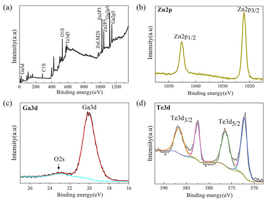
Figure 2.
High resolution XPS spectra of the GaTe nanosheet flower. (a) XPS spectrum. Four elements are present in the spectrum: Ga and Te, from the second-step CVD products, and Zn and O, from the ZnO nanocrystals. The core levels of (b) Zn (2p1/2 and 2p3/2), (c) Ga (3d), and (d) Te (3d3/2 and 3d5/2).
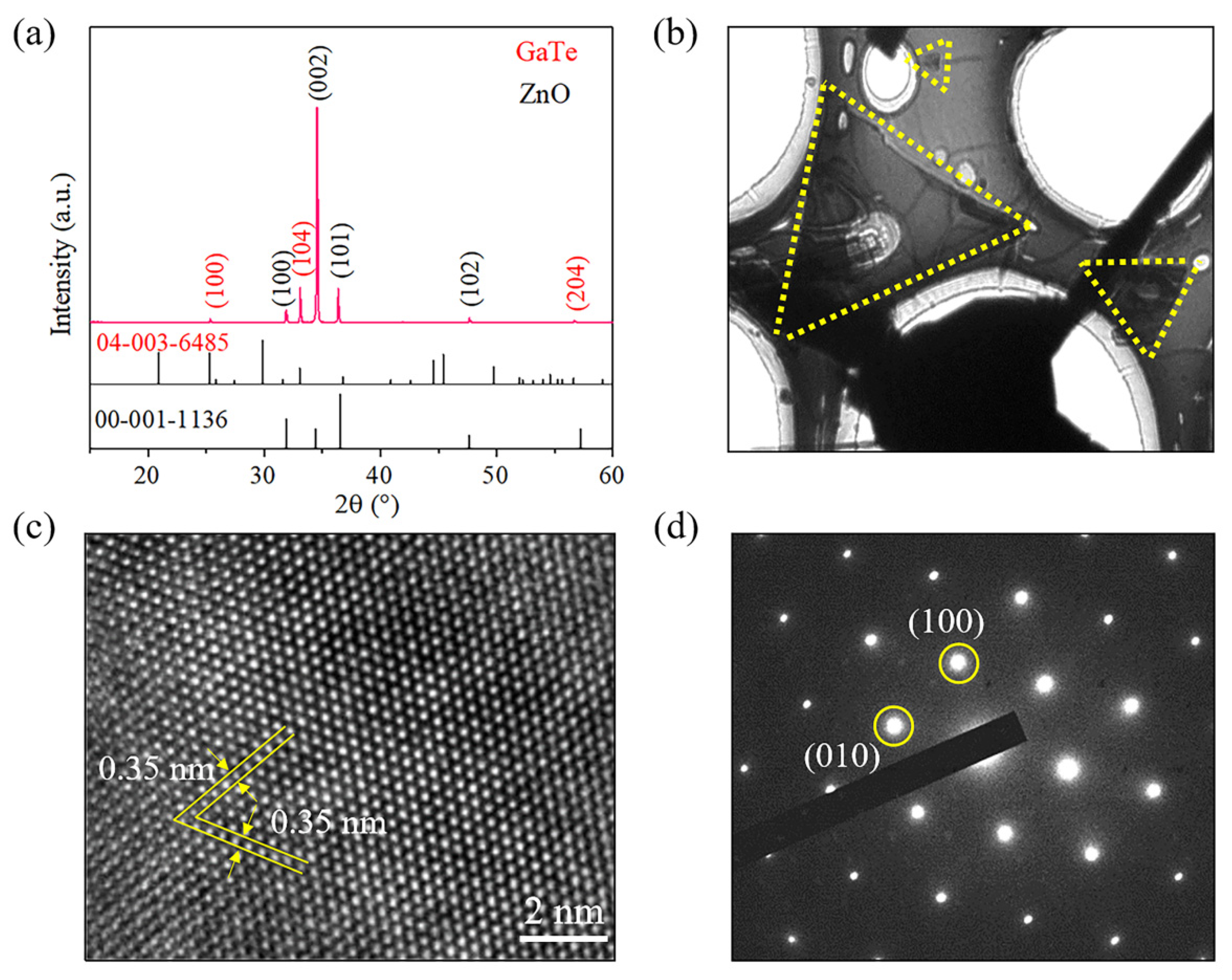
To investigate the crystallinity of the as-prepared samples, XRD analysis of the GaTe nanosheets is shown in Figure 3a. The diffraction peaks at 2θ = 31.8°, 34.3°, 36.5°, and 57.2° correspond to the (100), (002), (101), and (102) planes of the ZnO hexagonal phase (JCPDS 00-001-1136, a = 0.324 nm and c = 0.517 nm), respectively [27,28]. In addition, there emerge diffraction peaks at 2θ = 25.3°, 33.1°, and 56.6°, which can be attributed to the (100), (104), and (204) planes of GaTe, respectively. The XRD pattern is well consistent with that of h-GaTe (JCPDS no. 04-003-6485 (P63/mmc)), confirming that the as-synthesized nanosheets have a h-GaTe phase [29]. To further conduct TEM observation to probe the crystallinity of the GaTe nanosheets, the ultrasonic-treated nanosheet sample was transferred onto a quantifoil copper TEM grid [30,31], as shown in Figure 3b. Figure 3c shows a high-resolution TEM (HRTEM) image of a circle area in Figure 3b, in which a hexagonal arrangement can be clearly observed. A further selected area electron diffraction (SAED) pattern (Figure 3d) of the 2D GaTe triangle exhibits a pattern with six-fold symmetry diffraction spots, confirming the single-crystalline nature of GaTe nanosheets. The spot pattern can be well indexed to h-GaTe (JCPDS no. 01-089-2675 (P63/mmc)) with lattice parameters of a = 0.406 nm and c = 1.696 nm [32,33].
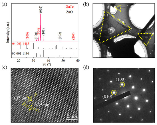
Figure 3.
(a) XRD pattern of the as-synthesized GaTe nanosheet flower. (b) Low-magnification high-angle annular dark-field (HAADF) image of GaTe nanosheet. (c) HRTEM image. (d) SAED pattern of the 2D GaTe nanosheet, revealing that the 2D GaTe nanosheet has a single-crystal wurtzite structure.
To examine the quality of the flower-like GaTe nanosheets, Raman spectrum and intensity mapping was conducted to investigate the lattice vibration of the GaTe nanosheets (Figure 4a) [34]. As shown in Figure 4b, six Raman peaks are identified approximately at 102, 126, 143, 330, 383, and 438 cm−1. The peaks at 126 and 143 cm−1 correspond to the Ag modes of GaTe [35,36,37]. The peak at ~102 cm−1 reflects the E2L line from the wurtzite ZnO nanocrystals, which is derived from the zone folding of the transverse acoustic (TA) mode in ZnO [38]. The peak at 383 cm−1 corresponds to A1T and that at 438 cm−1 to E2H of ZnO. The peak at ~330 cm−1 is attributed to the second-order Raman processes, which corresponds to E2H-2L of ZnO [39]. To investigate the spatial variation of the peak intensity, Raman intensity mapping of the flower-like GaTe nanosheets (see Figure 4a) was performed, as shown in Figure 4c, where one can notice the Raman intensity map of the Ag mode (~126 cm−1) of GaTe with an intensity distribution over the surface of the GaTe nanosheets. Obviously, the high intensity region (the bright spot at the center) corresponds to the area covered with GaTe nanosheets.

Figure 4.
Optical properties of the GaTe nanosheet flower. (a) SEM image of a flower-like GaTe nanosheet. The inset magnifies the region marked by a pink rectangle, which shows clearly that both the surface and the side of the ZnO nanorod are densely packed with GaTe nanosheets. (b) Raman spectrum for the GaTe nanosheet flower. (c) Raman mapping and the corresponding SEM image is shown in (a). The size of the area adopted for Raman mapping is 15 × 15 μm.
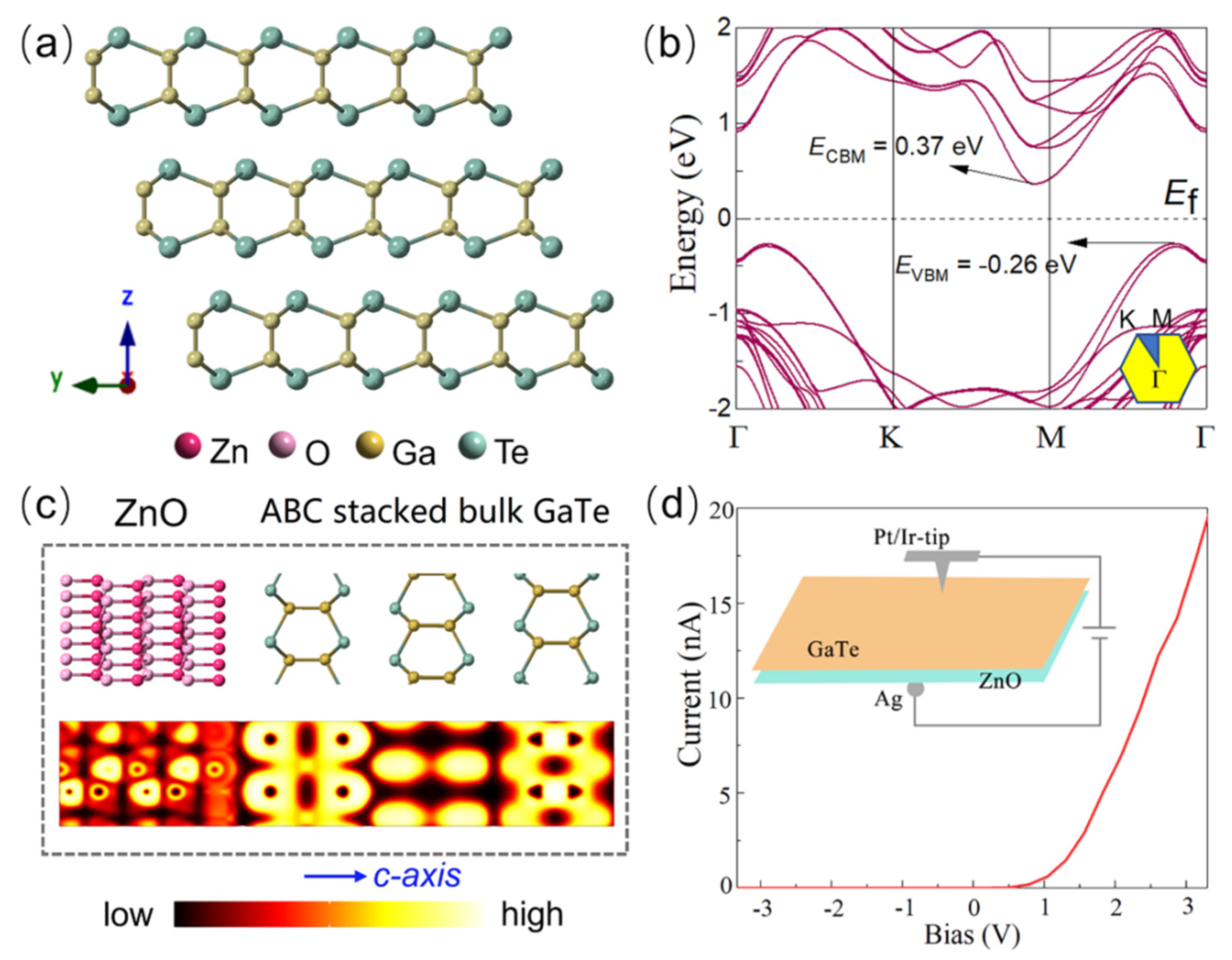
DFT is typically used to predict structures and calculate band information [40,41]. Figure 5a shows the side view of ABC-stacked h-GaTe, and the calculated band gap structure is shown in Figure 5b. The conduction-band minimum (CBM) is located at 0.37 eV, and the valence-band maximum (VBM) is located at 0.26 eV. Obviously, the results demonstrate that h-GaTe is a p-type semiconductor with an indirect bandgap. To further investigate the electron localization at the interface of the ZnO/GaTe heterostructure, an electron localization function simulation is employed. The heterostructure and calculated results are shown in Figure 5c, showing a stronger interaction in the interface of the ZnO/GaTe heterostructure compared to van der Waals force in the interlamination of pure GaTe. According to the DFT results, we attribute the structural transformation to the strongly interfacial interaction, together with the hexagonally symmetric ZnO seed layer.
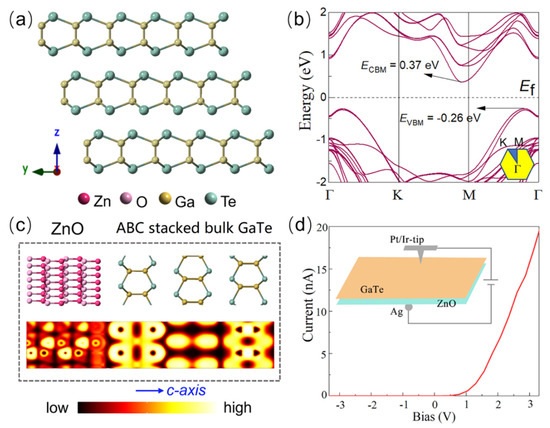
Figure 5.
(a) The side view of the ABC-stacked h−GaTe. (b) Band structure of the ABC−stacked bulk GaTe. Ef denote fermi level. (c) Electron localization function of the stacked heterostructure. (d) I-V curve of the p−GaTe/n−ZnO heterojunction. Inset: Diagram of the conductive atomic force microscope (CAFM) measurement. The contacts for the diode are realized by an Ag back electrode to the ZnO film and a local electrode (Pt/Ir−tip) to the intrinsically p−type GaTe nanosheet flower.
One of the most important advantages of GaTe over other 2D semiconductors is the p-type conductivity. Furthermore, ZnO is known as an intrinsic n-type semiconductor. Hence, p-type GaTe can naturally form heterostructure p-n junctions with n-type ZnO, which may enable many optoelectronics applications. Here we employed a conductive atomic force microscope (CAFM) technique to measure the vertical charge transport of GaTe/ZnO. The geometry of the experimental setup is shown in the inset of Figure 5d. A conductive Pt/Ir-coated Si tip served as positionable tip to the surface of the GaTe nanosheet flower, which forms an Ohmic contact to the GaTe nanosheet flower due to the package materials (Pt/Ir) with high work function and the tight contact force between the probe and sample under the CAFM mode [39]. Silver (Ag) paste is used as the second contact to the n-type ZnO film to obtain Ohmic contact, enabling the current through the p-GaTe/n-ZnO heterojunction diodes [42]. The CAFM measurements demonstrate that the as-grown sample has a slightly stronger rectifying feature, with typical I-V characteristics shown in Figure 5d.
4. Conclusions
In summary, a lattice-induced strategy was successfully applied for the growth of high-quality h-GaTe crystals by the CVD method under ambient pressure. The synthesis, showing a high yield and a high reproducibility, could be a promising route for the massive fabrication of high-quality h-GaTe. The morphology and crystal structure of the obtained h-GaTe were confirmed by SEM, TEM, XRD, Raman, and XPS spectra. Meanwhile, the CAFM measurements demonstrate that the h-GaTe/ZnO heterostructure has a rectifying feature, which is suitable for the application of photodiode. Moreover, the self-organized growth of 2D GaTe nanosheets on ZnO nanocrystals is stable in air or water and can be used as a catalyst for heterojunctional water splitting.
Supplementary Materials
The following supporting information can be downloaded at: https://www.mdpi.com/article/10.3390/cryst12050627/s1. See the Figure S1 for the EDS of ZnO and ZnO/GaTe, and the Figure S2 for the m−GaTe synthesizing on Si wafer.
Author Contributions
Conceptualization, Z.C.; methodology, Q.C.; formal analysis, Y.C.; writing—original draft preparation, Q.C.; writing—review and editing, J.W. and Z.C.; supervision, M.L. and Z.C.; project administration, Z.C.; All authors have read and agreed to the published version of the manuscript.
Funding
This research was funded by the National Natural Science Foundation of China (Grant No. 62104073) and the China Postdoctoral Science Foundation (2021M691088).
Informed Consent Statement
Informed consent was obtained from all subjects involved in the study.
Data Availability Statement
The data that support the findings of this study are available from the corresponding author upon reasonable request.
Acknowledgments
This work was supported by the National Natural Science Foundation of China (Grant No. 51402219) and the Pearl River Talent Recruitment Program (2019ZT08X639).
Conflicts of Interest
The authors declare no conflict of interest.
References
- Gibertini, M.; Koperski, M.; Morpurgo, A.F.; Novoselov, K.S. Magnetic 2D materials and heterostructures. Nat. Nanotechnol. 2019, 14, 408–419. [Google Scholar] [CrossRef] [PubMed] [Green Version]
- Novoselov, K.S.; Mishchenko, A.; Carvalho, A.; Castro Neto, A.H. 2D materials and van der Waals heterostructures. Science 2016, 353, 461–472. [Google Scholar] [CrossRef] [Green Version]
- Li, J.; Yang, X.; Liu, Y.; Huang, B.; Wu, R.; Zhang, Z.; Zhao, B.; Ma, H.; Dang, W.; Wei, Z.; et al. General synthesis of two-dimensional van der Waals heterostructure arrays. Nature 2020, 579, 368–374. [Google Scholar] [CrossRef] [PubMed]
- Dang, W.; Zhao, B.; Liu, C.; Yang, X.; Kong, L.; Lu, Z.; Li, B.; Li, J.; Zhang, H.; Li, W.; et al. Ultimate dielectric scaling of 2D transistors via van der Waals metal integration. Nano Res. 2022, 15, 1603–1608. [Google Scholar] [CrossRef]
- Chen, Z.; Chen, Q.; Chai, Z.; Wei, B.; Wang, J.; Liu, Y.; Shi, Y.; Wang, Z.; Li, J. Ultrafast growth of high-quality large-sized GaSe crystals by liquid metal promoter. Nano Res. 2021, 10, 40. [Google Scholar] [CrossRef]
- Chen, Z.; Liu, H.; Chen, X.; Chu, G.; Chu, S.; Zhang, H. Wafer-size and single-crystal MoSe2 atomically thin films grown on GaN substrate for light emission and harvesting. ACS Appl. Mater. Interfaces 2016, 8, 20267–20273. [Google Scholar] [CrossRef] [Green Version]
- Zólyomi, V.; Drummond, N.; Fal’Ko, V.I. Band structure and optical transitions in atomic layers of hexagonal gallium chalcogenides. Phys. Rev. B 2013, 87, 195403. [Google Scholar] [CrossRef] [Green Version]
- Zhuang, H.L.; Hennig, R.G. Single-layer group-III monochalcogenide photocatalysts for water splitting. Chem. Mater. 2013, 25, 3232–3238. [Google Scholar] [CrossRef]
- Chen, Z.; Zhang, Y.; Chu, S.; Sun, R.; Wang, J.; Chen, J.; Wei, B.; Zhang, X.; Zhou, W.; Shi, Y.; et al. Grain boundary induced ultralow threshold random laser in a single GaTe flake. ACS Appl. Mater. Inter. 2021, 12, 23323–23329. [Google Scholar] [CrossRef] [PubMed]
- Tan, J.; Nan, H.; Fu, Q.; Zhang, X.; Liu, X.; Ni, Z.; Ostrikov, K.; Xiao, S.; Gu, X. Fourfold polarization-sensitive photodetector based on GaTe/MoS2 van der waals heterojunction. Adv. Electron. Mater. 2022, 8, 2100673. [Google Scholar] [CrossRef]
- Wang, F.; Wang, Z.; Xu, K.; Wang, F.; Wang, Q.; Huang, Y.; Yin, L.; He, J. Tunable GaTe-MoS2 van der Waals p-n junctions with novel optoelectronic performance. Nano Lett. 2015, 15, 7558–7566. [Google Scholar] [CrossRef] [PubMed]
- Gillan, E.G.; Barron, A.R. Chemical vapor deposition of hexagonal Gallium Selenide and Telluride films from cubane precursors: Understanding the Envelope of Molecular Control. Chem. Mater. 1997, 9, 3037–3048. [Google Scholar] [CrossRef]
- Bae, C.J.; McMahon, J.; Detz, H.; Strasser, G.; Park, J.; Einarsson, E.; Eason, D.B. Influence of thickness on crystallinity in wafer-scale GaTe nanolayers grown by molecular beam epitaxy. AIP Adv. 2017, 7, 035113. [Google Scholar] [CrossRef] [Green Version]
- Cai, H.; Chen, B.; Wang, G.; Soignard, E.; Khosravi, A.; Manca, M.; Marie, X.; Chang, S.L.Y.; Urbaszek, B.; Tongay, S. Synthesis of highly anisotropic semiconducting GaTe nanomaterials and emerging properties enabled by epitaxy. Adv. Mater. 2017, 29, 1605551. [Google Scholar] [CrossRef] [PubMed] [Green Version]
- Tien, L.-C.; Shih, Y.-C. Morphology-controlled vapor phase growth and characterization of one-dimensional GaTe nanowires and two-dimensional nanosheets for potential visible-light active photocatalysts. Nanomaterials 2021, 11, 778. [Google Scholar] [CrossRef] [PubMed]
- Chen, Z.; Chu, S.; Chen, J.; Chen, H.; Zhang, J.; Ma, X.; Li, Q.; Chen, X. Epitaxially grown semi-vertical and aligned GaTe two dimensional sheets on ZnO substrate for energy harvesting applications. Nano Energy 2019, 56, 294–299. [Google Scholar] [CrossRef]
- Yu, Y.; Ran, M.; Zhou, S.; Wang, R.; Zhou, F.; Li, H.; Gan, L.; Zhu, M.; Zhai, T. Phase-engineered synthesis of ultrathin hexagonal and monoclinic GaTe flakes and phase transition study. Adv. Funct. Mater. 2019, 29, 1901012. [Google Scholar] [CrossRef]
- Liu, M.; Yang, S.; Han, M.; Feng, S.; Wang, G.-G.; Dang, L.; Zou, B.; Cai, Y.; Sun, H.; Yu, J.; et al. Controlled growth of large-sized and phase-selectivity 2D GaTe crystals. Small 2021, 21, 2007909. [Google Scholar] [CrossRef]
- Kosobutsky, A.V.; Sarkisov, S.Y. Influence of size effects on the electronic structure of hexagonal Gallium Telluride. Phys. Solid State 2018, 60, 1645–1649. [Google Scholar] [CrossRef]
- Kresse, G.; Furthmüller, J. Efficient Iterative Schemes for Ab initio total-energy calculations using a plane-wave basis set. Phys. Rev. B 1996, 54, 11169. [Google Scholar] [CrossRef]
- Kresse, G.; Joubert, D. From ultrasoft pseudopotentials to the projector augmented-wave method. Phys. Rev. B 1999, 59, 1758. [Google Scholar] [CrossRef]
- Klimeš, J.; Bowler, D.R.; Michaelides, A. Van der Waals density functionals applied to solids. Phys. Rev. B 2011, 83, 195131. [Google Scholar] [CrossRef] [Green Version]
- Kim, M.S.; Roy, S.; Lee, J.; Kim, B.G.; Kim, H.; Park, J.-H.; Yun, S.J.; Han, G.H.; Leem, J.-Y.; Kim, J. Enhanced light emission from monolayer semiconductors by forming heterostructures with ZnO thin films. ACS Appl. Mater. Int. 2016, 8, 28809–28815. [Google Scholar] [CrossRef] [PubMed]
- Ghoshal, T.; Biswas, S.; Kar, S.; Dev, A.; Chakrabarti, S.; Chaudhuri, S. Direct synthesis of ZnO nanowire arrays on Zn foil by a simple thermal evaporation process. Nanotechnology 2008, 19, 065606. [Google Scholar] [CrossRef] [PubMed]
- Balitskii, O.; Jaegermann, W. XPS study of InTe and GaTe single crystals oxidation. Mater. Chem. Phys. 2006, 97, 98–101. [Google Scholar] [CrossRef]
- Irwin, J.C.; Clayman, B.P.; Mead, D.G. Long-wavelength phonons in GaTe. Phys. Rev. B 1979, 19, 2099. [Google Scholar] [CrossRef]
- Cheng, C.; Liu, B.; Sie, E.J.; Zhou, W.; Zhang, J.; Gong, H.; Huan, C.H.A.; Sum, T.C.; Sun, H.; Fan, H.J. ZnCdO/ZnO coaxial multiple quantum well nanowire heterostructures and optical properties. J. Phys. Chem. C 2010, 114, 3863–3868. [Google Scholar] [CrossRef]
- Azarov, Y.A.; Zhang, T.C.; Svensson, B.G.; Kuznetsov, Y.A. Cd diffusion and thermal stability of CdZnO/ZnO heterostructures. Appl. Phys. Lett. 2011, 99, 111903. [Google Scholar] [CrossRef] [Green Version]
- Shenoy, U.S.; Gupta, U.; Narang, D.S.; Late, D.J.; Waghmare, U.V.; Rao, C.N.R. Electronic structure and properties of layered gallium telluride. Chem. Phys. Lett. 2016, 651, 148–154. [Google Scholar] [CrossRef]
- Li, J.; Chen, J.; Wang, H.; Chen, N.; Wang, Z.; Guo, L.; Deepak, F.L. In situ atomic-scale study of particle mediated nucleation and growth in amorphous Bi to nanocrystal phase transformation. Adv. Sci. 2018, 5, 1700992. [Google Scholar] [CrossRef]
- Li, J.; Lian, Z.; Li, Q.; Wang, Z.; Liu, L.; Deepak, F.L.; Liu, Y.; Li, B.; Xu, J.; Chen, Z. Boosting acidic water oxidation performance by constructing arrays-like nanoporous IrxRu1−xO2 with abundant atomic steps. Nano Res. 2022, 1–7. [Google Scholar] [CrossRef]
- Balitskii, O.A.; Jaeckel, B.; Jaegermann, W. Surface properties of GaTe single crystals. Phys. Lett. A 2008, 372, 3303–3306. [Google Scholar] [CrossRef]
- Liu, F.; Shimotani, H.; Shang, H.; Kanagasekaran, T.; Zólyomi, V.; Drummond, N.; Fal’ko, V.I.; Tanigaki, K. High-sensitivity photodetectors based on multilayer GaTe flakes. ACS Nano 2014, 8, 752–760. [Google Scholar] [CrossRef]
- Abudurusuli, A.; Huang, J.; Wang, P.; Yang, Z.; Pan, S.; Li, J. Li4MgGe2S7: The first alkali and alkaline-earth diamond-like infrared nonlinear optical material with exceptional large band gap. Angew. Chem. Int. Ed. 2021, 60, 24131–24136. [Google Scholar] [CrossRef] [PubMed]
- Yang, S.; Wang, C.; Ataca, C.; Li, Y.; Chen, H.; Cai, H.; Suslu, A.; Grossman, J.C.; Jiang, C.; Liu, Q.; et al. Self-driven photodetector and ambipolar transistor in atomically thin GaTe-MoS2 p-n vdW heterostructure. ACS Appl. Mater. Int. 2016, 8, 2533–2539. [Google Scholar] [CrossRef]
- Huang, S.; Tatsumi, Y.; Ling, X.; Guo, H.; Wang, Z.; Watson, G.; Puretzky, A.A.; Geohegan, D.B.; Kong, J.; Li, J.; et al. In-plane optical anisotropy of layered Gallium Telluride. ACS Nano 2016, 10, 8964–8972. [Google Scholar] [CrossRef]
- Hu, P.; Zhang, J.; Yoon, M.; Qiao, X.-F.; Zhang, X.; Feng, W.; Tan, P.; Zheng, W.; Liu, J.; Wang, X.; et al. Highly sensitive phototransistors based on two-dimensional GaTe nanosheets with direct bandgap. Nano Res. 2014, 7, 694–703. [Google Scholar] [CrossRef]
- Alim, K.A.; Fonoberov, V.A.; Shamsa, M.; Balandin, A.A. Micro-raman investigation of optical phonons in ZnO nanocrystals. J. Appl. Phys. 2005, 97, 124313. [Google Scholar] [CrossRef] [Green Version]
- Yang, T.; Hertenberger, S.; Morkötter, S.; Abstreiter, G.; Koblmüller, G. Size, composition, and doping effects on In(Ga)As nanowire/Si tunnel diodes probed by conductive atomic force microscopy. Appl. Phys. Lett. 2012, 101, 233102. [Google Scholar] [CrossRef]
- Wang, P.; Chu, Y.; Tudi, A.; Xie, C.; Yang, Z.; Pan, S.; Li, J. The combination of structure prediction and experiment for the exploration of alkali-earth metal-contained chalcopyrite-like IR nonlinear optical material. Adv. Sci. 2022, 2106120, 1–9. [Google Scholar] [CrossRef]
- Chu, Y.; Wang, P.; Zeng, H.; Cheng, S.; Su, X.; Yang, Z.; Li, J.; Pan, S. Hg3P2S8: A new promising infrared nonlinear optical material with a large second-harmonic generation and a high laser-induced damage threshold. Chem. Mater. 2021, 33, 6514–6521. [Google Scholar] [CrossRef]
- He, J.H.; Ho, C.H. The study of electrical characteristics of heterojunction based on ZnO nanowires using ultrahigh-vacuum conducting atomic force microscopy. Appl. Phys. Lett. 2007, 91, 233105. [Google Scholar] [CrossRef]
Publisher’s Note: MDPI stays neutral with regard to jurisdictional claims in published maps and institutional affiliations. |
© 2022 by the authors. Licensee MDPI, Basel, Switzerland. This article is an open access article distributed under the terms and conditions of the Creative Commons Attribution (CC BY) license (https://creativecommons.org/licenses/by/4.0/).

