Article

Scalable Fabrication of Nanogratings on GaP for Efficient Diffraction of Near-Infrared Pulses and Enhanced Terahertz Generation by Optical Rectification

1
Department of Physics, University of Ottawa, Ottawa, ON K1N 7N9, Canada
2
National Research Council Canada, Ottawa, ON K1A 0R6, Canada
*
Author to whom correspondence should be addressed.
Crystals 2022, 12(5), 684; https://doi.org/10.3390/cryst12050684
Submission received: 1 April 2022 / Revised: 29 April 2022 / Accepted: 5 May 2022 / Published: 10 May 2022
(This article belongs to the Special Issue Recent Advances in Nonlinear Optical Crystals)

Abstract

:
We present a process flow for wafer-scale fabrication of a surface phase grating with sub-micron feature sizes from a single semiconductor material. We demonstrate this technique using a 110-oriented GaP semiconductor wafer with second-order nonlinearity to obtain a nanostructured device (800 nm lateral feature size and a 245 nm height modulation) with applications relevant to near-infrared optical diffraction and time-resolved terahertz (THz) technologies. The fabrication process involves a plasma-enhanced chemical deposition of a SiO2 layer on the wafer followed by contact photolithography and inductively coupled plasma reactive ion etching (ICP-RIE). We discuss the required radiation dosage, exposure times, temperatures and other key parameters to achieve high-quality nanogratings in terms of filling ratio, edge profile, and overall shape. The phase-grating properties, such as the pitch, spatial homogeneity, and phase retardation, are characterized with an atomic force microscope, scanning electron microscope and a non-invasive optical evaluation of the optical diffraction efficiency into different orders. We demonstrate an application of this device in a time-domain THz spectroscopy scheme, where an enhanced THz spectral bandwidth is achieved by optical rectification of near-infrared laser pulses incident on the grating and efficiently diffracted into the first orders. Finally, the reported process flow has the potential to be applied to various materials by considering only slight adjustments to the ICP-RIE etching steps, paving the way to scalable fabrication of sub-micron patterns on a large range of substrates.

1. Introduction

The development of cost-effective techniques to produce nanodevices has led to a number of world-changing technologies such as semiconductor-integrated circuits (IC) [1], high-density magnetic storage [2], and energy-harvesting devices [3,4]. Electron beam lithography (EBL) is a common fabrication technique used by researchers to produce unique structures and devices with nanometer precision. Many recent advances in the field of photonics have notably relied on such techniques [5,6,7,8]. However, EBL is a time-consuming process with limited scalability for wafer-scale production [9]. Meanwhile, the photolithography process is a high-throughput fabrication technique suitable for academic and industrial applications requiring large sample sizes or high-volume manufacturing [10,11]. The technique is an image-transferring process using UV exposure through a mask to imprint precise patterns onto a layer of photosensitive polymer, called a photoresist (PR). This technique can be used in projection, proximity or contact modes. The projection mode provides the best pattern-writing accuracy, with a minimum feature size of about 25 nm [12], but at the expense of costly instrumentation which significantly limits its accessibility. Proximity photolithography is a cost-effective nanofabrication method where the photomask is brought into close proximity of the PR [13], allowing transmitted UV light to imprint a spatial pattern with micrometer accuracy [14]. This resolution is ultimately limited by interference effects of UV light during exposure, causing pattern deformations at the edges of the mask openings due to diffraction and multiple reflections between the mask and the substrate [15]. Considerable research has been invested in photolithography techniques which has led to greatly improved spatial resolution while allowing for the fabrication of large-size samples [9,16,17]. Promising techniques include configurations relying on shorter wavelengths [18], phase-shifting masks [19], optical proximity corrections [20], off-axis illumination [21], Kohler illumination [22] and the use of a bottom anti-reflection coating (BARC) layer [9].
The third mode, contact photolithography, uses the same technique as proximity photolithography with the exception that the sample is in direct contact with the photomask. Removing the gap between the sample and the mask reduces diffraction effects and enables a higher spatial resolution. However, the hard contact mode also imposes additional mechanical constraints on the PR. Sample preparation, including UV pre-exposure and pre-baking, can help to ensure a uniform and non-destructive contact by hardening the PR material, but adjustments must then be made to the following development procedures since structural modifications of the PR also affect the etching process. Since parameters of a nanofabrication recipe are often inter-related and determined via a series of experimental trials and errors, the dissemination of such detailed information is critical to perpetuate and stimulate scientific progress and applications.
Quality micro/nanopatterned structures fabricated with photolithography can be linked to many significant advances in the field of photonics. Recently, such structures were markedly instrumental in demonstrating new optical energy-harvesting devices [23,24], optical spectral filters [25,26,27], plasmonic devices [28,29,30] and components for the emerging field of terahertz (THz) technologies [31,32,33]. Moreover, GaP has a wide range of applications in several photonics technologies including light-emitting diodes, photonics crystals, multi-junction solar cells and VIS-IR detectors [34,35]. Due to its large optical nonlinearity and wide transparency window, GaP is also a candidate of choice for the conception of nonlinear photonics devices [36,37,38]. Although this material has been used in industry for more than 60 years, to our knowledge, a comprehensive account of a scalable fabrication technique to write sub-micron features on the surface of a GaP wafer has not yet been reported in the scientific literature. Here, we present the detailed fabrication of a phase grating with sub-micron feature sizes from a single 110-oriented GaP wafer using broadly accessible, cost-effective and scalable i-line contact photolithography. The resulting device is used to achieve enhanced THz generation efficiency. The fabrication process based on contact photolithography involves four steps: a SiO2 mask layer deposition; contact photolithography; RIE; and inductively coupled plasma reactive-ion etching (ICP-RIE) which yields a periodic structure with sub-micron pitch. We demonstrate the concept by fabricating a phase grating with a period Λ = 1600 nm and a height of 245 nm over a 0.8 cm × 0.8 cm area and report detailed parameters used for its fabrication including the UV exposure dosage, baking times and temperatures as well as the development procedures. The device is then used in a nonlinear optical experiment to demonstrate enhanced THz generation efficiency from diffracted near-infrared (NIR) femtosecond pulses [6]. The selected grating parameters are based on use with a typical NIR laser beam diameter of approximately 0.8 cm with a grating height optimized to reduce the zero-diffraction order and a pitch selected to enhance THz generation at 4 THz. The measured THz field confirms the precision and uniformity of the phase-grating dimensions across the device.

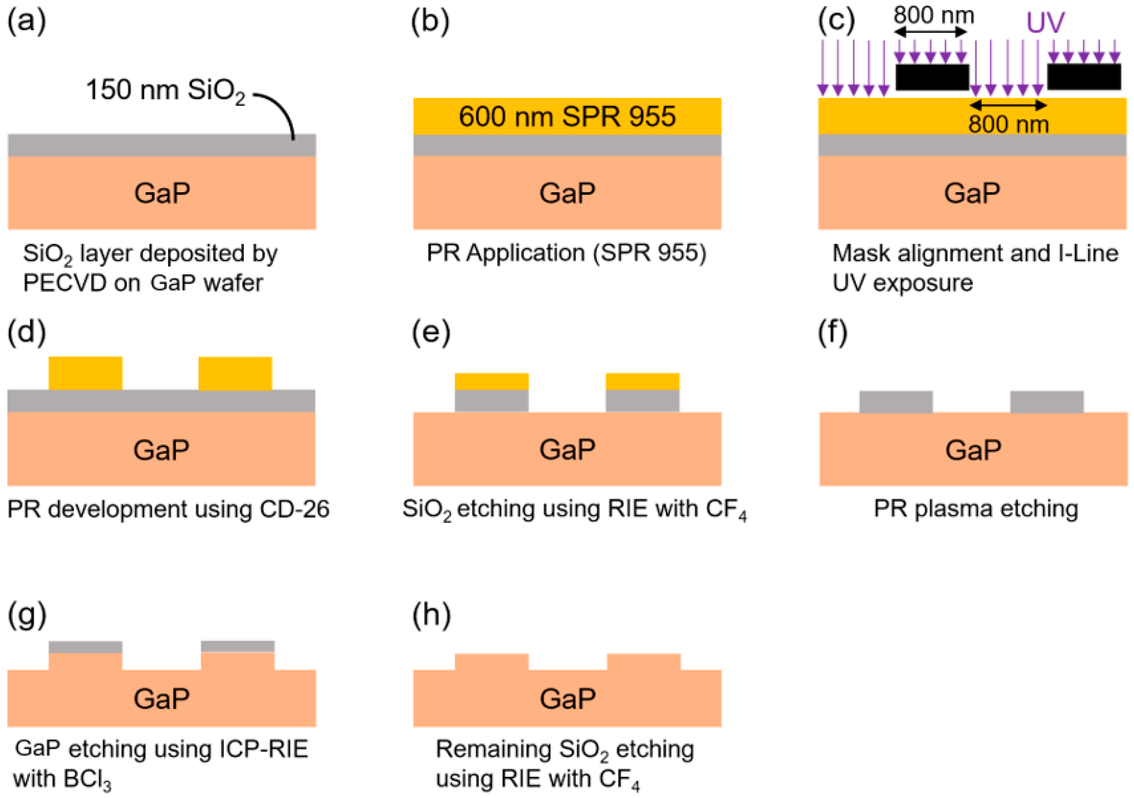
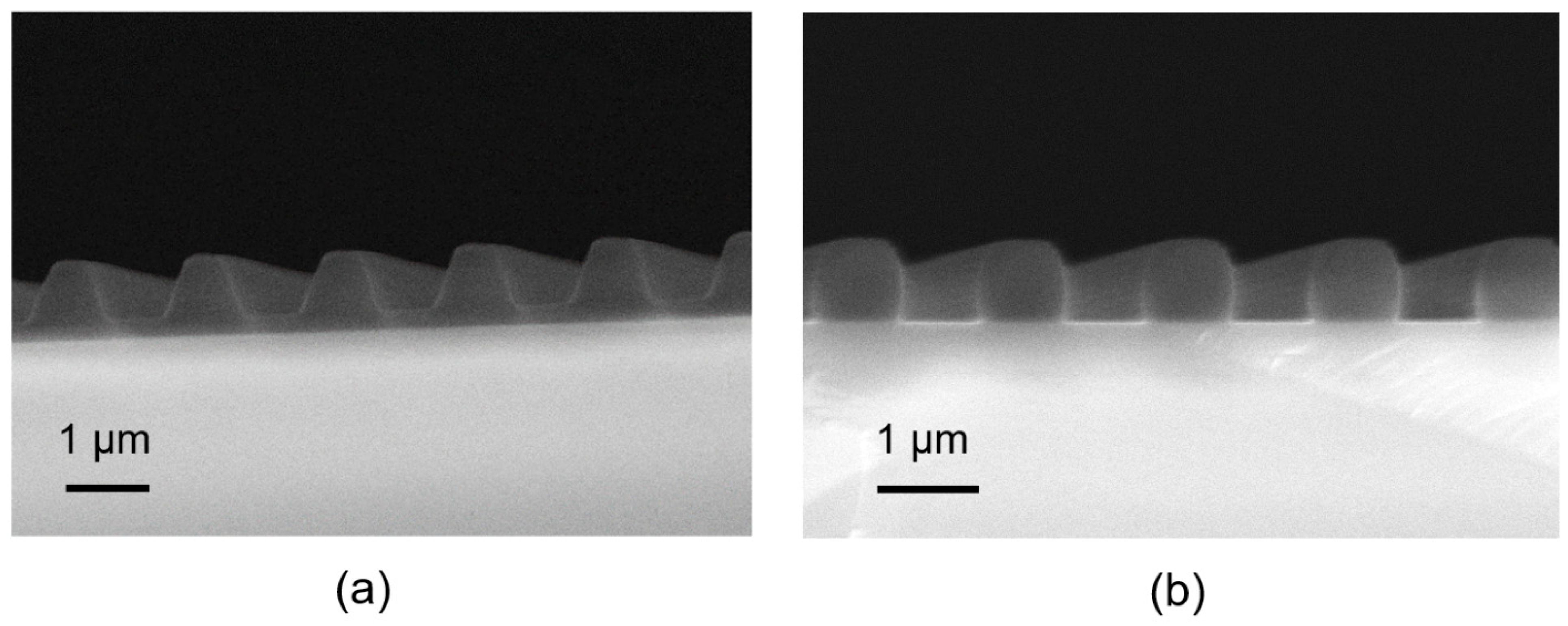
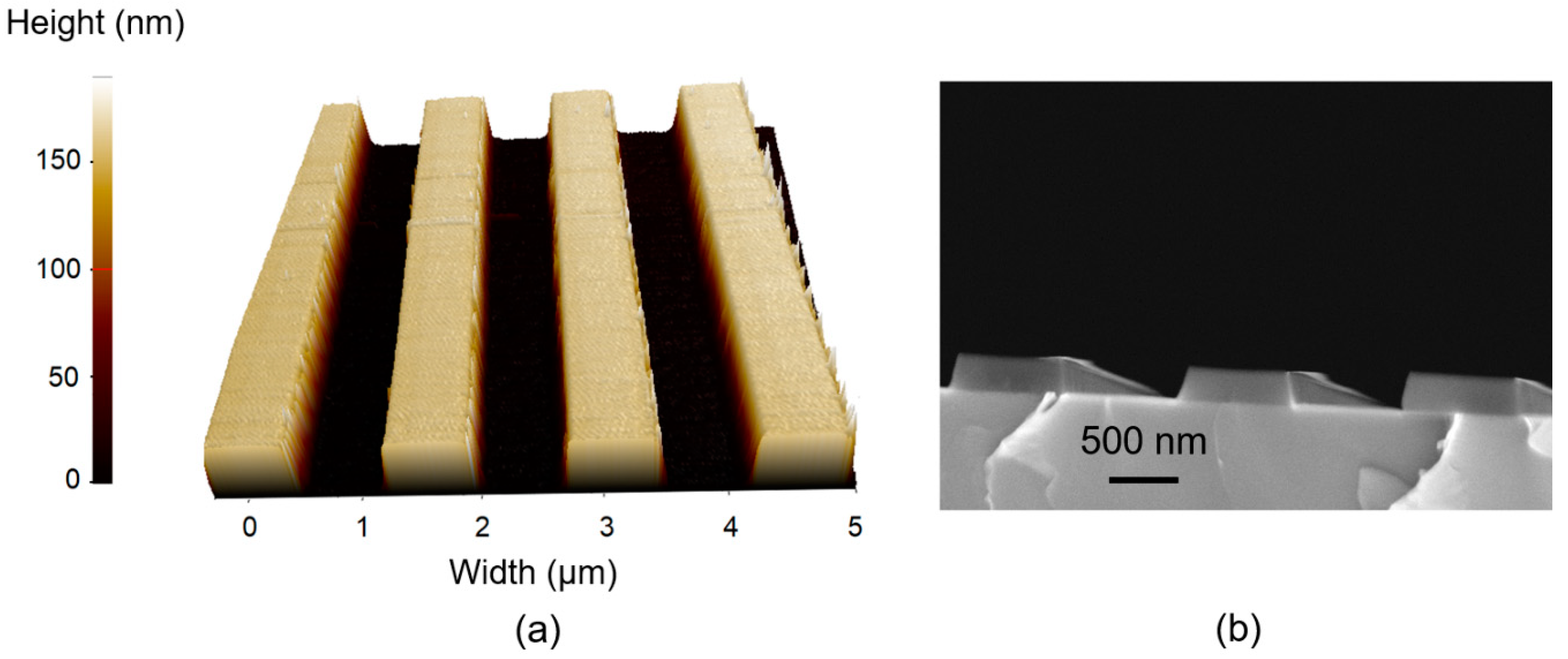
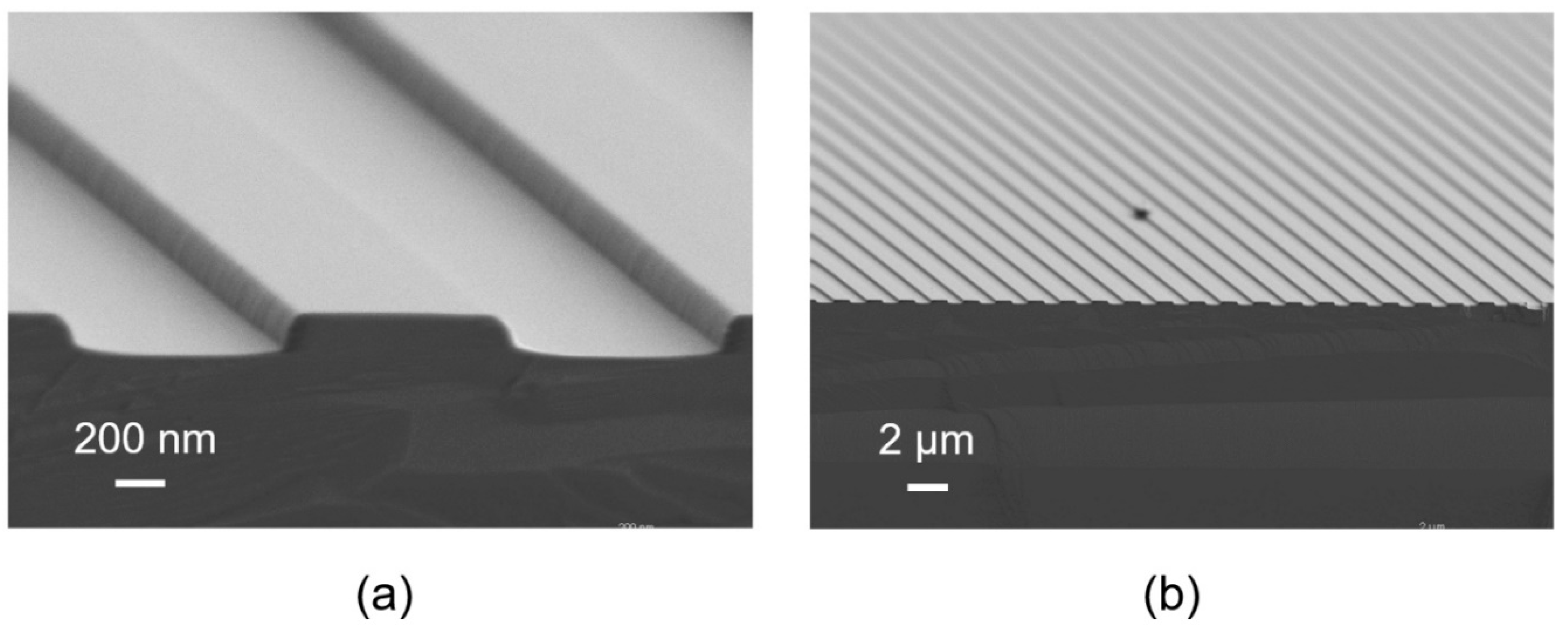
2. Fabrication Process and Results

The process flow for the nanograting fabrication shown in Figure 1 is developed for a 110-cut, nominally undoped, double-side polished, 450 µm thick, 2-inch diameter GaP wafer. The general procedure is inspired by standard Si-based photolithography, for which a spatial pattern is first optically imprinted onto the PR before being transferred to an oxide layer throughout a selective etching process. A different etching process is then used to preferentially remove the substrate material and effectively engrave the pattern up to a chosen depth. Since we control the SiO2 layer deposition and rely on dry etch processes to avoid potential chemical reactions with the substrate, our recipe, demonstrated for GaP, could be applied to a large range of materials. In this section, we describe the details of the fabrication process.
We first use a standard three-step cleaning process to remove any surface residues on the GaP wafer: (i) an acetone ultrasonic bath; (ii) an isopropyl alcohol (IPA) ultrasonic bath; and (iii) a deionized (DI) water rinse. After drying the wafer with a nitrogen blower, a 150 nm SiO2 layer is homogeneously deposited on the entire wafer surface using a plasma-enhanced chemical vapor deposition (PECVD) method. As briefly mentioned above, the SiO2 layer is etched and then acts as a mask while inductively coupled plasma-reactive ion etching (ICP-RIE) is used to locally remove the GaP material. We adopted this strategy as SiO2 exhibits a high selectivity to standard RIE processes used to etch III-V semiconductors, such as GaP. Using BCl3 gas, we observe a 3:1 etching selectivity for SiO2 on GaP. Before depositing the PR layer, the sample is first exposed to hexa-methyldisilazane (HMDS) inside a dedicated oven for 5 min at 90 °C, which creates an adhesion promoter layer between the SiO2 and the PR. The SiO2 layer forms polar OH bonds when exposed to the atmospheric humidity, which results in a hydrophilic surface. This causes low adhesion between the surface and low polar materials such as a photoresist. In order to make the surface water repellent and PR-attractive, non-polar molecules of an adhesion promoter such as HMDS can be used [39]. Spin coating deposition of the PR (MEGAPOSIT SPR 955) is performed at high rotation speed (up to 6000 rpm) to reduce the thickness and therefore optimize the pattern resolution [13,40]. We use five steps to avoid the presence of microbubbles and optimize the thickness uniformity: (1) 15 s at 200 rpm/s, increasing the speed from 0 to 3000 rpm; (2) 30 s at 3000 rpm; (3) 15 s at 200 rpm/s; (4) 30 s at 6000 rpm; (5) 30 s at −200 rpm/s, reducing the speed from 6000 rpm to 0 rpm. We obtain a 600 nm-thick positive PR approaching the minimum thickness of 500 nm specified by the manufacturer [9]. We then let the device rest for 1 min and perform a prebake for 1 min at 100 °C on a hotplate.
An Optical Associate Inc. (OAI) 200IR mask-aligner combined with two i-line filters performs UV exposure at a wavelength of 365 nm with a uniform spatial intensity distribution of 10.15 mW/cm2. Direct contact between the photomask and the substrate is used to minimize pattern deformation due to diffraction effects [40]. UV light reflected by the substrate may still induce an optical standing wave resulting from interference effects, which affects the spatial homogeneity of the structure in the vertical direction. To reduce the standing wave effect, a post-exposure bake is performed at 115 °C on a hotplate for 2 min [41]. During the PR development, the exposed regions of the photoresist are chemically etched with CD-26. This step is immediately followed by DI rinsing and nitrogen drying. We first tested a dosage of 90 mJ/cm2 and a 45 s development time, but we observed over-etching of the grating height while the photoresist did not develop properly in the exposed areas. Figure 2 compares this result to a different process yielding a square PR grating with sharp edges, which consists of a dosage of 145 mJ/cm2 and a development time of 12 s. A hard bake performed at 135 °C on a hotplate for 10 min is then used to increase the resistance of the photoresist for the up-coming RIE process, while also eliminating the photosensitivity of the PR. This allows for the sample to remain unaffected when exposed to visible light, thus allowing for characterization with an optical microscope.
In the next series of steps, the exposed areas of the SiO2 layer are etched using a SAMCO 10-NR RIE system. Hydrofluoric acid (HF) is often used to chemically etch SiO2, but here we implement the dry RIE method to avoid any potential reactions between HF and the substrate. We use a RIE power of 100 W, a CF4 gas flow of 40 standard cubic centimeters per minute (SCCM), and a chamber pressure of 3 Pa resulting in an etch rate of 30 nm/min for SiO2 and 110 nm/min for the SPR 955. A 5 min etching time is required to expose selected regions of the GaP substrate. Any leftover PR is removed with a <1 min RIE step using O2. The fabricated structure is characterized using atomic force microscopy (AFM) and scanning electron microscopy (SEM) to verify the successful transfer of the photomask pattern onto the SiO2 layer with high accuracy (Figure 3a,b).
The ICP-RIE method has been used to achieve isotropic and highly selective etching processes on semiconductors. Previous work has been reported on 8:51 and 4:10 etching selectivities using a SiO2 patterned layer on GaAs [42] and Si [43] substrates, respectively. Here, we apply this etching method with the SAMCO 110ip system using the following parameters: ICP power of 50 W, bias power of 25 W, a BCl3 gas flow of 2.5 SCCM and a chamber pressure of 0.15 Pa, resulting in a 56.5 nm/min etch rate for GaP. After a 4.2 min etch, the remaining SiO2 mask is removed by inserting the sample inside of a SAMCO 10-NR system for 3 min using a power of 100 W, a CF4 gas flow of 40 SCCM and a chamber pressure of 3 Pa. An SEM image of the resulting GaP nanogratings with periodicity of 1600 nm, width of 800 nm, length of 8 mm and height of 245 nm is shown in Figure 4. Finally the wafer is diced to 1 cm × 1 cm samples using a MTI corporation SYJ-800 dicing system allowing for easy integration into a time-resolved THz spectroscopy system.
Table 1 summarizes the details of our phase-grating fabrication process on a single GaP crystal with sub-micron features. Since the photomask pattern is first transferred to a SiO2 layer deposited on GaP before ICP-RIE, the steps presented in this work could be applied to a range of different substrates. Only modifications to the ICP-RIE parameters would then be required.

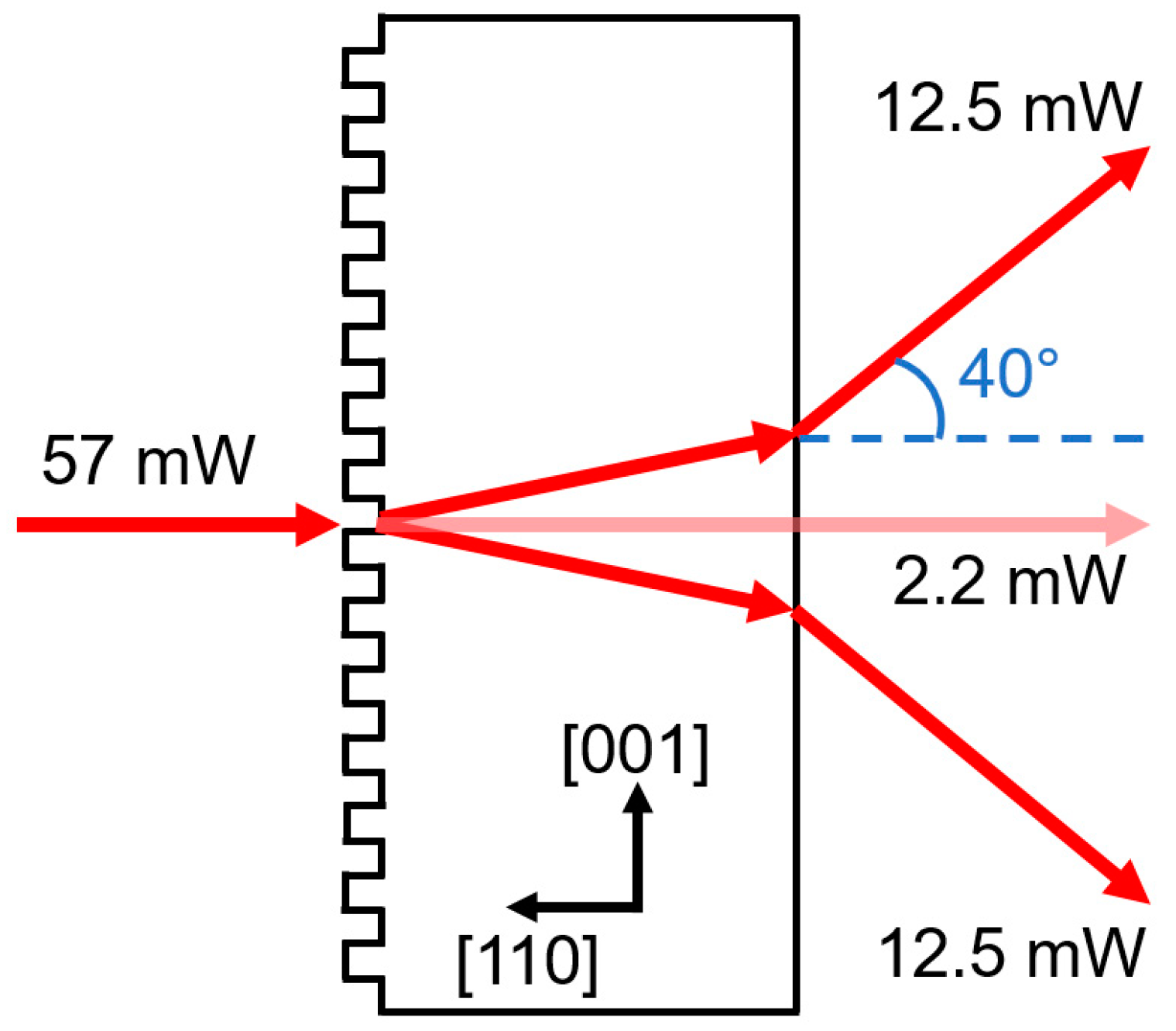
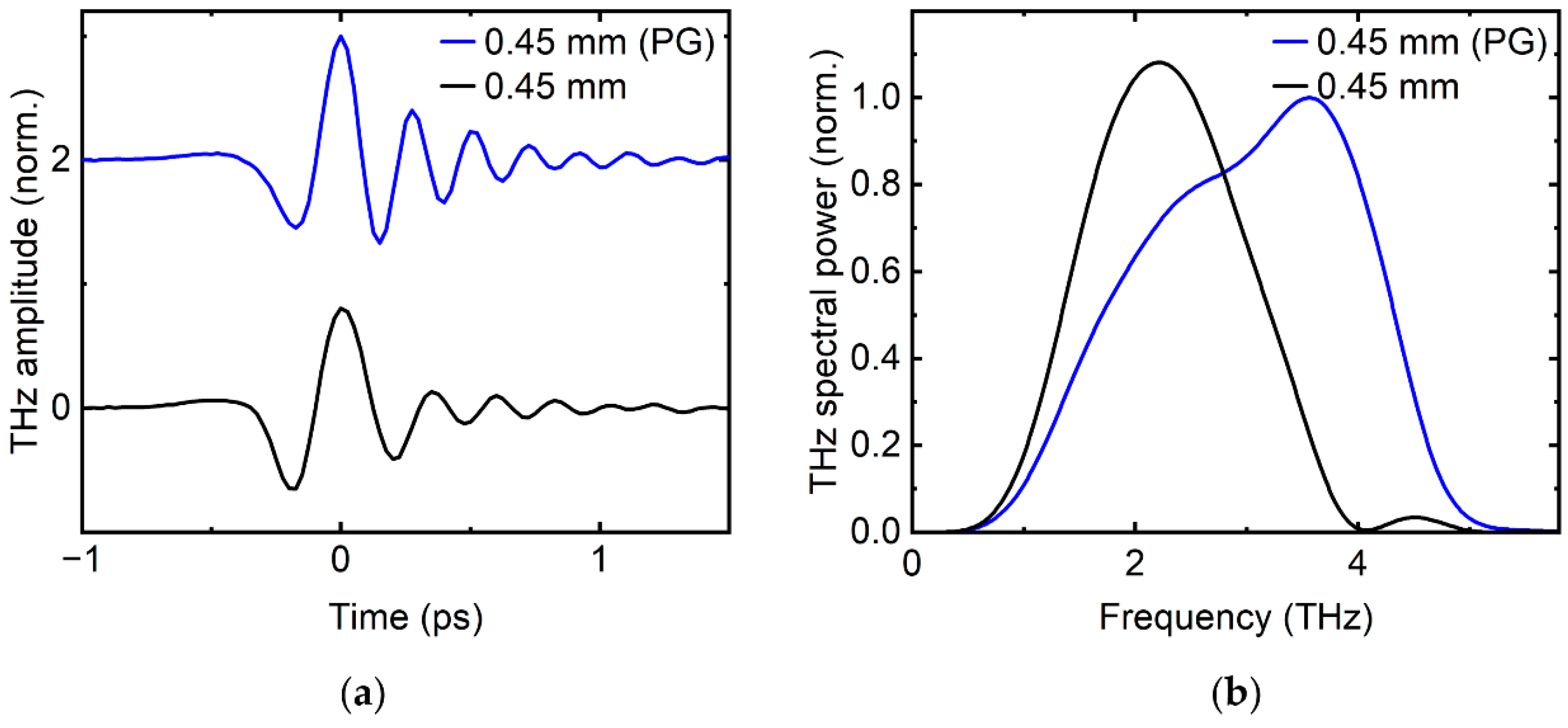
3. Optical and Terahertz Measurement

Phase-locked THz transients can be generated by optical rectification of ultrafast NIR pulses propagating inside of a second-order nonlinear crystal when phase-matching conditions are satisfied [44]. Generally, experimentalists must rely on a limited number of crystals displaying proper linear and nonlinear properties for efficient THz generation. Recently, configurations relying on a grating at the surface of the nonlinear crystal were proposed to achieve a non-collinear configuration between a diffracted NIR pulse and a generated THz wave [45,46,47]. In this scheme, the grating pitch, which determines the angles of diffraction, can be adjusted to optimize phase-matching conditions, which are otherwise fixed by the material optical properties. Recent experiments have used this configuration to demonstrate a higher THz generation efficiency at specific THz frequencies and in some cases a larger THz spectral bandwidth [6,48,49]. Those studies relied on e-beam lithography for the fabrication of the phase grating, or used a periodically patterned oxide layer as a diffractive element on the surface of the nonlinear crystal. A related optical geometry proposed by reference [50,51] relies on a simple optical configuration where the incoming NIR pulse is at normal incidence to the crystal while both positive and negative diffracted orders contribute to the generation of THz radiation. However, this scheme depends on a null zero-order phase grating made from a single crystal material to take advantage of a symmetrical redistribution of the transmitted optical energy into the two first orders of diffraction (m = −1, +1). The phase grating described in this work is designed for such a scheme and is fabricated on the surface of a GaP wafer, since this material offers advantageous phase matching conditions and a relatively high second-order nonlinear coefficient for efficient THz generation. In this section, we evaluate the grating performance using a standard time-resolved THz configuration using 60 fs NIR pulses at a repetition rate of 1.1 MHz and centered at 1030 nm to generate the THz wave by optical rectification [37]. When such an optical source is focused into a 110-oriented 450 µm-thick GaP crystal, THz is emitted with an effective spectral bandwidth limited to <3 THz frequencies due to phase matching conditions. Using the grating parameters of a 1600 nm period and a filling factor of ½, the resulting non-collinear geometry can allow for efficient THz generation around 4 THz [6].
The target height of the phase grating in GaP is 245 nm to achieve a π phase shift between the sections of the beam passing through the crests and valleys of the grating, therefore resulting in destructive interference in the transmitted 0th order of diffraction. We first characterize the performance of the diffractive optical device by observing the transmitted diffraction orders. As illustrated in Figure 5, the total power in the transmitted 0th order was measured to be approximately 4% of the incident light, while 44% was found in the 1st diffraction orders (equally distributed among m = −1 and +1). This value approaches the theoretical maximum [52] considering that 46% of the incident power is reflected at both GaP interfaces and 9% of the incident power is distributed to the 3rd diffraction orders. Our finite-difference time-domain (FDTD) simulations indicate that at the GaP front surface, the phase grating suppresses the NIR reflection by 5% when compared to a flat incident surface. Additionally, at the back surface of the crystal, there are power losses due to the Fresnel reflection. Considering the reflections of the diffracted orders inside of the crystal, we calculate the component of the transmitted power in the pure 0th order to be approximately 0.4 mW, indicating a high-quality null zero-order phase grating. We measured the first diffracted orders at an angle of 40° relative to the normal, which confirms the period of the grating to be 1600 nm. The grating is oriented along the 1 1 ¯ 0 crystal axis, or perpendicular to the 110 and 001 axes. When the incident pulse is polarized along this direction, the diffraction does not affect the projection of the optical field components onto the non-zero second-order coefficients of the crystal. This orientation ensures the same THz generation efficiency with and without the presence of the phase grating.
The time-resolved THz field amplitude generated with our grating device was measured and compared to the THz field amplitude generated inside of an unpatterned window from the same GaP wafer. In both cases, THz transients are detected with a 200 µm thick GaP crystal by standard electro-optic sampling. As shown in Figure 6, both signals have comparable peak field values in the time domain. However, their respective spectral power, obtained by squaring the Fourier transform of the time-domain data, show significant differences. The geometry based on a standard unpatterned crystal (black line) shows a THz spectrum peaking around 2 THz with a bandwidth of 2 THz while the geometry which implements the phase-grating device peaks at 3.5 THz and has a bandwidth of 3 THz. Most notably, we observe that almost half of the THz power is found at frequencies above 3 THz when the non-collinear geometry is used. The resulting spectral broadening is due to the diffraction of the incident optical pulse on the grating, which allows for the phase matching conditions to be satisfied at 4 THz [5,6]. Finally, we note that the focused NIR pulse in our experiment, with a relatively high peak intensity of 3500 GW/cm2, did not damage or degrade the performance of the surface grating.

4. Conclusions

We report on a process flow for wafer-scale fabrication of phase gratings in single-crystal GaP with sub-micron features. The concept is based on PECVD deposition of a SiO2 layer, i-line contact photolithography and RIE to transfer the pattern of a photomask to this layer, and finally ICP-RIE to etch the semiconductor. The contact i-Line photolithography method is used to transfer the nanograting image onto a GaP substrate. This method is well known for low-cost microfabrication processes and we have optimized the process parameters to reach nanoscale dimensions on a 2-inch wafer. SEM images confirm that the fabricated grating has the specified dimensions: a period of 1600 nm, a width of 800 nm and a height of 245 nm. These dimensions are also confirmed by optical diffraction experiments. We notably measure 44% of the incident optical power in the first orders of diffraction while less than 1% is in the 0th order. Furthermore, we observe that grating-assisted non-collinear optical rectification in GaP results in efficient THz generation at frequencies above 3 THz, a region generally difficult to access with time-resolved THz systems. We believe that our fabrication technique is directly applicable to a large range of materials by simply fine-tuning the last ICP-RIE procedure. Our scalable and cost-effective fabrication process relying on contact photolithography could be used for mass production of photonics and electronic devices with sub-micron features. The adoption of these types of photonic devices in the field of THz photonics will enable various nonlinear crystals to be used in a non-collinear geometry for efficient generation of THz waves at selected frequencies.

Author Contributions

Conceptualization, M.B. and W.C.; methodology, M.B.; software, M.B. and W.C.; validation, M.B., W.C. and J.-M.M.; formal analysis, M.B., W.C., A.G. and J.-M.M.; investigation, M.B., W.C. and J.-M.M.; resources, J.-M.M.; data curation, M.B. and W.C.; writing—original draft preparation, M.B.; writing—review and editing, M.B., W.C., A.G. and J.-M.M.; visualization, M.B. and W.C.; supervision, J.-M.M.; project administration, A.G. and J.-M.M.; funding acquisition, A.G. and J.-M.M. All authors have read and agreed to the published version of the manuscript.

Funding

This work was funded by the National Sciences and Engineering Research Council of Canada (NSERC) (I2IPJ 544508-19; RGPIN-2016-04797) and the University of Ottawa, NRC Joint Centre for Extreme Photonics.

Institutional Review Board Statement

Not applicable.

Informed Consent Statement

Not applicable.

Data Availability Statement

The data supporting the findings of this study are available within the article.

Acknowledgments

The authors are grateful to Kaustubh Vyas for technical assistance.

Conflicts of Interest

The authors declare no conflict of interest.

References

  1. Seisyan, R.P. Nanolithography in Microelectronics: A Review. Tech. Phys. 2011, 56, 1061–1073. [Google Scholar] [CrossRef]
  2. Ross, C.A.; Smith, H.I.; Savas, T.; Schattenburg, M.; Farhoud, M.; Hwang, M.; Walsh, M.; Abraham, M.C.; Ram, R.J. Fabrication of patterned media for high density magnetic storage. J. Vac. Sci. Technol. B Microelectron. Nanom. Struct. 1999, 17, 3168. [Google Scholar] [CrossRef]
  3. Nayak, P.K.; Mahesh, S.; Snaith, H.J.; Cahen, D. Photovoltaic Solar Cell Technologies: Analysing the State of the Art. Nat. Rev. Mater. 2019, 4, 269–285. [Google Scholar] [CrossRef]
  4. Sezer, N.; Koç, M. A Comprehensive Review on the State-of-the-Art of Piezoelectric Energy Harvesting. Nano Energy 2021, 80, 105567. [Google Scholar] [CrossRef]
  5. Halpin, A.; Cui, W.; Schiff-Kearn, A.W.; Awan, K.M.; Dolgaleva, K.; Ménard, J.-M. Enhanced Terahertz Detection Efficiency via Grating-Assisted Noncollinear Electro-Optic Sampling. Phys. Rev. Appl. 2019, 12, 31003. [Google Scholar] [CrossRef]
  6. Cui, W.; Awan, K.M.; Huber, R.; Dolgaleva, K.; Ménard, J.-M. Broadband and High-Sensitivity Time-Resolved THz System Using Grating-Assisted Tilted-Pulse-Front Phase Matching. Adv. Opt. Mater. 2022, 10, 2101136. [Google Scholar] [CrossRef]
  7. Abasahl, B.; Santschi, C.; Raziman, T.V.; Martin, O.J.F. Fabrication of Plasmonic Structures with Well-Controlled Nanometric Features: A Comparison between Lift-off and Ion Beam Etching. Nanotechnology 2021, 32, 475202. [Google Scholar] [CrossRef]
  8. Krause, B.; Pham, M.T.; Luong, H.M.; Nguyen, T.D.; Hoang, T.B. Periodic Nanohole Arrays with Enhanced Lasing and Spontaneous Emissions for Low-Cost Plasmonic Devices. ACS Appl. Nano Mater. 2022, 5, 1185–1191. [Google Scholar] [CrossRef]
  9. Northfield, H.; Krupin, O.; Tait, R.N.; Berini, P. Tri-Layer Contact Photolithography Process for High-Resolution Lift-Off. Microelectron. Eng. 2021, 241, 111545. [Google Scholar] [CrossRef]
  10. Zheng, L.; Zywietz, U.; Birr, T.; Duderstadt, M.; Overmeyer, L.; Roth, B.; Reinhardt, C. UV-LED Projection Photolithography for High-Resolution Functional Photonic Components. Microsyst. Nanoeng. 2021, 7, 64. [Google Scholar] [CrossRef]
  11. Levinson, H.J. Principles of Lithography; SPIE Press: Bellingham, MA, USA, 2005; Volume 146, ISBN 0819456608. [Google Scholar]
  12. Neisser, M. International Roadmap for Devices and Systems Lithography Roadmap. J. Micro/Nanopatterning Mater. Metrol. 2021, 20, 044601. [Google Scholar] [CrossRef]
  13. Stuerzebecher, L.; Fuchs, F.; Zeitner, U.D.; Tuennermann, A. High-Resolution Proximity Lithography for Nano-Optical Components. Microelectron. Eng. 2015, 132, 120–134. [Google Scholar] [CrossRef]
  14. van Assenbergh, P.; Meinders, E.; Geraedts, J.; Dodou, D. Nanostructure and Microstructure Fabrication: From Desired Properties to Suitable Processes. Small 2018, 14, 1703401. [Google Scholar] [CrossRef] [PubMed]
  15. Wu, C.-Y.; Hsieh, H.; Lee, Y.-C. Contact Photolithography at Sub-Micrometer Scale Using a Soft Photomask. Micromachines 2019, 10, 547. [Google Scholar] [CrossRef] [Green Version]
  16. Samoila, C.; Ursutiu, D.; Tavkhelidze, A.; Jangidze, L.; Taliashvili, Z.; Skhiladze, G.; Tierean, M. Nanograting Layers of Si. Nanotechnology 2020, 31, 035301. [Google Scholar] [CrossRef]
  17. Qiao, W.; Pu, D.; Chen, L.-S. Nanofabrication Toward High-Resolution and Large Area. In Proceedings of the 2021 IEEE 34th International Conference on Micro Electro Mechanical Systems (MEMS), Gainesville, FL, USA, 25–29 January 2021; pp. 42–46. [Google Scholar]
  18. Tallents, G.; Wagenaars, E.; Pert, G. Lithography at EUV Wavelengths. Nat. Photonics 2010, 4, 809–811. [Google Scholar] [CrossRef]
  19. Levenson, M.D.; Viswanathan, N.S.; Simpson, R.A. Improving Resolution in Photolithography with a Phase-Shifting Mask. IEEE Trans. Electron Devices 1982, 29, 1828–1836. [Google Scholar] [CrossRef]
  20. Luo, R. Optical Proximity Correction Using a Multilayer Perceptron Neural Network. J. Opt. 2013, 15, 75708. [Google Scholar] [CrossRef]
  21. Sugawara, M.; Chiba, A.; Nishiyama, I. Effect of Incident Angle of Off-Axis Illumination on Pattern Printability in Extreme Ultraviolet Lithography. J. Vac. Sci. Technol. B Microelectron. Nanom. Struct. Process. Meas. Phenom. 2003, 21, 2701–2705. [Google Scholar] [CrossRef]
  22. Voelkel, R.; Vogler, U.; Bich, A.; Pernet, P.; Weible, K.J.; Hornung, M.; Zoberbier, R.; Cullmann, E.; Stuerzebecher, L.; Harzendorf, T.; et al. Advanced Mask Aligner Lithography: New Illumination System. Opt. Express 2010, 18, 20968. [Google Scholar] [CrossRef]
  23. Kim, Y.U.; Kwon, N.Y.; Park, S.H.; Kim, C.W.; Chau, H.D.; Hoang, M.H.; Cho, M.J.; Choi, D.H. Patterned Sandwich-Type Silver Nanowire-Based Flexible Electrode by Photolithography. ACS Appl. Mater. Interfaces 2021, 13, 61463–61472. [Google Scholar] [CrossRef] [PubMed]
  24. Liu, Z.; Yang, Z.; Wang, W.; Yang, Q.; Han, Q.; Ma, D.; Cheng, H.; Lin, Y.; Zheng, J.; Liu, W. Numerical and Experimental Exploration towards a 26% Efficiency Rear-Junction n-Type Silicon Solar Cell with Front Local-Area and Rear Full-Area Polysilicon Passivated Contacts. Sol. Energy 2021, 221, 1–9. [Google Scholar] [CrossRef]
  25. Yang, J.; Lin, Y.-S. Design of Tunable Terahertz Metamaterial Sensor with Single-and Dual-Resonance Characteristic. Nanomaterials 2021, 11, 2212. [Google Scholar] [CrossRef]
  26. Laguna, A.P.; Karatsu, K.; Thoen, D.J.; Murugesan, V.; Buijtendorp, B.T.; Endo, A.; Baselmans, J.J.A. Terahertz Band-Pass Filters for Wideband Superconducting On-Chip Filter-Bank Spectrometers. IEEE Trans. Terahertz Sci. Technol. 2021, 11, 635–646. [Google Scholar] [CrossRef]
  27. Nikolaidou, K.; Oliveira, H.M.; Cardoso, S.; Freitas, P.P.; Chu, V.; Conde, J.P. Monolithic Integration of Multi-Spectral Optical Interference Filter Array on Thin Film Amorphous Silicon Photodiodes. IEEE Sens. J. 2022, 22, 5636–5643. [Google Scholar] [CrossRef]
  28. Jonker, D.; Jafari, Z.; Winczewski, J.P.; Eyovge, C.; Berenschot, J.W.; Tas, N.R.; Gardeniers, J.G.E.; De Leon, I.; Susarrey-Arce, A. A Wafer-Scale Fabrication Method for Three-Dimensional Plasmonic Hollow Nanopillars. Nanoscale Adv. 2021, 3, 4926–4939. [Google Scholar] [CrossRef]
  29. Liu, G.-S.; Wang, T.; Wang, Y.; Zheng, H.; Chen, Y.; Zeng, Z.; Chen, L.; Chen, Y.; Yang, B.-R.; Luo, Y. One-Step Plasmonic Welding and Photolithographic Patterning of Silver Nanowire Network by UV-Programable Surface Atom Diffusion. Nano Res. 2021, 15, 2582–2591. [Google Scholar] [CrossRef]
  30. Yoo, D.; Barik, A.; de Leon-Perez, F.; Mohr, D.A.; Pelton, M.; Martín-Moreno, L.; Oh, S.-H. Plasmonic Split-Trench Resonator for Trapping and Sensing. ACS Nano 2021, 15, 6669–6677. [Google Scholar] [CrossRef]
  31. Yang, J.; Wang, C. Efficient Terahertz Generation Scheme in a Thin-Film Lithium Niobate-Silicon Hybrid Platform. Opt. Express 2021, 29, 16477–16486. [Google Scholar] [CrossRef]
  32. Dong, T.; Li, S.; Manjappa, M.; Yang, P.; Zhou, J.; Kong, D.; Quan, B.; Chen, X.; Ouyang, C.; Dai, F. Nonlinear THz-Nano Metasurfaces. Adv. Funct. Mater. 2021, 31, 2100463. [Google Scholar] [CrossRef]
  33. Wang, P.; Hu, R.; Huang, X.; Wang, T.; Hu, S.; Hu, M.; Xu, H.; Li, X.; Liu, K.; Wang, S. Terahertz Chiral Metamaterials Enabled by Textile Manufacturing. Adv. Mater. 2022, 34, 2110590. [Google Scholar] [CrossRef] [PubMed]
  34. Václavík, J.; Vápenka, D. Gallium Phosphide as a Material for Visible and Infrared Optics. EPJ Web Conf. 2013, 48, 28. [Google Scholar] [CrossRef] [Green Version]
  35. Martin, A.; Combrié, S.; de Rossi, A.; Beaudoin, G.; Sagnes, I.; Raineri, F. Nonlinear Gallium Phosphide Nanoscale Photonics. Photonics Res. 2018, 6, B43–B49. [Google Scholar] [CrossRef]
  36. Wilson, D.J.; Schneider, K.; Hönl, S.; Anderson, M.; Baumgartner, Y.; Czornomaz, L.; Kippenberg, T.J.; Seidler, P. Integrated gallium phosphide nonlinear photonics. Nat. Photonics 2020, 14, 57–62. [Google Scholar] [CrossRef] [Green Version]
  37. Cui, W.; Schiff-Kearn, A.W.; Zhang, E.; Couture, N.; Tani, F.; Novoa, D.; Russell, P.S.J.; Ménard, J.-M. Broadband and TunableTime-Resolved THz System Using Argon-Filled Hollow-Core Photonic Crystal Fiber. APL Photonics 2018, 3, 111301. [Google Scholar] [CrossRef] [Green Version]
  38. Paradis, C.; Drs, J.; Modsching, N.; Razskazovskaya, O.; Meyer, F.; Kränkel, C.; Saraceno, C.J.; Wittwer, V.J.; Südmeyer, T. Broadband terahertz pulse generation driven by an ultrafast thin-disk laser oscillator. Opt. Express 2018, 26, 26377–26384. [Google Scholar] [CrossRef] [Green Version]
  39. Yeh, W.-M.; Lawson, R.A.; Tolbert, L.M.; Henderson, C.L. A Study of Reactive Adhesion Promoters and Their Ability to Mitigate Pattern Collapse in Thin Film Lithography. In Proceedings of the Advances in Resist Materials and Processing Technology XXVIII, SPIE Advanced Lithography, San Jose, CA, USA, 27 February–3 March 2011; Volume 7972, pp. 534–540. [Google Scholar]
  40. Partel, S.; Kasemann, S.; Choleva, P.; Dincer, C.; Kieninger, J.; Urban, G.A. Novel Fabrication Process for Sub-Micron Interdigitated Electrode Arrays for Highly Sensitive Electrochemical Detection. Sensors Actuators B Chem. 2014, 205, 193–198. [Google Scholar] [CrossRef]
  41. Toukhy, M.A.; Hansen, S.G. Influence of Post Exposure Bake on Resist Contrast. In Proceedings of the Advances in Resist Technology and Processing XI, SPIE’S 1994 Symposium on Microlithography, San Jose, CA, USA, 27 February–4 March 1994; Volume 2195, pp. 640–651. [Google Scholar]
  42. Booker, K.; Mayon, Y.O.; Jones, C.; Stocks, M.; Blakers, A. Deep, Vertical Etching for GaAs Using Inductively Coupled Plasma/Reactive Ion Etching. J. Vac. Sci. Technol. B 2020, 38, 012206. [Google Scholar] [CrossRef]
  43. Nakayama, D.; Wada, A.; Kubota, T.; Bruce, R.; Martin, R.M.; Haass, M.; Fuller, N.; Samukawa, S. Highly Selective Silicon Nitride Etching to Si and SiO2 for a Gate Sidewall Spacer Using a CF3I/O2/H2 Neutral Beam. J. Phys. D. Appl. Phys. 2013, 46, 205203. [Google Scholar] [CrossRef]
  44. Boyd, R.W. Nonlinear Optics; Academic Press: Cambridge, MA, USA, 2020; ISBN 0128110031. [Google Scholar]
  45. Pálfalvi, L.; Fülöp, J.A.; Almási, G.; Hebling, J. Novel Setups for Extremely High Power Single-Cycle Terahertz Pulse Generation by Optical Rectification. Appl. Phys. Lett. 2008, 92, 171107. [Google Scholar] [CrossRef]
  46. Nagashima, K.; Kosuge, A. Design of Rectangular Transmission Gratings Fabricated in LiNbO3 for High-Power Terahertz-Wave Generation. Jpn. J. Appl. Phys. 2010, 49, 122504. [Google Scholar] [CrossRef]
  47. Ollmann, Z.; Fülöp, J.A.; Hebling, J.; Almási, G. Design of a high-energy terahertz pulse source based on ZnTe contact grating. Optics Commun. 2014, 315, 159. [Google Scholar] [CrossRef]
  48. Yoshida, F.; Nagashima, K.; Tsubouchi, M.; Maruyama, M.; Ochi, Y. THz pulse generation using a contact grating device composed of TiO2 /SiO2 thin films on LiNbO3 crystal. J. Appl. Phys. 2016, 120, 183103. [Google Scholar] [CrossRef]
  49. Fülöp, J.A.; Polónyi, G.; Monoszlai, B.; Andriukaitis, G.; Balciunas, T.; Pugzlys, A.; Arthur, G.; Baltuska, A.; Hebling, J. Highly efficient scalable monolithic semiconductor terahertz pulse source. Optica 2016, 3, 1075. [Google Scholar] [CrossRef] [Green Version]
  50. Bakunov, M.I.; Bodrov, S.B. Terahertz generation with tilted-front laser pulses in a contact-grating scheme. J. Opt. Soc. Am. B 2014, 31, 2549. [Google Scholar] [CrossRef]
  51. Nugraha, P.S.; Krizsán, G.; Polónyi, G.; Mechler, M.I.; Hebling, J.; Tóth, G.; Fülöp, J.A. Efficient semiconductor multicycle terahertz pulse source. J. Phys. B At. Mol. Opt. Phys. 2018, 51, 94007. [Google Scholar] [CrossRef]
  52. Harvey, J.E.; Pfisterer, R.N. Understanding diffraction grating behavior: Including conical diffraction and Rayleigh anomalies from transmission gratings. Opt. Eng. 2019, 58, 087105. [Google Scholar] [CrossRef]
Figure 1. Eight step fabrication process of a phase grating from a single GaP crystal. (a) SiO2 layer deposition using PECVD on GaP Substrate, (b) PR Application (SPR 955), (c) Mask alignment and I-Line UV exposure, (d) PR development using CD-26, (e) SiO2 etching using RIE with CF4, (f) PR plasma etching (g) GaP etching using ICP-RIE with BCl3 (h) Etching of the remaining SiO2 using RIE with CF4.
Crystals 12 00684 g001
Figure 2. SEM image of photoresist structure (a) exposure dose of 90 mJ/cm2 and development time of 45 s, and (b) exposure dose of 145 mJ/cm2 and development time of 12 s.
Crystals 12 00684 g002
Figure 3. (a) AFM image of SiO2 grating on GaP with periodicity of 1600 nm, width of 800 nm and depth of 150 nm, and (b) SEM image of SiO2 grating on GaP periodicity of 1600 nm, width of 800 nm and depth of 150 nm.
Crystals 12 00684 g003
Figure 4. SEM images of GaP nanograting (periodicity—1600 nm; width—800 nm; length—8 mm; depth—245 nm) after ICP-RIE etching on (a) a 200 nm scale and (b) a 2 µm scale.
Crystals 12 00684 g004
Figure 5. Diagram of the diffraction efficiency of the phase grating measured with laser pulses centered at 1030 nm. The transmitted 1st orders of diffraction (m = −1 and +1) are measured at an angle of 40° corresponding to a period of 1600 nm and contain 44% of the incident light. The grating is written along the direction perpendicular to the 110 and 001 crystal axes of GaP.
Crystals 12 00684 g005
Figure 6. (a) The THz field amplitude is measured in the time domain using two different generation crystals: a flat 0.45 mm-thick GaP window (black line) and the same crystal with a phase grating (PG) on its incident surface (blue line). (b) The THz spectral power calculated from the time-domain data is broader and shifted to higher THz frequencies when we use the crystal with the surface phase grating (blue line).
Crystals 12 00684 g006
Table 1. The process flow to fabricate a phase grating of a single GaP substrate with sub-micron features.
StepDescriptionDetails
1Wafer cleaningCleaning with acetone, IPA, and DI water in ultrasonic bath.
2SiO2 deposition150 nm SiO2 deposition by PECVD system at 300 °C.
3Apply HMDS layerHMDS vapor deposition in oven at 90 °C during 5 min.
4SPR955 applicationSpin coating of photoresist (15 s at 200 r/s) + (30 s at 3000 rpm) + (15 s at 200 r/s) + (30 s at 6000 rpm) + (30 s at −200 rpm/s, reducing the speed from 6000 rpm to 0 rpm).
5Prebake1 min at 100 °C on hotplate.
6UV exposure145 mJ/cm2 dosage with i-line
7Post exposure bake2 min at 115 °C on hotplate
8Photoresist development12 s in CD-26 followed by DI water bath and nitrogen blow dry.
9Hardening bake10 min at 135 °C on hotplate
10RIE of SiO2SAMCO 10-NR: CF4: 40 SCCM, power: 100 W, pressure: 3 Pa, time: 5 min
11Photoresist stripping10 SCCM, power: 25 W, pressure: 5 pa, time: 10 min
12ICP-RIE of GaP nanogratingSAMCO 110ip: BCl3: 2.5 SCCM, ICP power: 50 W, bias power: 25 W, Pressure: 0.15 Pa, temperature: 25 °C, time: 4 min 20 s
13Etching remained SiO2 by RIESAMCO 10-NR: CF4: 40 SCCM, power: 100 W, pressure: 3 Pa, time:3 min
14Dicing the waferDicing the wafer to obtain desired sample sizes
Publisher’s Note: MDPI stays neutral with regard to jurisdictional claims in published maps and institutional affiliations.

