
Processes of the Reliability and Degradation Mechanism of High-Power Semiconductor Lasers


 ,
, 

 ,
,  ,
, 

Abstract
:1. Introduction
2. Failure Mechanism
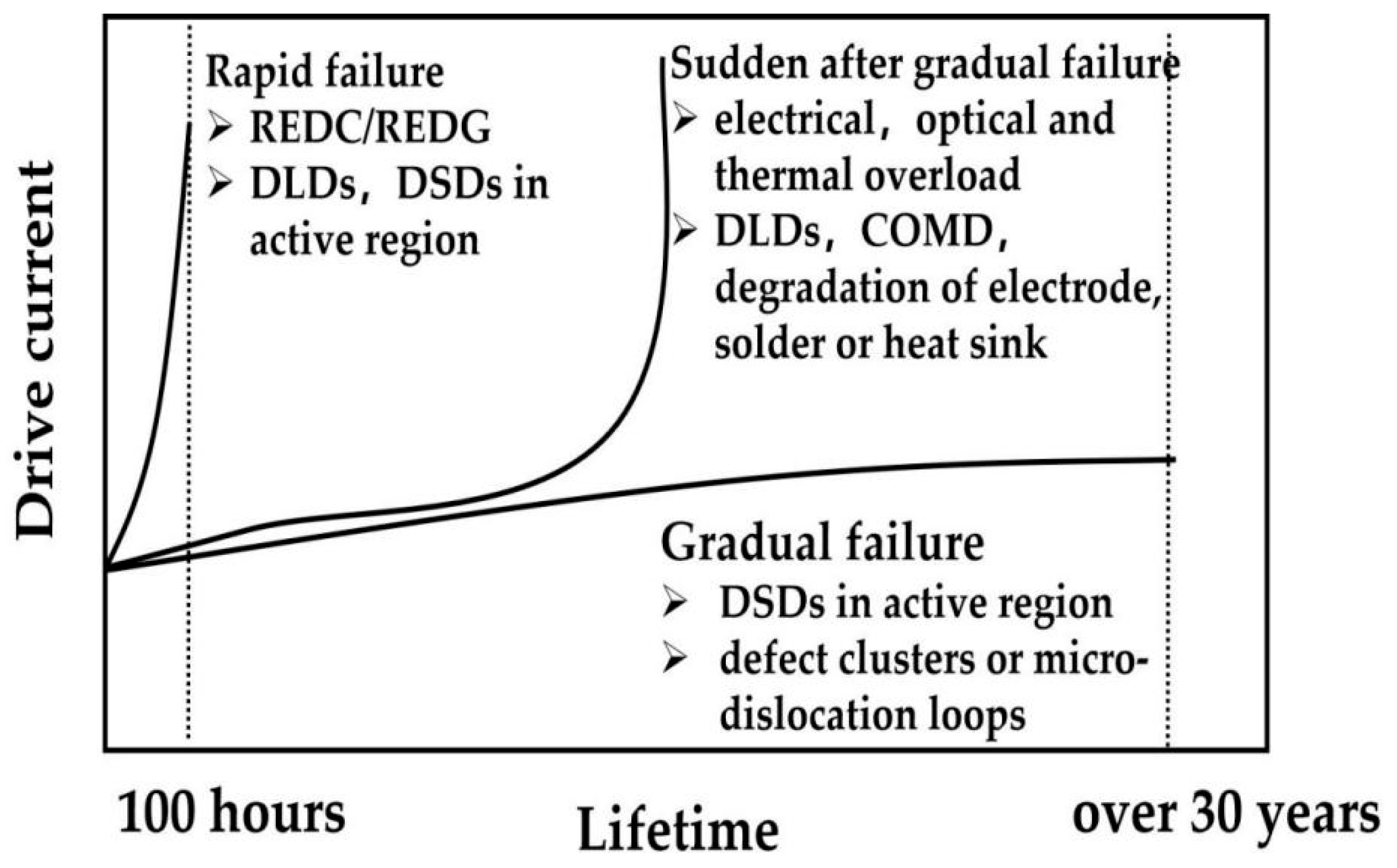
2.1. Failure Mode
2.1.1. Rapid Failure
2.1.2. Gradual Failure
2.1.3. Sudden Failure after Gradual Failure
2.2. Reasons for Degradation
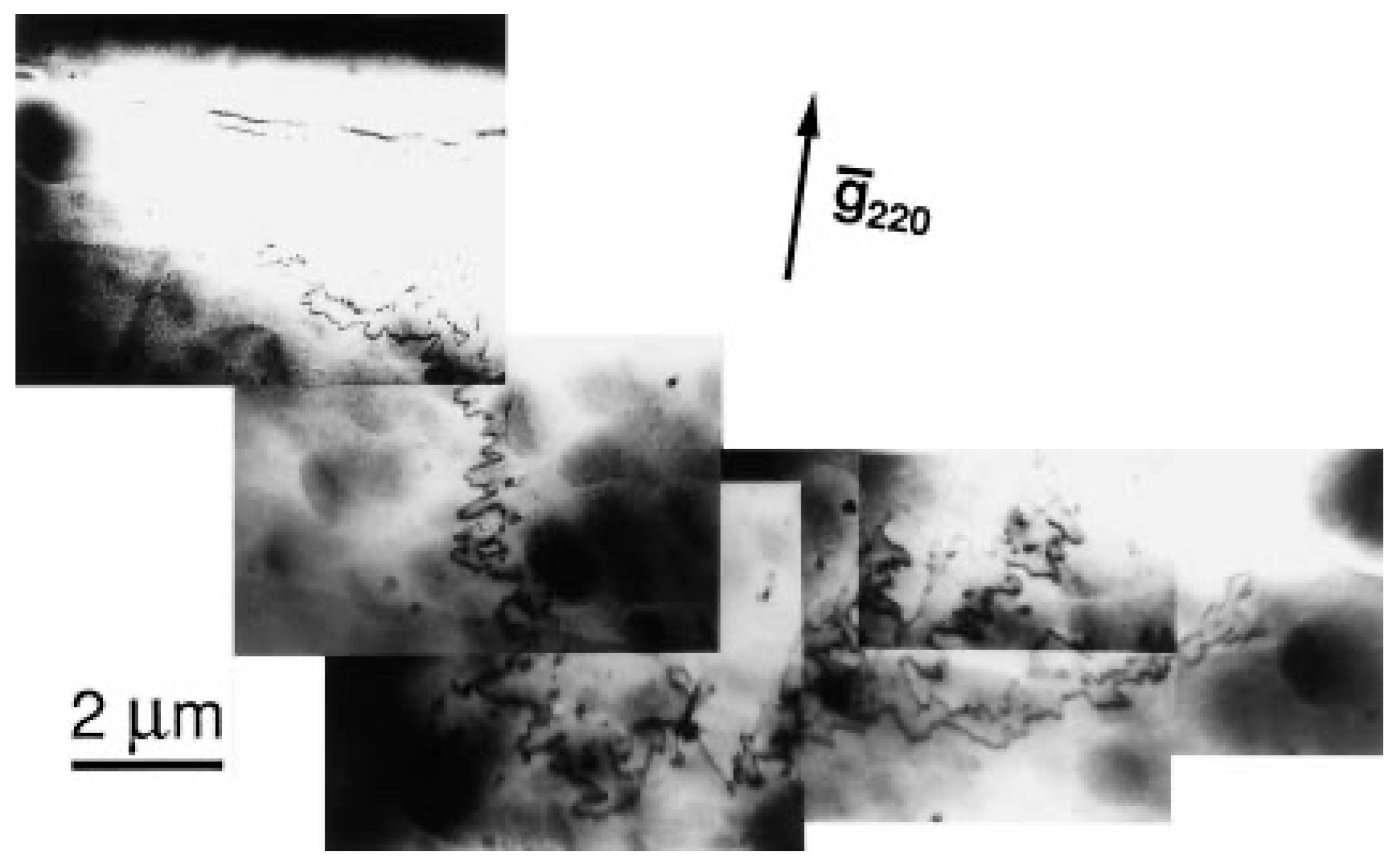
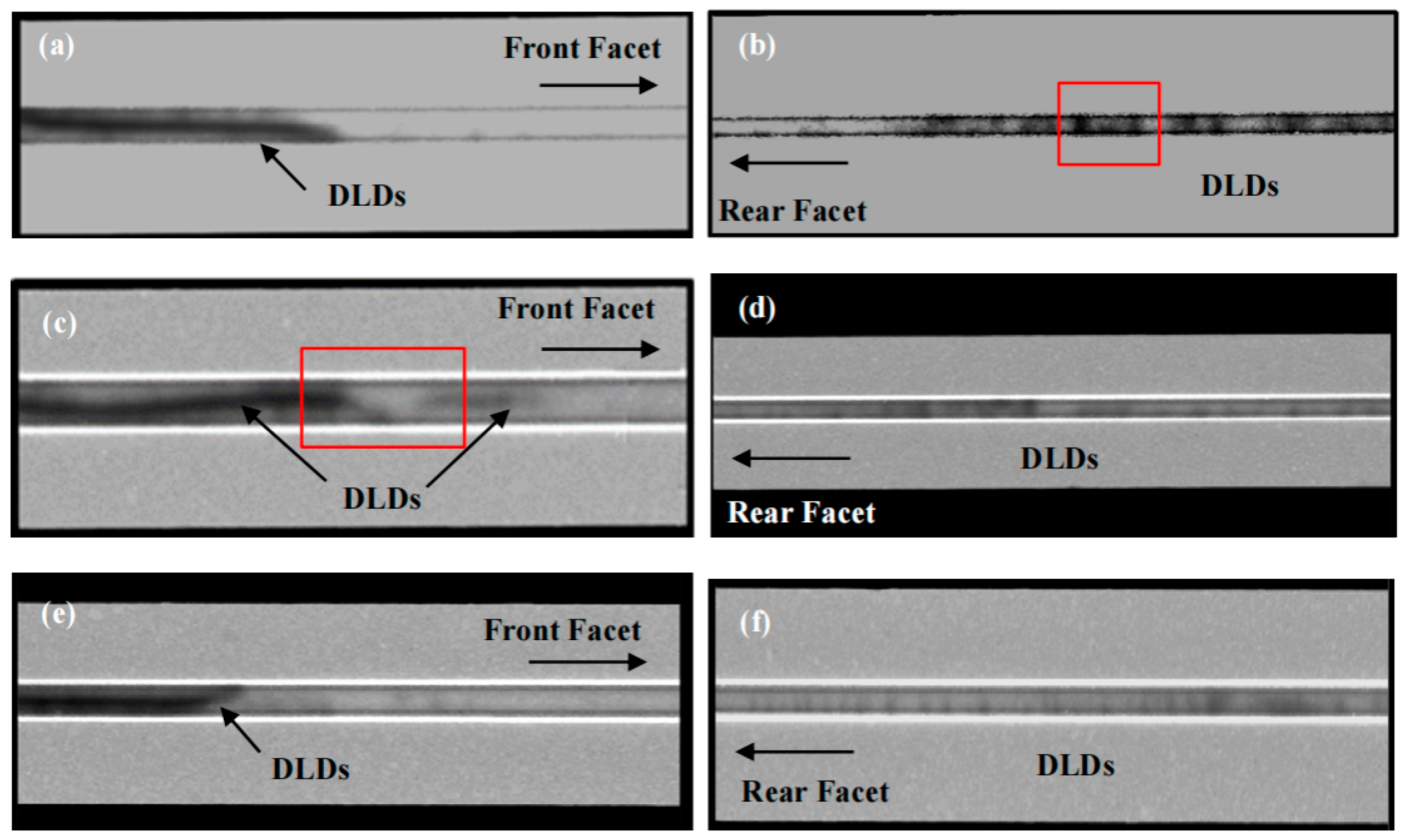
2.2.1. Internal Degradation
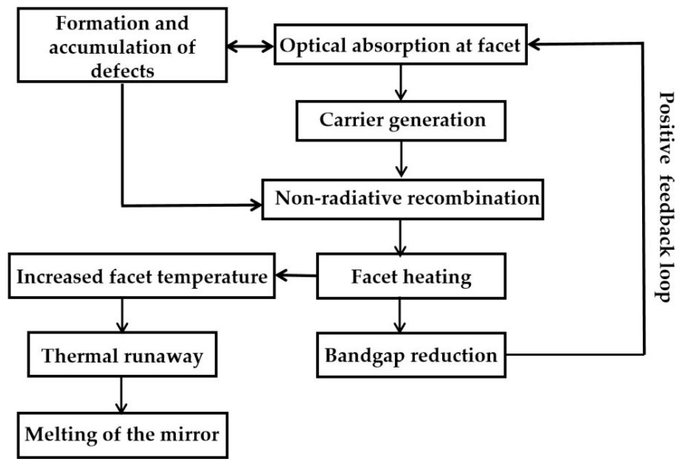
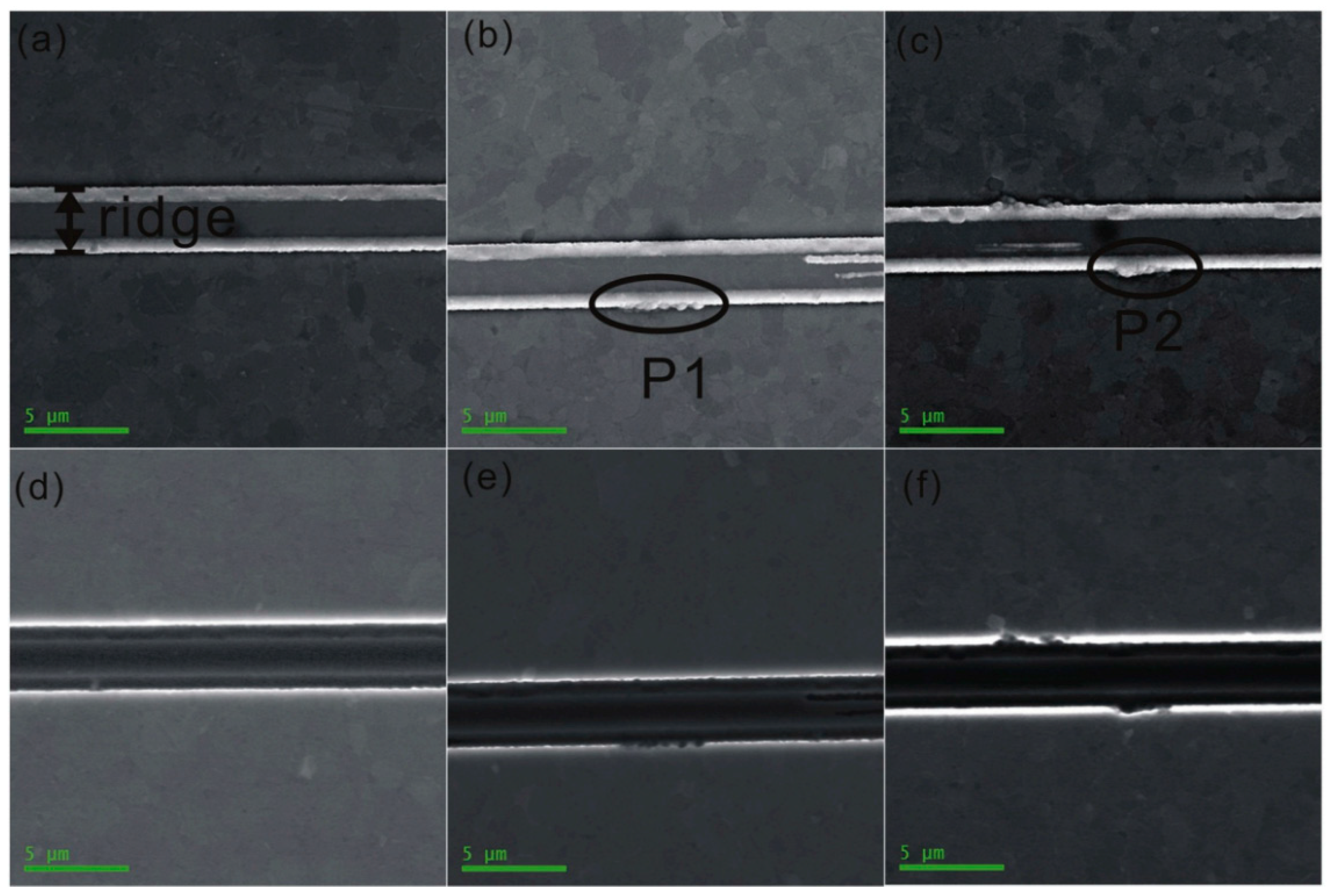
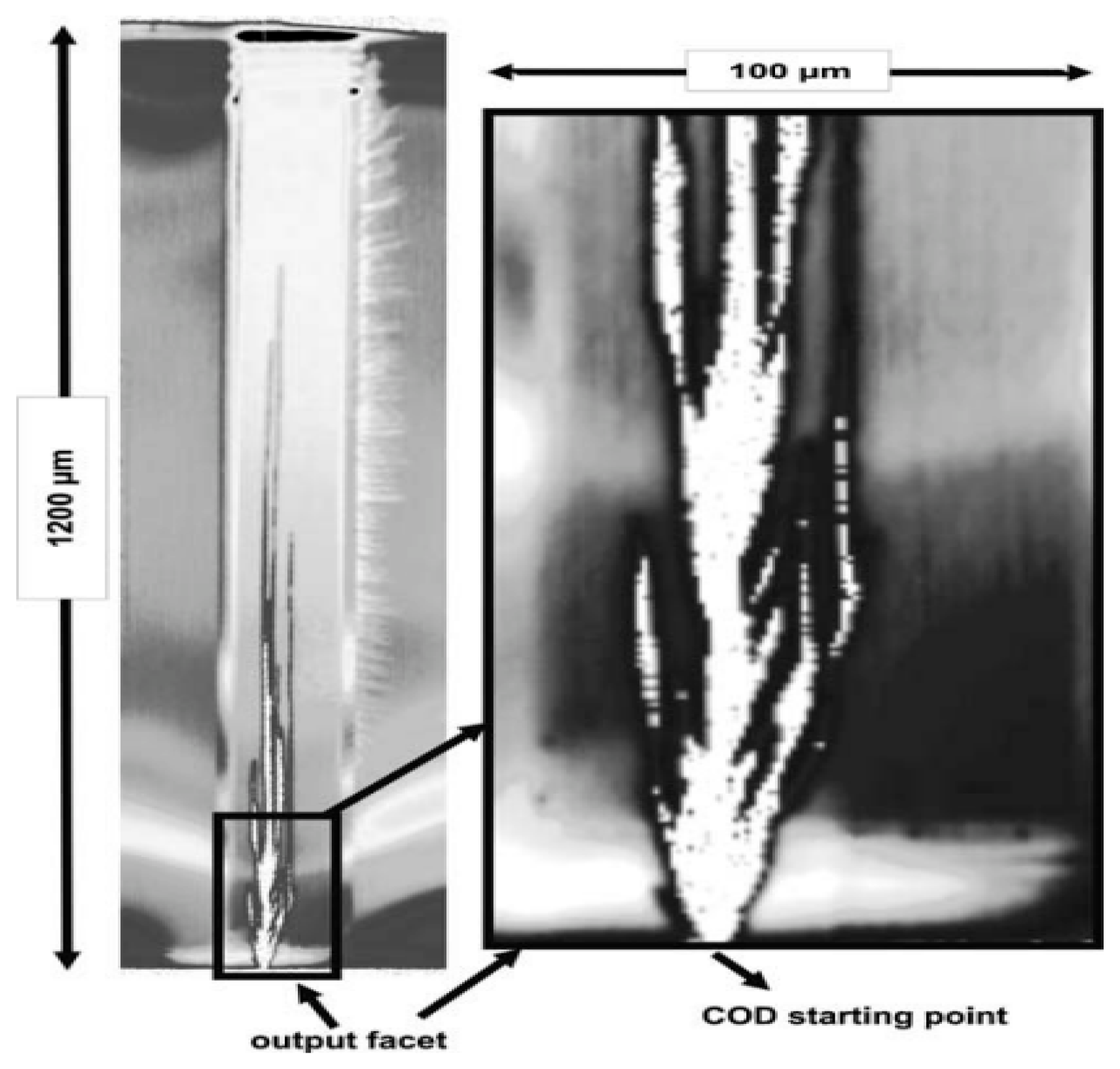
2.2.2. Mirror Facet Degradation
2.2.3. Electrode Degradation
2.2.4. Packaging-Related Degradation
2.2.5. Influence of Environmental Factors
3. Accelerated Aging Test and Lifetime Test Method
3.1. Reliability
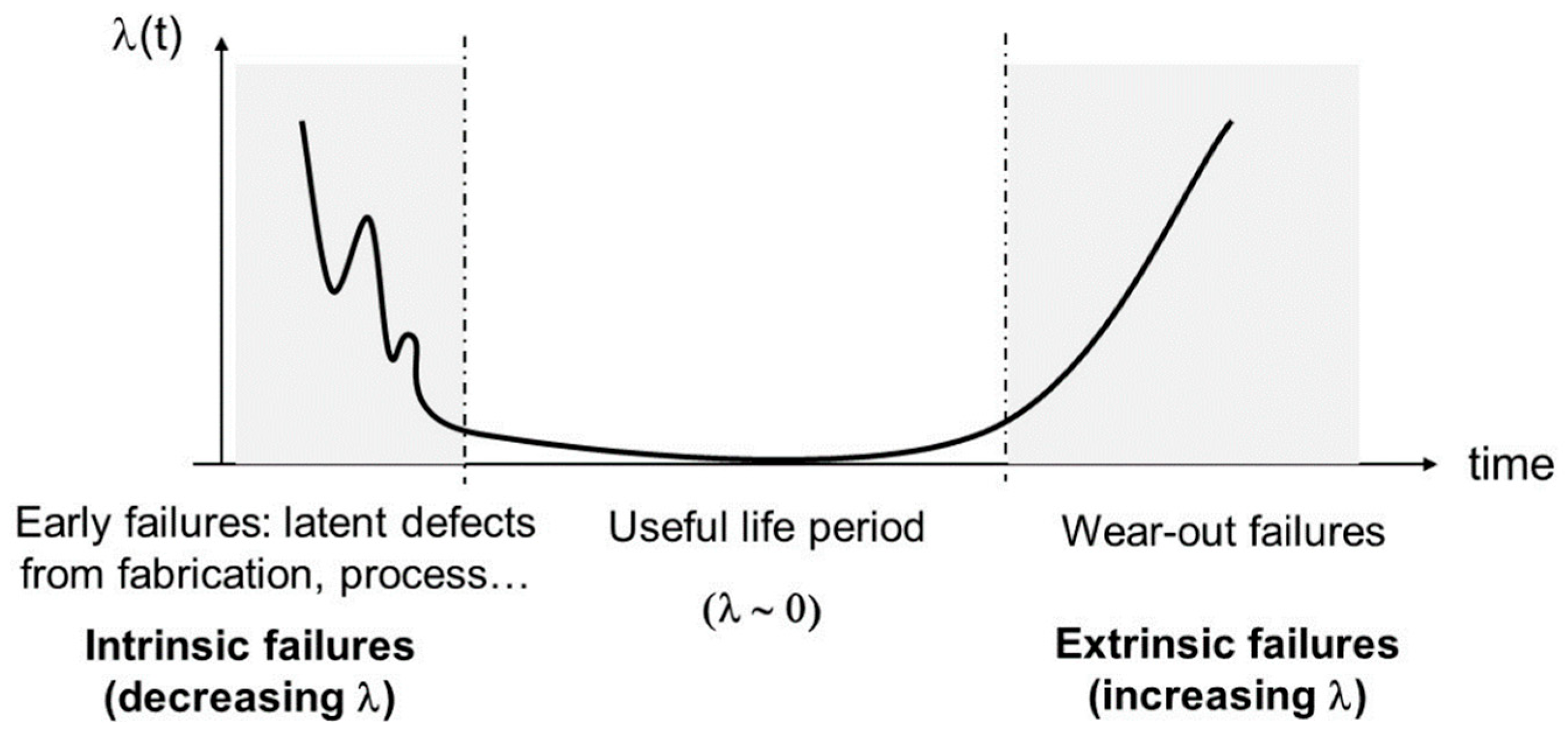
3.1.1. Reliability Overview
- (1)
- Early failure: The device has a high failure rate and a very short operating lifetime, usually due to rapid degradation caused by the rapid growth of the internal defects within the device. These defects are mainly generated during the manufacturing process.
- (2)
- Random failure: This stage has a low failure rate, is difficult or impossible to predict, and is associated with chance factors.
- (3)
- Wear and tear failure: The device shows wear and ages in different operating environments, reaching its service life, and eventually failing.
3.1.2. Reliability Experiments
3.2. Accelerated Aging Experiment
3.2.1. Theoretical Basis for the Accelerated Aging Test
Arrhenius Model
Inverse Power Law Model
3.2.2. Classification of Accelerated Aging Test
3.3. Example of Accelerated Aging Test
4. Failure Analysis Techniques
4.1. EBIC
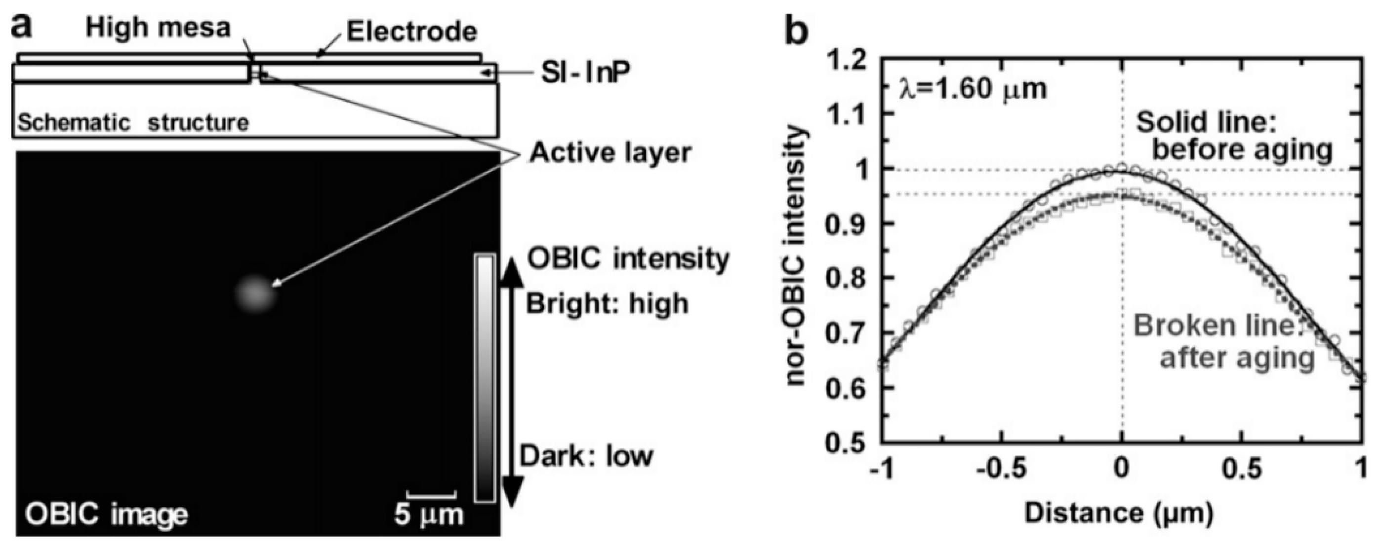
4.2. OBIC
4.3. TIVA
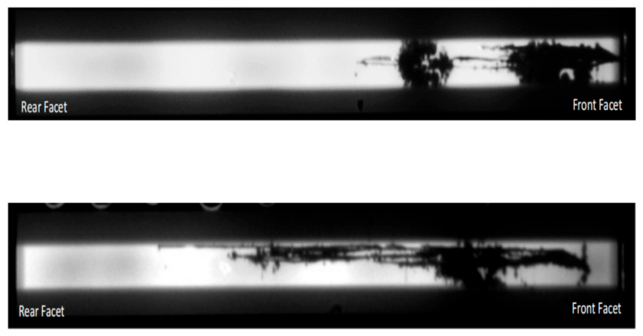
4.4. EL
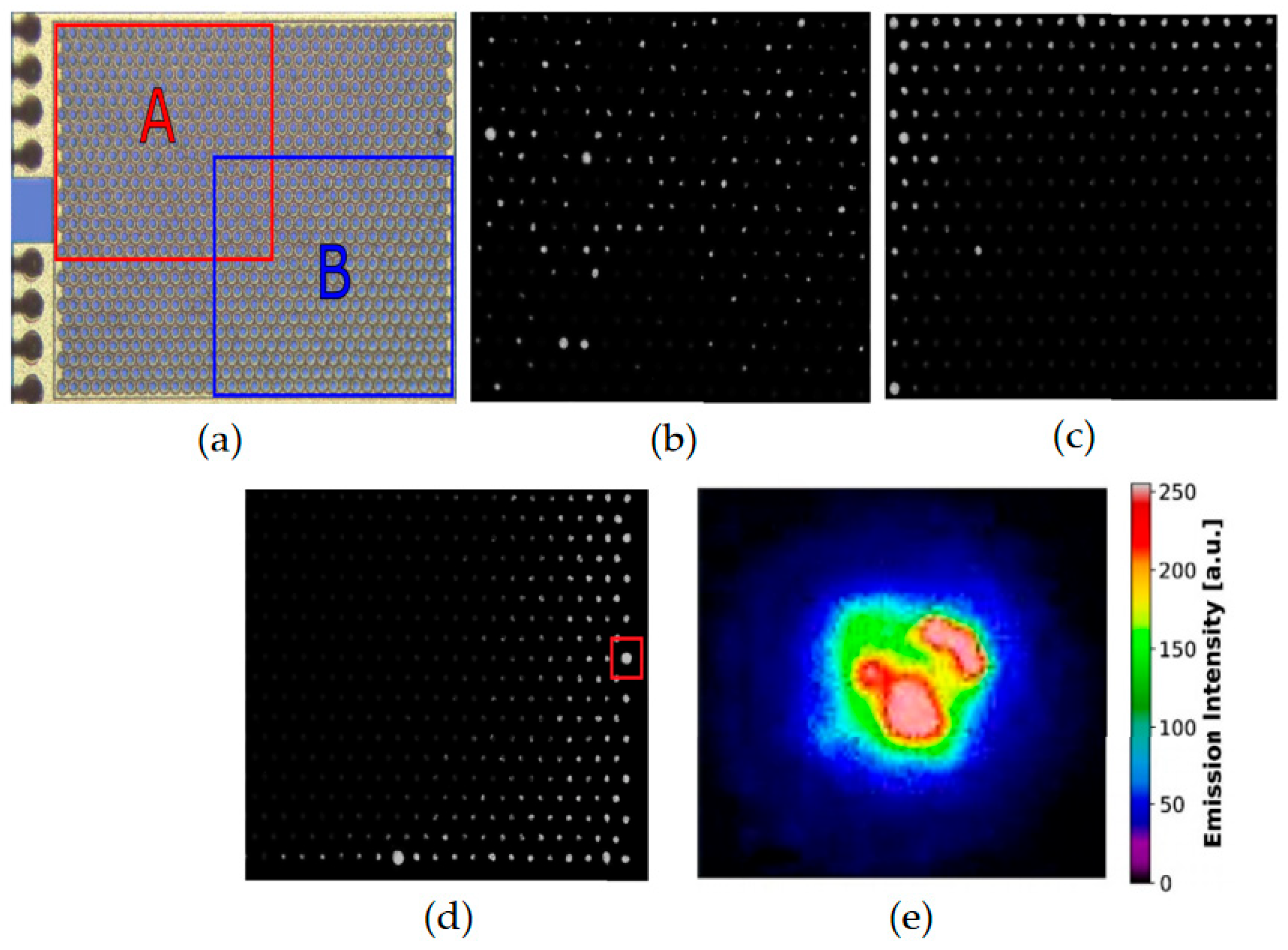
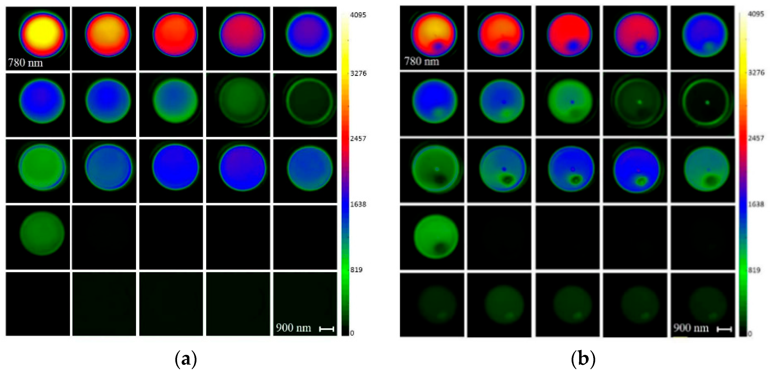
4.5. µ-PL Mapping
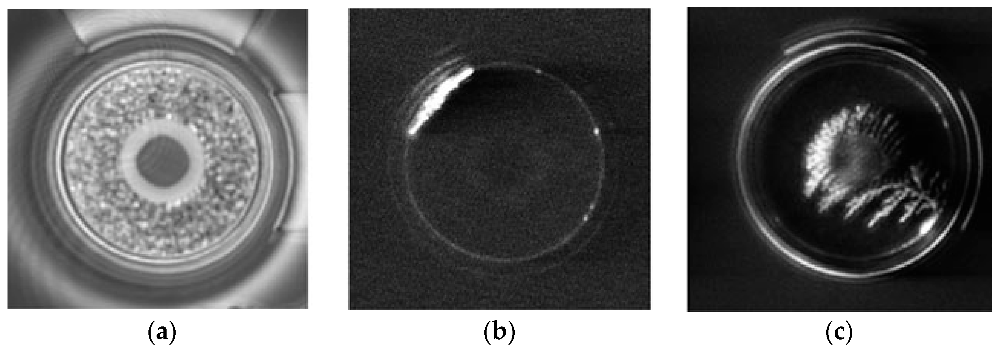
4.6. EMMI
4.7. CL
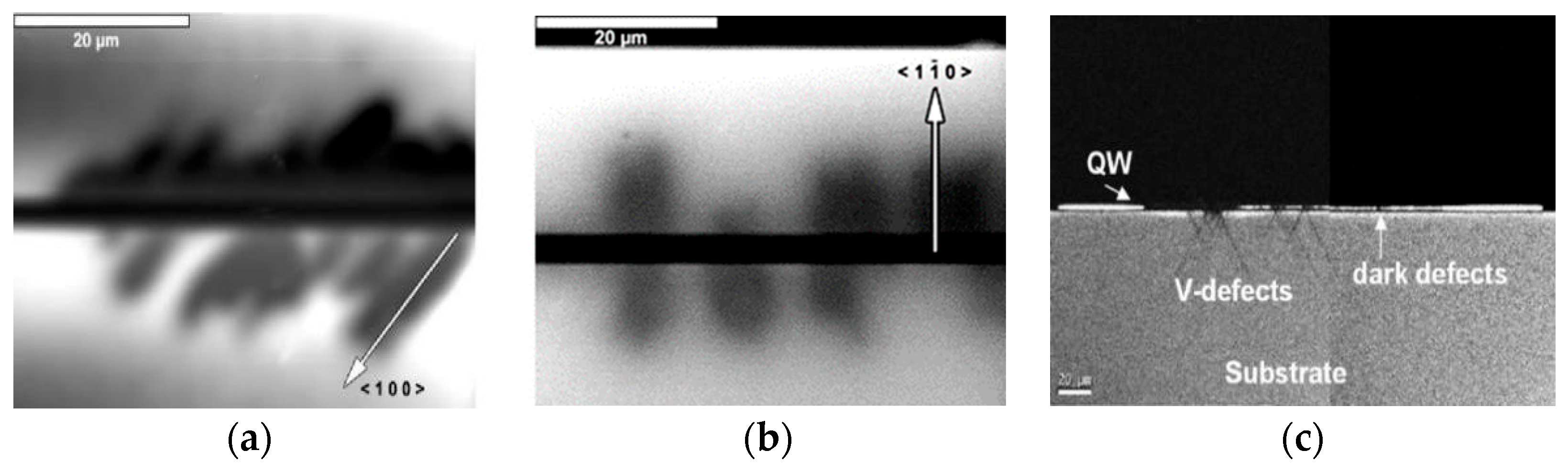
4.8. TEM
4.9. ECCI
4.10. Raman
5. Failure Improvement Measures
5.1. Preparation Process
5.2. Reliability Screening
5.2.1. High-Temperature Storage
5.2.2. High- and Low-Temperature Shock
5.2.3. High-Temperature Power Aging
5.3. Method Application
6. Conclusions
Author Contributions
Funding
Data Availability Statement
Acknowledgments
Conflicts of Interest
References
- Epperlein, P.W. Semiconductor Laser Engineering, Reliability and Diagnostics: Basic Diode Laser Engineering Principles; John Wiley & Sons Ltd.: Hoboken, NJ, USA, 2013; pp. 35–39, 72–74, 326–332. [Google Scholar]
- Cooper, D.P.; Gooch, C.H.; Sherwell, R.J. Internal self-damage of gallium arsenide lasers. IEEE J. Quantum Electron. 1966, 2, 329–330. [Google Scholar] [CrossRef]
- Kressel, H.; Mierop, H. Catastrophic Degradation in GaAs Injection Lasers. J. Appl. Phys. 1968, 38, 5419–5421. [Google Scholar] [CrossRef]
- Orton, J.W. Reliability and Degradation of Semiconductor Lasers and LEDs. Opt. Acta Int. J. Opt. 1992, 39, 1799–1800. [Google Scholar] [CrossRef]
- Ueda, O. On Degradation Studies of III–V Compound Semiconductor Optical Devices over Three Decades: Focusing on Gradual Degradation. Jpn. J. Appl. Phys. 2010, 49, 090001–090008. [Google Scholar] [CrossRef] [Green Version]
- Ueda, O. Reliability and Degradation of III-V Optical Devices. In Materials and Reliability Handbook for Semiconductor Optical and Electron Devices; Springer: New York, NY, USA, 2013; pp. 87–120. [Google Scholar]
- Epperlein, P.W.; Buchmann, P.; Jakubowicz, A. Lattice disorder, facet heating and catastrophic optical mirror damage of AlGaAs quantum well lasers. Appl. Phys. Lett. 1993, 62, 455–457. [Google Scholar] [CrossRef]
- Jakubowicz, A.; Oosenbrug, A.; Forster, T. Laser operation-induced migration of beryllium at mirrors of GaAs/AlGaAs laser diodes. Appl. Phys. Lett. 1993, 63, 1185–1187. [Google Scholar] [CrossRef]
- Jakubowicz, A.; Oosenbrug, A. SEM/EBIC characterization of degradation at mirrors of GaAs/AlGaAs laser diodes. Microelectron. Eng. 1994, 24, 189–194. [Google Scholar] [CrossRef]
- Ichikawa, H.; Kumagai, A.; Kono, N.; Matsukawa, S.; Fukuda, C.; Iwai, K.; Ikoma, N. Dependence of facet stress on reliability of AlGaInAs edge-emitting lasers. J. Appl. Phys. 2010, 107, 083109. [Google Scholar] [CrossRef]
- Krueger, J.; Sabharwal, R.; Mchugo, S.; Nguyen, K.; Tan, N.; Janda, N.; Mayonte, M.; Heidecker, M.; Eastley, D.; Keever, M.; et al. Studies of ESD-related failure patterns of Agilent oxide VCSELs. Proc. SPIE 2003, 4994, 162–172. [Google Scholar]
- Sin, Y.; Ives, N.; Lalumondiere, S.; Presser, N.; Moss, S.C. Catastrophic optical bulk damage (COBD) in high power multi-mode InGaAs-AlGaAs strained quantum well lasers. Proc. SPIE 2011, 7918, 791803-1–791803-11. [Google Scholar]
- Pitts, O.J.; Benyon, W.; Springthorpe, A.J. Modeling and process control of MOCVD growth of InAlGaAs MQW structures on InP. J. Cryst. Growth 2014, 393, 81–84. [Google Scholar] [CrossRef]
- Chu, S.; Nakahara, S.; Twigg, M.E.; Koszi, L.; Flynn, E.; Chin, A.; Segner, B.; Johnston, W. Defect mechanisms in degradation of 1.3-μm wavelength channeled-substrate buried heterostructure lasers. J. Appl. Phys. 1988, 63, 611–623. [Google Scholar] [CrossRef]
- Jianping, J. Semiconductor Laser, 1st ed.; Publishing House of Electronics Industry: Beijing, China, 2000; pp. 330–331. [Google Scholar]
- Jiménez, J. Laser diode reliability: Crystal defects and degradation modes. Comptes Rendus Phys. 2003, 4, 663–673. [Google Scholar] [CrossRef]
- Tomiya, S.; Goto, O.; Ikeda, M. Structural Defects and Degradation Phenomena in High-Power Pure-Blue InGaN-Based Laser Diodes. Proc. IEEE 2010, 98, 1208–1213. [Google Scholar] [CrossRef]
- Hortelano, V.; Anaya, J.; Souto, J.; Jimenez, J.; Perinet, J.; Laruelle, F. Defect signatures in degraded high power laser diodes. Microelectron. Reliab. 2013, 53, 1501–1505. [Google Scholar] [CrossRef]
- Ueda, O.; Umebu, I.; Yamakoshi, S.; Kotani, T. Nature of dark defects revealed in InGaAsP/InP double heterostructure light emitting diodes aged at room temperature. J. Appl. Phys. 1982, 53, 2991–2997. [Google Scholar] [CrossRef]
- Shi, B.; Pinna, S.; Zhao, H.; Zhu, S.; Klamkin, J. Lasing Characteristics and Reliability of 1550 nm Laser Diodes Monolithically Grown on Silicon. Phys. Status Solidi (A) 2021, 218, 2000374. [Google Scholar] [CrossRef]
- Ahrens, R.G.; Jaques, J.J.; Piccirilli, A.B.; Camarda, R.M.; Fields, A.B.; Lawrence, K.R.; Dutta, N.K.; Luvalle, M.J. Failure mode analysis of high-power laser diodes. Proc. SPIE 2002, 4648, 30–42. [Google Scholar]
- Epperlein, P.W. Semiconductor Laser Engineering, Reliability and Diagnostics: A Practical Approach to High Power and Single Mode Devices; John Wiley & Sons Ltd.: Hoboken, NJ, USA, 2013; pp. 229–231. [Google Scholar]
- Shi, J.W. Semiconductor laser degradation and its screening. Semicond. Optoelectron. 1997, 1, 14–19. [Google Scholar]
- Fukuda, M. Historical overview and future of optoelectronics reliability for optical fiber communication systems. Microelectron. Reliab. 2000, 40, 27–35. [Google Scholar] [CrossRef]
- Ueda, O. Reliability issues in III–V compound semiconductor devices: Optical devices and GaAs-based HBTs. Microelectron. Reliab. 1999, 39, 1839–1855. [Google Scholar] [CrossRef]
- Liu, Q.K.; Kong, J.X.; Zhu, L.N.; Xiong, C.; Ma, X.Y. Failure Mode Analysis of High-power Laser Diodes by Electroluminescence. Chin. J. Lumin. 2018, 39, 180–187. [Google Scholar]
- Fukuda, M.; Mura, G. Laser Diode Reliability. Adv. Laser Diode Reliab. 2021, 1–49. [Google Scholar] [CrossRef]
- Tomm, J.W.; Ziegler, M.; Hempel, M.; Elsaesser, T. Mechanisms and fast kinetics of the catastrophic optical damage (COD) in GaAs-based diode lasers. Laser Photonics Rev. 2011, 5, 422–441. [Google Scholar] [CrossRef]
- Yoo, J.S.; Lee, H.H.; Zory, P. Temperature rise at mirror facet of CW semiconductor lasers. Quantum Electron. IEEE J. Quantum Electron. 1992, 28, 635–639. [Google Scholar] [CrossRef]
- Chuang, T.H.; Lin, H.J.; Wang, H.C.; Chuang, C.H.; Tsai, C.H. Mechanism of Electromigration in Ag-Alloy Bonding Wires with Different Pd and Au Content. J. Electron. Mater. 2014, 44, 623–629. [Google Scholar] [CrossRef]
- Korhonen, M.A.; Bo/Rgesen, P.; Tu, K.N.; Li, C.Y. Stress evolution due to electromigration in confined metal lines. J. Appl. Phys. 1993, 73, 3790–3799. [Google Scholar] [CrossRef]
- Tomm, J.W.; Tien, T.Q.; Oudart, M.; Nagle, J. Aging properties of high-power diode laser arrays: Relaxation of packaging-induced strains and corresponding defect creation scenarios. In Proceedings of the Cleo/Europe Conference on Lasers and Electro-optics Europe, Munich, Germany, 12–17 June 2005; IEEE: Piscataway Township, NJ, USA, 2005; p. 112. [Google Scholar]
- Okada, H.; Nakanishi, Y.; Wakahara, A.; Yoshida, A.; Ohshima, T. 380 keV proton irradiation effects on photoluminescence of Eu-doped GaN. Nucl. Instrum. Methods Phys. Research. B Beam Interact. Mater. At. 2008, 266, 853–856. [Google Scholar] [CrossRef]
- O’Neill, J.; Ross, I.M.; Cullis, A.G.; Wang, T.; Parbrook, P.J. Electron-beam-induced segregation in InGaN/GaN multiple-quantum wells. Appl. Phys. Lett. 2003, 83, 1965–1967. [Google Scholar] [CrossRef]
- Yamaguchi; Masafumi; Okuda; Takeshi. Minority-carrier injection-enhanced annealing of radiation damage to InGaP solar cells. Appl. Phys. Lett. 1997, 70, 2180–2182. [CrossRef]
- Neitzert, H.C.; Piccirillo, A.; Gobbi, B. Sensitivity of proton implanted VCSELs to electrostatic discharge pulses. IEEE J. Sel. Top. Quantum Electron. 2002, 7, 231–241. [Google Scholar] [CrossRef]
- Mchugo, S.A.; Krishnan, A.; Krueger, J.J.; Yong, L.; Tan, N.; Osentowski, T.; Xie, S.; Mayonte, M.S.; Herrick, R.W.; Deng, Q. Characterization of failure mechanisms for oxide VCSELs. Proc. SPIE—Int. Soc. Opt. Eng. 2003, 4994, 55–66. [Google Scholar]
- Mendizabal, L.; Verdier, F.; Deshayes, Y.; Ousten, Y.; Danto, Y.; Béchou, L. Reliability of Laser Diodes for High-rate Optical Communications—A Monte Carlo-based Method to Predict Lifetime Distributions and Failure Rates in Operating Conditions. In Advanced Laser Diode Reliability; Elsevier: Amsterdam, The Netherlands, 2021; pp. 79–137. [Google Scholar]
- Mao, S.S. Acceleration model for accelerated life test. Qual. Reliab. 2003, 02, 15–17. [Google Scholar]
- Jennifer, L.K.; Joel, G.K. Erroneous Arrhenius: Modified Arrhenius Model Best Explains the Temperature Dependence of Ectotherm Fitness. Am. Nat. 2010, 176, 227–233. [Google Scholar]
- Kececioglu, D.; Jacks, J.A. The Arrhenius, Eyring, inverse power law and combination models in accelerated life testing. Reliab. Eng. 1984, 8, 1–9. [Google Scholar] [CrossRef]
- Hakamipour, N. Comparison between constant-stress and step-stress accelerated life tests under a cost constraint for progressive type I censoring. Seq. Anal. 2021, 40, 17–31. [Google Scholar] [CrossRef]
- Moser, A.; Latta, E.E. Arrhenius parameters for the rate process leading to catastrophic damage of AlGaAs-GaAs laser facets. J. Appl. Phys. 1992, 71, 4848–4853. [Google Scholar] [CrossRef]
- Oosenbrug, A.; Latta, E.E. High-power operational stability of 980 nm pump lasers for EDFA applications. Lasers Electro-Opt. Soc. Meet. 1994, 2, 37–38. [Google Scholar]
- Amzajerdian, F.; Meadows, B.L.; Ba Ker, N.R.; Ba Ggott, R.S.; Singh, U.N.; Kavaya, M.J. Advancement of High Power Quasi-CW Laser Diode Arrays For Space-based Laser Instruments. In Proceedings of the SPIE’s Fourth International Asia-Pacific Environmental Remote Sensing Symposium, Honolulu, HI, USA, 8–12 November 2004; SPIE: Washington, DC, USA, 2005; Volume 5659. [Google Scholar]
- Stephen, M.; Krainak, M.; Dallas, J. Quasi-cw Laser Diode Bar Life Tests. In Proceedings of the SPIE—Laser-Induced Damage in Optical Materials; SPIE: Washington, DC, USA, 1997; Volume 3244. [Google Scholar]
- Fouksman, M.; Lehconen, S.; Haapamaa, J.; Kennedy, K.; Li, J. High-performance high-reliability 880-nm diode laser bars and fiber-array packages. Proc. SPIE 2006, 6104, 61040A-1–61040A-6. [Google Scholar]
- Bonati, G. Exploring failure probability of high-power laser diodes. Photonics Spectra 2003, 37, 56–58. [Google Scholar]
- Lu, G.G.; To, G.T.; Yao, S.; Shan, X.N.; Sun, Y.F.; Liu, Y.; Wang, L.J. Reliability study of high-power semiconductor lasers. Laser J. 2005, 4, 14–15. [Google Scholar]
- Wang, D.H.; Li, Y.J.; An, Z.F. Study on step-accelerated aging of high-power semiconductor lasers. Micro-Nanoelectron. 2008, 9, 508–511. [Google Scholar]
- Bao, L. Reliability of high performance 9xx-nm single emitter laser diodes. Proc. SPIE-Int. Soc. Opt. Photonics 2010, 7583, 758302-1–758302-10. [Google Scholar]
- Bao, L.; Leisher, P.; Wang, J.; Devito, M.; Xu, D.; Grimshaw, M.; Dong, W.; Guan, X.; Zhang, S.; Bai, C. High reliability and high performance of 9xx-nm single emitter laser diodes. Proc. SPIE—Int. Soc. Opt. Eng. 2011, 7918, 791806. [Google Scholar]
- Sin, Y.; Lingley, Z.; Brodie, M.; Presser, N.; Moss, S.C. Catastrophic optical bulk degradation (COBD) in high-power single- and multi-mode InGaAs-AlGaAs strained quantum well lasers. IEEE J. Sel. Top. Quantum Electron. 2017, 23, 1500813. [Google Scholar] [CrossRef]
- Sin, Y.; Presser, N.; Lingley, Z.; Brodie, M.; Moss, S.C. Reliability, failure modes, and degradation mechanisms in high power single- and multi-mode InGaAs-AlGaAs strained quantum well lasers. Proc. SPIE—Int. Soc. Opt. Eng. 2016, 9733, 973304. [Google Scholar]
- Wang, W.C.; Ji, H.Q.; Qi, Q.; Wang, C.L.; Ni, Y.X.; Liu, S.P.; Ma, S. Reliability study and failure analysis of high-power semiconductor lasers. J. Lumin. 2017, 38, 165–169. [Google Scholar]
- Nie, Z.Q.; Wang, M.P.; Sun, Y.B.; Li, S.N.; Wu, D. Thermally accelerated lifetime test of conduction-cooled high-power semiconductor laser single-bar devices in CW operation mode. J. Emit. Light 2019, 40, 1136–1145. [Google Scholar]
- Vanzi, M.; Salmini, G.; Palo, R.D. New FIB/TEM evidence for a REDR mechanism in sudden failures of 980 nm SL SQW InGaAs/AlGaAs pump laser diodes. Microelectron. Reliab. 2000, 40, 1753–1757. [Google Scholar] [CrossRef]
- Akamatsu, B. Electron beam-induced current in direct band-gap semiconductors. J. Appl. Phys. 1981, 52, 7245–7250. [Google Scholar] [CrossRef]
- Henoc, P.; Benetton-Martins, R.; Akamatsu, B. Ebic and CL Study of Laser Degradation. J. De Phys. IV 1991, 1, C6-317–C6-322. [Google Scholar] [CrossRef]
- Boudjani, A.; Sieber, B.; Cleton, F.; Rudra, A. Cl and EBIC analysis of a p + −InGaAs/n-InGaAs/n-InP/n + −InP heterostructure. Mater. Sci. Eng. B 1996, 42, 192–198. [Google Scholar] [CrossRef]
- Sin, Y.; Ayvazian, T.; Brodie, M.; Lingley, Z. Catastrophic optical bulk degradation in high-power single- and multi-mode InGaAs-AlGaAs strained QW lasers: Part II. Proc. SPIE 2018, 10514, 10514-1–10514-14. [Google Scholar]
- Xiu, H.; Xu, P.; Wen, P.; Zhang, Y.; Yang, J. Rapid degradation of InGaN/GaN green laser diodes. Superlattices Microstruct. 2020, 142, 106517. [Google Scholar] [CrossRef]
- Takeshita, T.; Iga, R.; Yamamoto, M.; Sugo, M. Analysis of interior degradation of a laser waveguide using an OBIC monitor. Microelectron. Reliab. 2007, 47, 2135–2140. [Google Scholar] [CrossRef]
- Hsu, C.L.; Das, S.; Wu, Y.S.; Kao, F.J. Spectrally resolved optical beam inducedcurrent imaging of ESD induced defects on VCSELs. OSA Contin. 2021, 4, 711–719. [Google Scholar] [CrossRef]
- Cole, E.I., Jr.; Tangyunyong, P.; Benson, D.A.; Barton, D.L. TIVA and SEI developments for enhanced front and backside interconnection failure analysis. Microelectron. Reliab. 1999, 39, 991–996. [Google Scholar] [CrossRef]
- Reissner, M. Fault localization at high voltage devices using thermally induced voltage alteration (TIVA). Microelectron. Reliab. 2007, 47, 1561–1564. [Google Scholar] [CrossRef]
- Herrick, R.W. Reliability and degradation of vertical-cavity surface-emitting lasers. In Materials and Reliability Handbook for Semiconductor Optical and Electron Devices; Ueda, O., Pearton, S.J., Eds.; Springer: New York, NY, USA, 2013; pp. 195–197. [Google Scholar]
- Yongkun, S.; Zachary, L.; Talin, A.; Miles, B.; Neil, I. Catastrophic Optical Bulk Damage—A New Failure Mode in High-Power InGaAs-AlGaAs Strained Quantum Well Lasers. Mrs Adv. 2018, 3, 3329–3345. [Google Scholar]
- Sanayeh, M.B.; Jaeger, A.; Schmid, W.; Tautz, S.; Brick, P.; Streubel, K.; Bacher, G. Investigation of dark line defects induced by catastrophic optical damage in broad-area AlGaInP laser diodes. Appl. Phys. Lett. 2006, 89, 10111. [Google Scholar] [CrossRef]
- Fabbro, R.; Haber, T.; Fasching, G.; Coppeta, R.; Michael, P.; Werner, G. Defect localization in high-power vertical cavity surface emitting laser arrays by means of reverse biased emission microscopy. Meas. Sci. Technol. 2021, 32, 095406. [Google Scholar] [CrossRef]
- Peng, J.; Li, Q.; Xing, Z.; Zhang, J.; Ning, Y.Q. Reliability Study of Grating Coupled Semiconductor Laser Based on Raman Spectra Technique. Spectrosc. Spectr. Anal. 2016, 36, 1745–1748. [Google Scholar]
- Yamasaki, K.; Yoshida, M.; Sugano, T. Deep Level Transient Spectroscopy of Bulk Traps and Interface States in Si MOS Diodes. Jpn. J. Appl. Phys. 1979, 18, 113–122. [Google Scholar] [CrossRef]
- Shin, Y.C.; Dong, H.; Kang, J.; Chang, Y.K.; Kim, T.G. Optimization of 660-nm-Band AlGaInP Laser Diodes by Using Deep-Level Transient Spectroscopy Analyses. J. Korean Phys. Soc. 2007, 50, 866–870. [Google Scholar] [CrossRef]
- Evtikhiev, V.P.; Kotel’Nikov, E.; Kudryashov, I.V.; Tokranov, V.E.; Faleev, N.N. Correlation between the reliability of laser diodes and the crystal perfection of epitaxial layers estimated by high-resolution x-ray diffractometry. Semiconductors 1999, 33, 590–593. [Google Scholar] [CrossRef]
- Qiao, Y.B.; Feng, S.W.; Xiong, C.; Wang, X. Spatial hole burning degradation of AlGaAs/GaAs laser diodes. Appl. Phys. Lett. 2011, 99, 103506. [Google Scholar] [CrossRef] [Green Version]
- Fernández-Caballero, A. A Review on Machine and Deep Learning for Semiconductor Defect Classification in Scanning Electron Microscope Images. Appl. Sci. 2021, 11, 9508. [Google Scholar]
- Shin, Y.C.; Kim, B.J.; Dong, H.K.; Kim, Y.M.; Kim, T.G. Investigation of Zn diffusion by SIMS and its effects on the performance of AlGaInP-based red lasers. Semicond. Sci. Technol. 2005, 21, 35. [Google Scholar] [CrossRef] [Green Version]
- Zhou, Q.; Li, J.Y.; Liang, H.D.; Wu, C.P. Recent developments on secondary ion mass spectroscopy. J. Chin. Mass Spectrom. Soc. 2004, 25, 113–120. [Google Scholar]
- Yamamoto, S.; Matsuda, I. Time-Resolved Soft X-ray Photoelectron Spectroscopy: Real-Time Observation of Photo-Excited Carriers at Semiconductor Surfaces. Hyomen Kagaku 2016, 37, 9–13. [Google Scholar] [CrossRef] [Green Version]
- Xie, J.; Xu, C.; Huang, W.; Chen, G. An infrared thermal image processing framework based on superpixel algorithm to detect cracks on metal surface. Infrared Phys. Technol. 2014, 67, 266–272. [Google Scholar]
- Kuo, W.; Yue, K. Facing the headaches of early failures: A state-of-the-art review of burn-in decisions. Proc. IEEE 1983, 71, 1257–1266. [Google Scholar] [CrossRef]
- Guijun, H.; Jiawei, S.; Yinbing, G.; Xiaosong, Y.; Jing, L. Noise as reliability screening for semiconductor lasers. Appl. Phys. B 2003, 76, 359–363. [Google Scholar] [CrossRef]
- Zhang, L.P. The Screening Method for Early Failure of Semiconductor Devices. Manag. Technol. SME 2021, 9, 137, 138, 141. [Google Scholar]
- Lee, J.M.; Min, B.G.; Ju, C.W.; Ahn, H.K.; Lim, J.W. High temperature storage test and its effect on the thermal stability and electrical characteristics of AlGaN/GaN high electron mobility transistors. Curr. Appl. Phys. 2016, 17, 157–161. [Google Scholar] [CrossRef]


| Lasing Wavelength | Semiconductor Lasers | Defect Types | Mechanism |
|---|---|---|---|
| 440–450 nm | InGaN/GaN QW lasers | <11-20> a-type dislocations [17] | Climb mechanism involving point defect |
| 808 nm | AlGaAs/GaAs QW-SCH lasers | <110> DLDs Dislocations dipoles [18] | Gliding mechanism |
| 980 nm | InGaAs/AlGaAs QW lasers | <100> DLDs Dislocation dipoles or climbed dipoles [18] | Climb mechanism involving point defect |
| <1-10> DLDs Edge dislocation dipoles | Gliding mechanism not involving point defect | ||
| 1300 nm | InGaAsP/InP QW lasers | <100> DLDs Dislocation dipoles [19] | Climb mechanism involving point defect |
| 1550 nm | InGaAs/InP QW lasers | V-shaped defects DLDs Misfit dislocations [20] | Climb mechanism |
| Method | Detection category | Selectivity | Advantages | Limitation |
|---|---|---|---|---|
| EBIC | Non-destructive (VCSEL, topside) Non-destructive (EEL, topside and front facet) Destructive (EEL, backside) | High | Detecting the DLDs, stacking faults and precipitates in the active region nearby | Defects in cladding or contact layer are not visible |
| OBIC | Non-destructive (VCSEL, topside) Non-destructive (EEL, topside and front facet) Destructive (EEL, backside) | High | Detecting degradation area and degree in the buried heterojunction and waveguide layers | For high-speed devices, the ability to observe the spectral response adequately is limited |
| TIVA | Non-destructive (VCSEL, topside) Non-destructive (EEL, topside) | High | Sensitive to leakage current and can detect the failure both on the surface and below | Signal might be blocked by metallic layers |
| EL | Non-destructive (VCSEL, topside) Non-destructive (EEL, topside and front facet) Destructive (EEL, backside) | Medium | Good at detecting the development of DLDs caused by luminescence-killing dislocation networks in the laser cavity | Not suited to detecting lasers with blanket metal over the epi-side, or mounted epi-side-down |
| µ-PL | Non-destructive (epitaxial wafer, topside) Non-destructive (VCSEL, topside) Non-destructive (EEL, topside) Destructive (EEL, backside) | High | Measures isolated defects and residual mechanical stress induced by the packaging process | Cannot provide information of luminescence features with dimensions below the classical diffraction limit |
| CL | Non-destructive (epitaxial wafer, topside) Non-destructive (VCSEL, topside) Non-destructive (EEL, topside) Destructive (EEL, backside) | High | Sensitive to the presence of non-recombination centers, high lateral and in-depth resolution | Result depends greatly on the device resistances |
| EMMI | Non-destructive (VCSEL, topside) Non-destructive (EEL, topside and front facet) | Medium | The luminescent defects can be located, low leakage current requirement | Poor resolution of non-luminous defects in metallic shaded areas |
| DLTS | Non-destructive (VCSEL, topside) Non-destructive (EEL, topside) | High | Sensitive to deep level defects, comprehensive characterization information | Cannot obtain deep energy level electron wave functions or defect internal information |
| Raman | Non-destructive (VCSEL, topside) Non-destructive (EEL, topside) | Medium | No need for sample processing, short time, high sensitivity | Weak signal strength |
| FIB-TEM | Destructive (VCSEL, topside) Destructive (EEL, topside) | High | Maximum magnification, high image quality, deep failure analysis; root cause identification | Significant sample preparation time, small sampling volumes, unable to detect the materials’ instability in high-energy electron beams |
| XRD | Non-destructive (VCSEL, topside) Non-destructive (EEL, topside) | High | Small sample size and simple interpretation result | Susceptible to interference of mutual elements and superposition peaks |
| SEM | Non-destructive (epitaxial wafer, VCSEL, EEL, topside) Non-destructive (epitaxial wafer, cross-section) Non-destructive (EEL, front facet) Destructive (EEL, backside) | High | Detects failures such as delamination, oxidation contamination, and melting at the surface | Cannot detect root cause hidden below surface |
| ECCI | Non-destructive (epitaxial wafer, topside) Non-destructive (VCSEL, topside) Non-destructive (EEL, topside) Destructive (EEL, backside) | High | High precision, no need for sample preparation, allows the examination of large area of specimen | Resolution is limited by SEM system; the background signal is strong; and dislocation detection and signal analysis are prone to interference |
| SIMS | Destructive (epitaxial wafer, VCSEL, EEL, topside) | High | Can acquire the information of several atomic layers or even single elements | Difficulties in quantitative analysis |
| XPS | Non-destructive (VCSEL, topside) Non-destructive (EEL, topside) | High | Good repeatability of spectral line, fast speed and high sensitivity | Low energy resolution and low peak-to-back ratio |
| IRT | Non-destructive (VCSEL, topside) Non-destructive (EEL, front facet) Destructive (EEL, topside) | Medium | Strong signal and easy to measure | Large quantitative analysis errors and low sensitivity |
Publisher’s Note: MDPI stays neutral with regard to jurisdictional claims in published maps and institutional affiliations. |
© 2022 by the authors. Licensee MDPI, Basel, Switzerland. This article is an open access article distributed under the terms and conditions of the Creative Commons Attribution (CC BY) license (https://creativecommons.org/licenses/by/4.0/).
Share and Cite
Song, Y.; Lv, Z.; Bai, J.; Niu, S.; Wu, Z.; Qin, L.; Chen, Y.; Liang, L.; Lei, Y.; Jia, P.; et al. Processes of the Reliability and Degradation Mechanism of High-Power Semiconductor Lasers. Crystals 2022, 12, 765. https://doi.org/10.3390/cryst12060765
Song Y, Lv Z, Bai J, Niu S, Wu Z, Qin L, Chen Y, Liang L, Lei Y, Jia P, et al. Processes of the Reliability and Degradation Mechanism of High-Power Semiconductor Lasers. Crystals. 2022; 12(6):765. https://doi.org/10.3390/cryst12060765
Chicago/Turabian StyleSong, Yue, Zhiyong Lv, Jiaming Bai, Shen Niu, Zibo Wu, Li Qin, Yongyi Chen, Lei Liang, Yuxin Lei, Peng Jia, and et al. 2022. "Processes of the Reliability and Degradation Mechanism of High-Power Semiconductor Lasers" Crystals 12, no. 6: 765. https://doi.org/10.3390/cryst12060765
APA StyleSong, Y., Lv, Z., Bai, J., Niu, S., Wu, Z., Qin, L., Chen, Y., Liang, L., Lei, Y., Jia, P., Shan, X., & Wang, L. (2022). Processes of the Reliability and Degradation Mechanism of High-Power Semiconductor Lasers. Crystals, 12(6), 765. https://doi.org/10.3390/cryst12060765