Abstract
The shortcomings with acceptors in p-type III-nitride semiconductors have resulted in not many efforts being presented on III-nitride based p-channel electronic devices (here, field effect transistors (FETs)). The polarization effects in III-nitride superlattices (SLs) lead to the periodic oscillation of the energy bands, exhibiting enhanced ionization of the deep acceptors (Mg in this study), and hence their use in III-nitride semiconductor-based light-emitting diodes (LEDs) and p-channel FETs is beneficial. This study experimentally demonstrates the presence of acceptor-like traps at the positive polarization interfaces acting as the primary source of holes in Ga-polar p-type uniformly doped (AlGaN/AlN)/GaN SLs with limited Mg doping. The observed concentration of holes exceeding that of the dopants incorporated into the samples during growth can be attributed to the ionization of acceptor-like traps, located at 0.8 eV above the valence band of GaN, at positive polarization interfaces. All samples were grown using the metal organic vapor phase epitaxy (MOVPE) technique, and the materials’ characterization was carried out using X-ray diffraction and Hall effect measurements. The hole concentrations experimentally measured are juxtaposed with the calculated value of hole concentrations from FETIS®, and the measured trends in mobility are explained using the amplitude of separation of the two-dimensional hole gas in the systems from the positive polarization interfaces.
1. Introduction
With the promise of next-generation energy-efficient devices round the corner, heterostructures of III-nitrides (Ga, Al, In, B-nitrides) and their alloys are a leading contender to replace conventional semiconductors in high-power and RF electronics [1,2,3,4,5,6,7,8,9,10], enabling higher efficient operation with higher power density. This is in addition to their already well-known use in state-of-the-art light-emitting diodes (LEDs) and laser diodes (LDs) [11,12,13]. Recent work on this materials’ family has also shown its potential for use in solar cells and thermoelectric generators [14,15], novel spintronic and nuclear detection devices [16], plasmonics [17,18], and quantum computing [19,20]. These applications are a result of some attractive properties of this material system, which include (a) high electron mobility, (b) high thermal stability and breakdown field, (c) wide coverage of the direct bandgap range (0.7 eV through 6.2 eV), and (d) well-developed epitaxial growth techniques [21,22]. While the superior properties of electrons (and the two-dimensional electron gas) have led to numerous studies on n-type III-nitride devices, there are a number of shortcomings of the p-type III-nitride material for electronics, leading to only a handful of investigations on p-type materials [23,24,25,26,27,28]. These challenges include (a) low hole mobility, (b) deep acceptor dopant (~170–200 meV from conduction band edge), and (c) issues with making high-quality ohmic contacts to p-type III-nitrides [29]. However, to tap into the full range of advantages that this material system has to offer, the implementation of high-performance p-type devices using III-nitrides is extremely desirable. Using p-type superlattices (SLs) is valuable for III-nitride optoelectronics and p-channel field effect transistors (pFETs) because the polarization effects create a periodic oscillation of the energy bands, enhancing the ionization of the deep acceptors (Mg in this study) [30]. Therefore, the use of Mg-doped GaN/AlGaN SLs is a method toward achieving high hole concentration and mobility simultaneously, and pFETs developed and fabricated around a GaN/AlGaN SL have demonstrated record electrical performance in the normally off mode (enhancement mode) [28,31].
A recent work proposed the existence of acceptor-like traps at the positive polarization interfaces (PPIs), placed 0.8 eV above the valence band of GaN, in N-polar III-nitride systems [32]. The ionization of this acceptor-like trap level was the main source of holes in systems that had insufficient or no Mg doping in them [33]. This study experimentally demonstrates the proposed presence and the effect of these acceptor traps on both the charge and the mobility of holes in the more conventional Ga-polar uniformly doped p-type (AlGaN/AlN)/GaN superlattices.
2. Materials and Methods
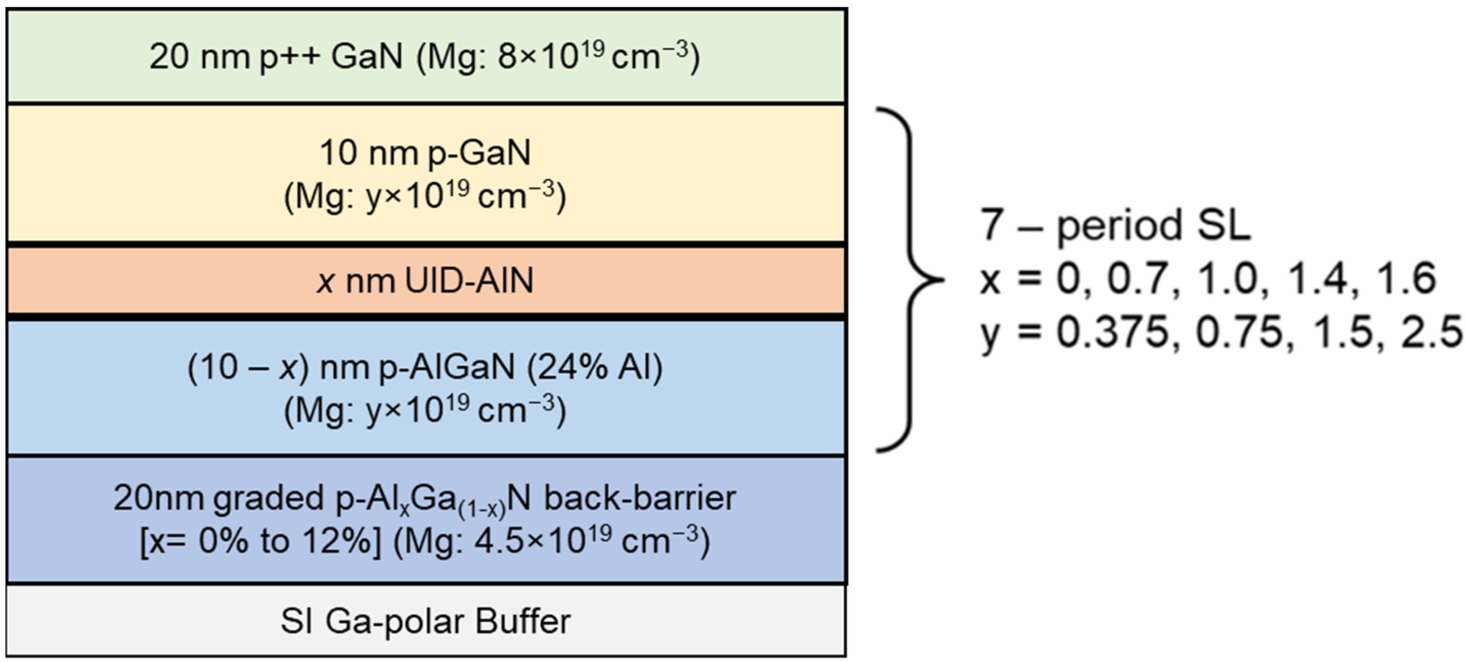
Ga-polar uniformly doped SL samples were grown using the metalorganic vapor phase epitaxy (MOVPE) technique at a temperature of 1155 °C and a pressure of 100 torr on a semi-insulating (SI) GaN buffer layer grown on c-plane sapphire with trimethylgallium (TMGa), trimethylaluminum (TMAl), cyclopentadienyl magnesium (Cp2Mg), and NH3 as precursors. The SL stack growth conditions (temperature and pressure) were the same for both Ga-polar structures reported in this work, and the N-polar structures reported in [32]. Figure 1 shows the p-type uniformly doped Ga-polar (AlGaN/AlN)/GaN SL epitaxial structure. Prior studies have indicated that seven-period SL stacks result in reliable Hall effect measurements, and hence seven-period SL stacks were grown [34]. As shown in Figure 1, each SL period in the stack was 20 nm thick and was composed of (10-x) nm AlGaN:[Mg]/x nm unintentionally doped (u.i.d.) AlN/10 nm GaN:[Mg], where the AlN layer thickness, x, was varied from 0 nm ≤ x ≤ 1.6 nm. In addition, for each AlN thickness, the p-type Mg doping in the AlGaN and GaN was varied as 3.75 × 1018 cm−3 ≤ [Mg] ≤ 2.5 × 1019 cm−3. A 20 nm p++ GaN contact layer, doped with 8 × 1019 cm−3 of Mg, was grown in situ on the SL stack to facilitate fabrication of good contacts to the p-type SL [35]. Before the growth of the SL layers, 20 nm AlxGa(1−x)N:Mg was first grown on the SI buffer, where the composition was graded from x = 0 to 12% to be used as the back barrier for hole transport. From the study in N-polar systems described in Ref. [32], the Al composition in the AlGaN SL layers was chosen to be 24% for this study as it was predicted to have a definitive signature of trap occupancy for the experimental series studied.
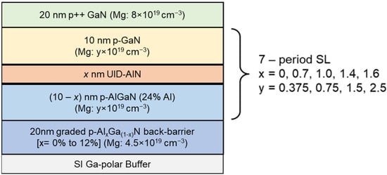
Figure 1.
Structure of SL samples epitaxially grown using MOVPE for this work. The individual SL period had a thickness of 20 nm and was composed of (10 − x) nm p-AlGaN/x nm u.i.d. AlN/10 nm p-GaN, where, x, the AlN layer thickness was 0 nm ≤ x ≤ 1.6 nm. For each of the AlN thickness series samples, the p-type doping (Mg) was varied as 3.75 × 1018 cm−3 ≤ [Mg] ≤ 2.5 × 1019 cm−3. A 20 nm p++ GaN contact layer was also grown in situ to facilitate high-quality contacts.
While the initial study used modulation doped N-polar SL samples grown in the -c or (000-1) direction, this study uses the more widely used Ga-polar orientation for the samples reported. While N-polar orientation allows for modulation doping using MOVPE due to abrupt and sharper Mg doping profiles, Ga-polar orientation faces the problem of Mg diffusion during MOVPE growths [36], and hence uniformly doped samples are presented in this work.
Mg doping in the samples was calibrated using secondary ion mass spectroscopy (SIMS), and the composition and quality of the SL was determined using atomic force microscopy (AFM) and X-ray diffraction (XRD). Figure 2 shows the 2θ-ω XRD spectra for an AlN thickness series with Mg doping = 7.5 × 1018 cm−3, and this also includes an insert with a representative AFM image of an as-grown sample used in the study. As Mg acceptors are passivated in the as-grown epitaxial material, Mg activation was carried out using rapid thermal annealing (RTA) for 3 min at 825 °C and Pd/Au contacts were deposited to prepare the samples for room-temperature Hall measurements (RT-Hall) [27]. Total sheet charge concentration of holes and hole mobility were derived from RT-Hall, and these were compared with calculated values derived from the STR-FETIS® software package.
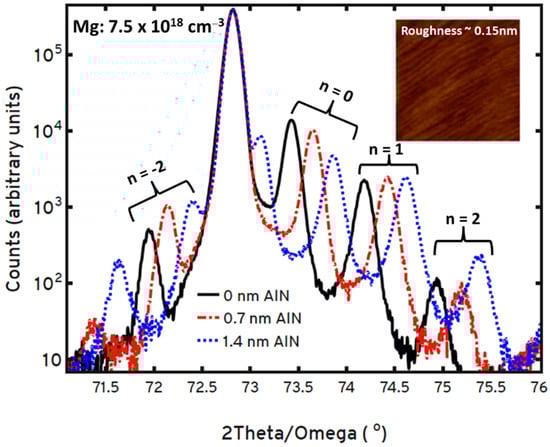
Figure 2.
(2θ-ω) X-ray diffraction spectra for a sample series with varying AlN thickness from 0 nm to 1.6 nm with Mg doping = 7.5 × 1018 cm−3 held constant. Insert: 5 μm × 5 μm atomic force microscopy image with rms roughness = 0.15 nm of a representative sample reported in this work (Mg doping = 7.5 × 1018 cm−3, and AlN thickness in the SL = 1.4 nm).
3. Results
Four-probe Hall effect measurements were carried out at room temperature (RT-Hall), with the magnetic field strengths ranging from −6 T to 6 T, and the total sheet charge measured was compared to the simulated value calculated using STR-FETIS® (STR Japan, Tokyo, Japan). The total hole sheet charge concentration measured for varying AlN layer thicknesses and for the various p-type Mg doping used is shown in Figure 3. The measured hole mobility at room temperature as a function of the AlN layer thickness for the different Mg doping levels presented in this work is shown in Figure 4. The measured hole mobility as a function of the measured total sheet charge for Mg doping levels varying from 3.75 × 1018 cm−3 to 2.5 × 1019 cm−3 is shown in Figure 5. In addition, the figure has samples labeled from A-1 through F-5, corresponding to Table 1.
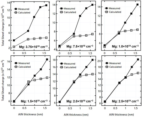
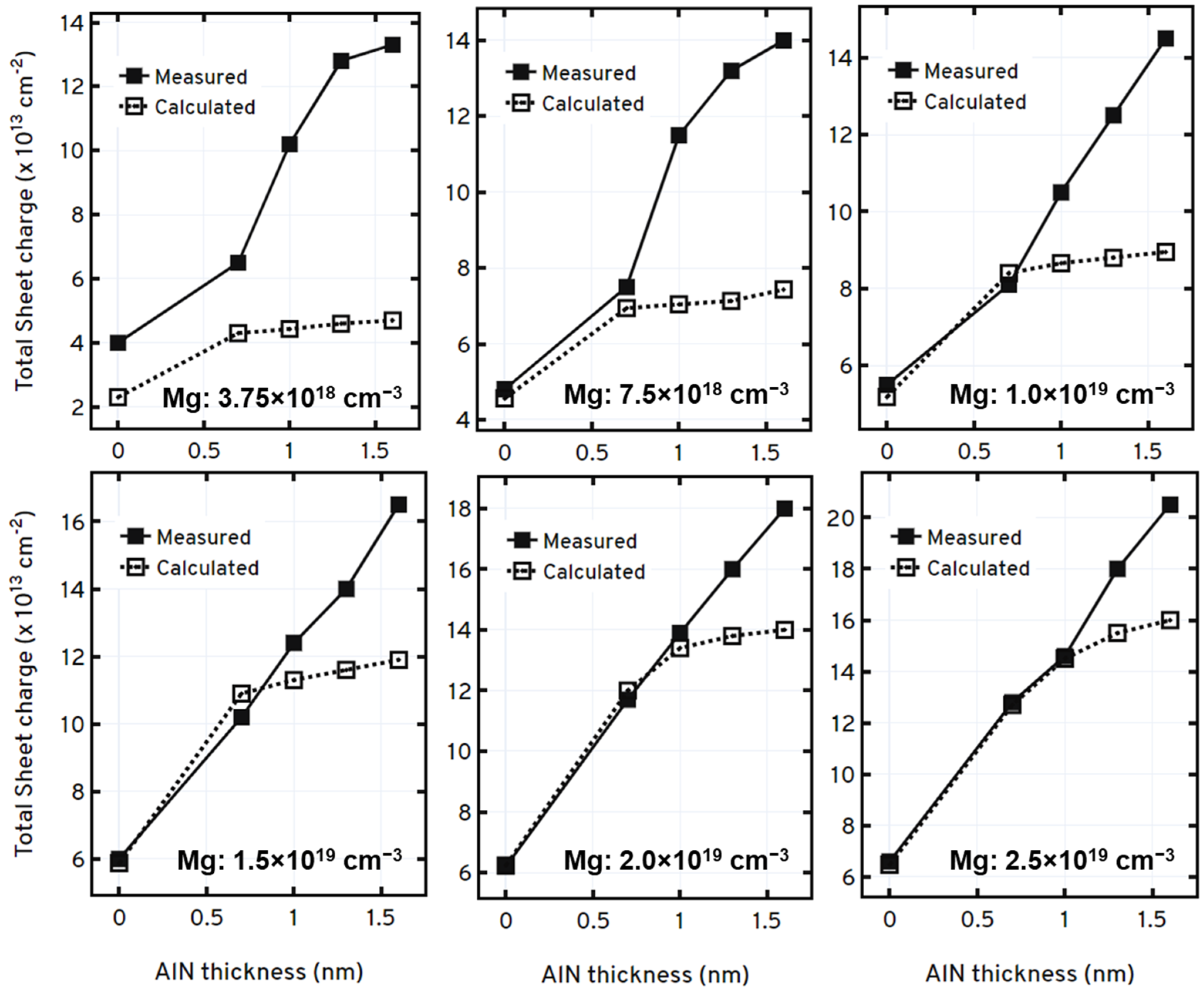
Figure 3.
Results for Hall effect measurements conducted at room temperature on samples presented in this work. The figure shows the total sheet charge concentration of holes measured as the AlN layer thickness is varied for the different Mg doping levels used at each AlN thickness.
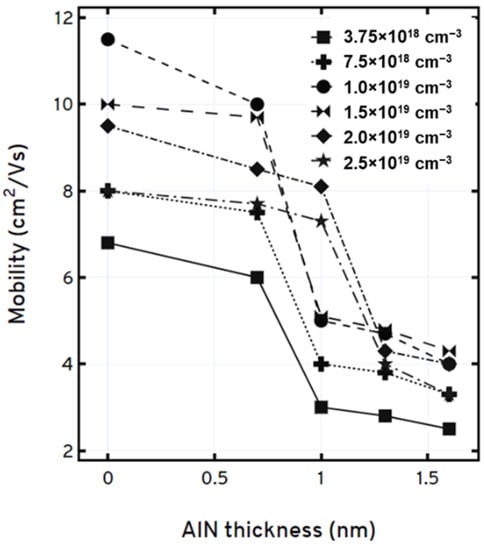
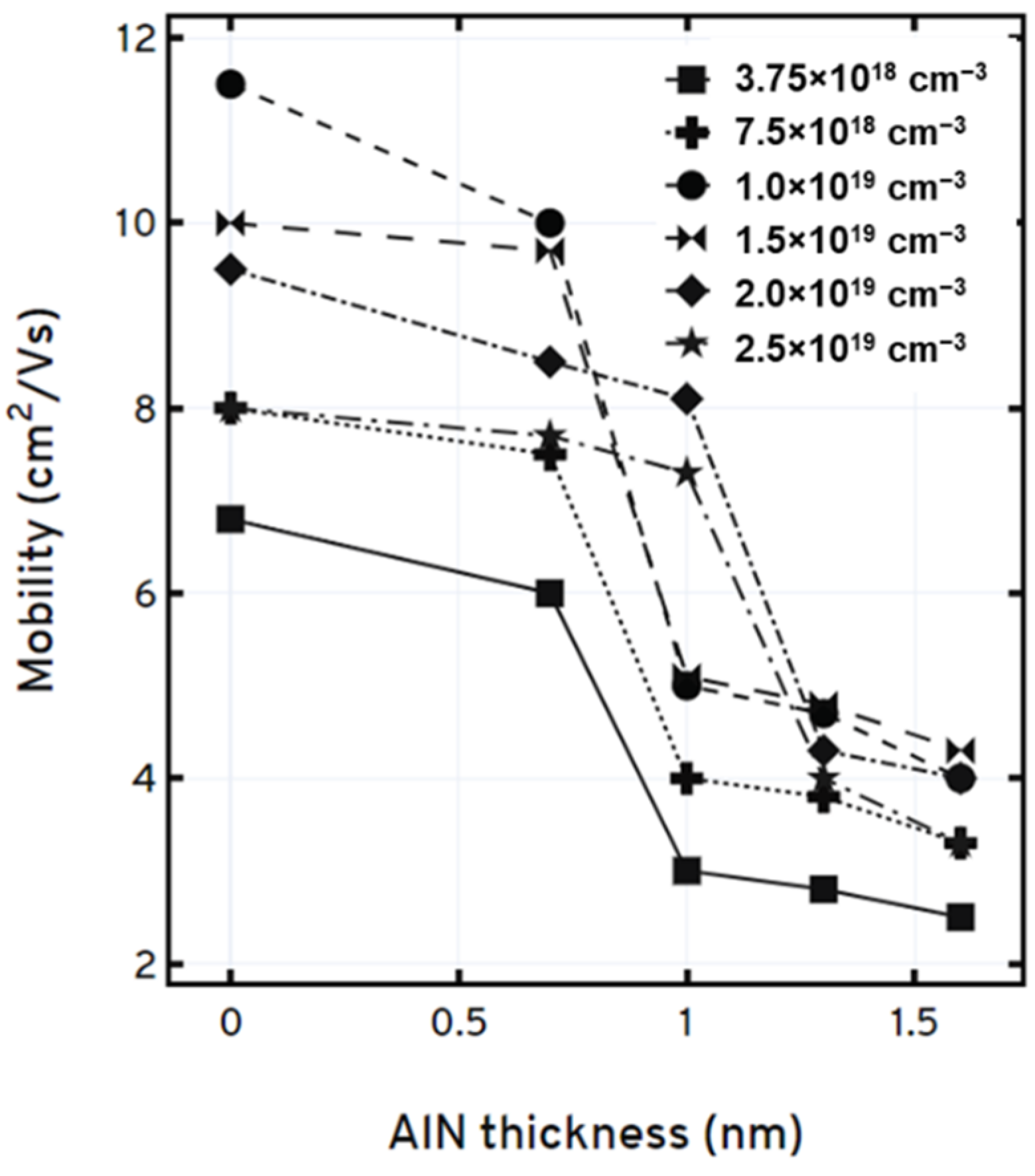
Figure 4.
Room-temperature Hall measurement results for samples presented in this work. This figure shows the measured hole mobility as the AlN layer thickness is varied for the different Mg doping levels used at each AlN thickness.
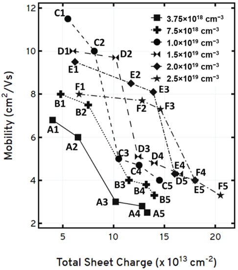
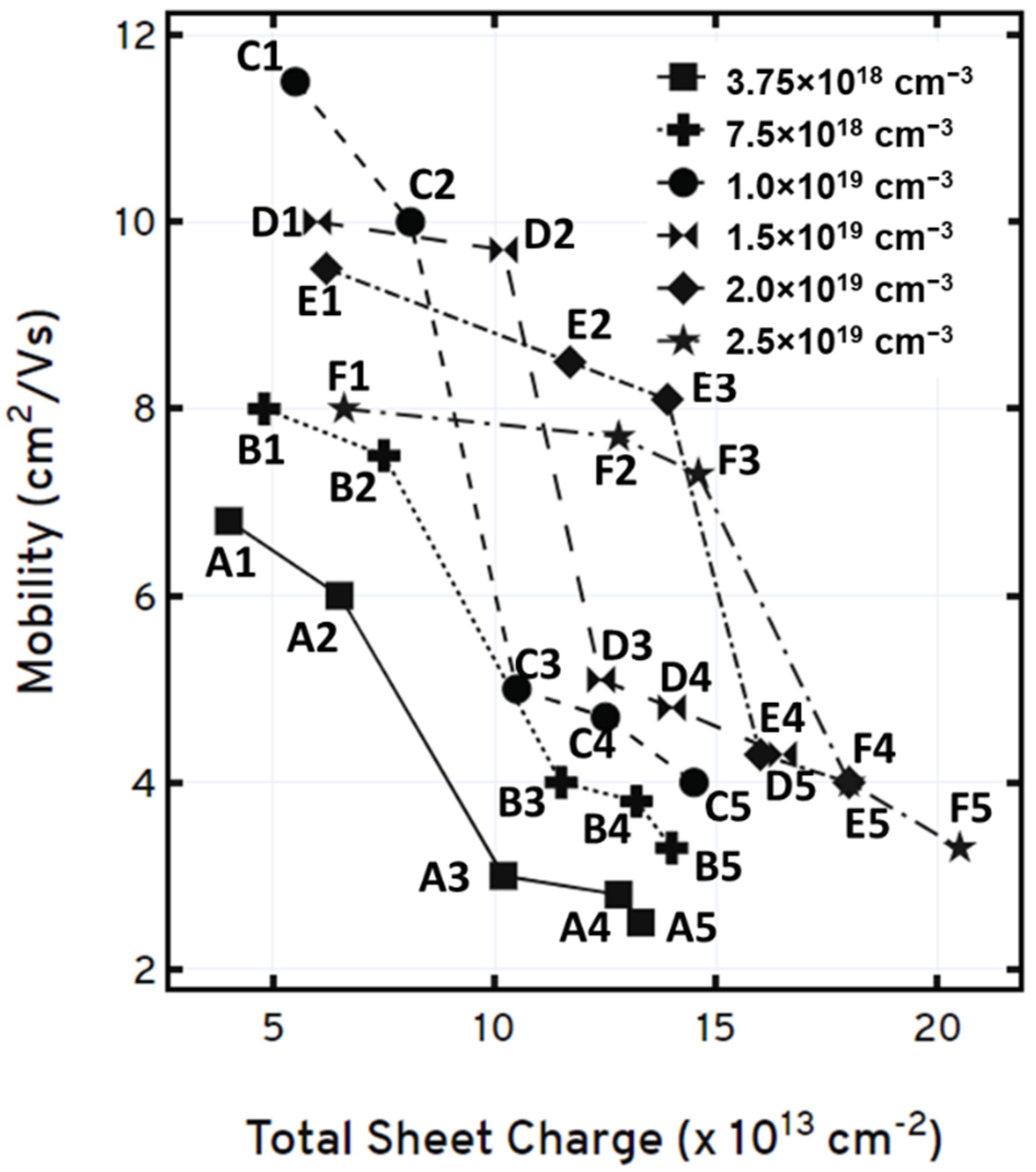
Figure 5.
Room-temperature Hall measurement results for samples reported in this study. The figure shows the measured mobility as a function of the measured total sheet charge concentration for the various Mg doping levels used.

Table 1.
Samples presented in the work labeled A-1 through F-5, with the letter referring to the Mg doping series and the number referring to the AlN thickness series for each doping series. This table also indicates whether the acceptor trap ionization is at interface PPI-1 (AlGaN/AlN interface) or interface PPI-2 (GaN/AlGaN interface) or both interfaces. The table also mentions whether there is an effect on the measured mobility (Δ > 2.0 cm2/Vs) by the ionization of these traps. When traps at both interfaces are unionized, then “-“ is mentioned to indicate that the acceptor-like traps are unionized and therefore have no effect on the mobility (in that case, mobility may be affected slightly by the increase in charge, as indicated in Figure 5).
4. Discussion
Figure 6 shows a cartoon schematic valence band energy diagram of a representative Ga-polar (AlGaN/AlN)/GaN SL structure, without Mg doping, which will be used to explain the trends in the Discussion section going ahead.
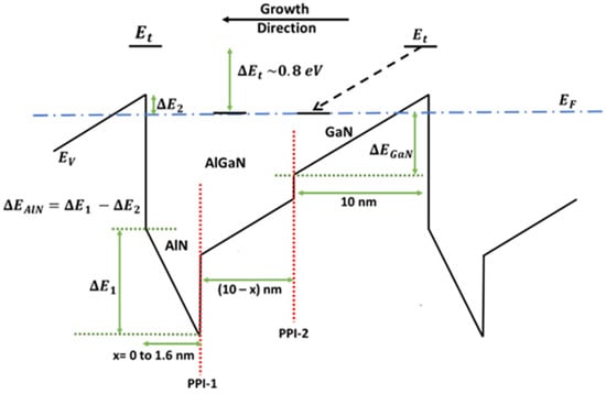
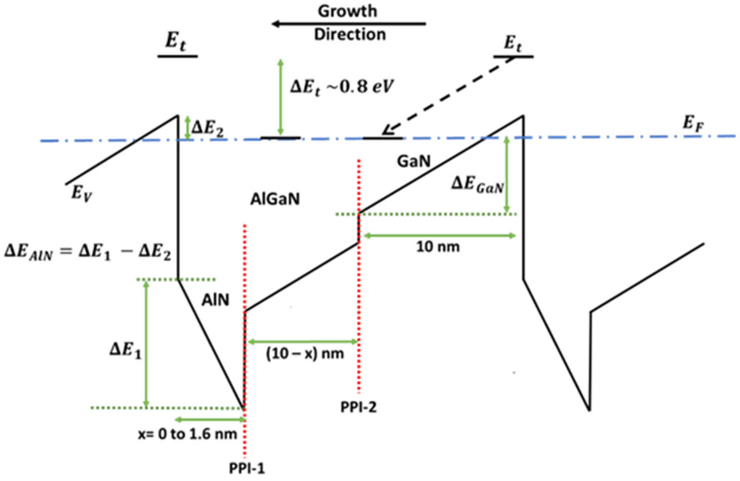
Figure 6.
A model valence band diagram schematic for a single p-type AlN/AlGaN/GaN SL period with low Mg doping. Et is the indicated acceptor trap level, with ΔEt = ~0.8 eV measured from the valence band (EV) of GaN. The arrow from Et indicates how the trap energy follows the band-bending and is just a guide to the eye. ΔE(AlN)(=ΔE1 − ΔE2 ≈ ΔE1) refers to band-bending in the AlN layer at the AlN/AlGaN interface, and ΔE(GaN) refers to band-bending in the GaN layer at the GaN/AlGaN interface. The vertical dotted lines indicate the two positive polarization interfaces (PPIs), in this case AlGaN/AlN (PPI-1) and GaN/AlGaN (PPI-2). The separation of these interfaces from the 2DHG is also shown in the diagram, and we used the reduced impact of hole mobility of traps ionized at PPI-2 (relative to PPI-1) because of the larger distance from the hole gas in order to support the analysis.
Following the methodology mentioned in [32], a proposed trap, 0.8 eV above the valence band of GaN (also referenced in all instances to the vacuum level, due to it being a deep trap) was invoked to resolve the presence of holes in excess of the Mg doping in the experiments. The level was chosen to be consistent with a Ga vacancy and some of its complexes in GaN. The existence of bulk traps is not ruled out, but the existence of a large concentration at positive polarization interfaces is proposed. When the band-bending of both GaN and AlN was <0.8 eV, the sheet charge concentration of holes (ps) measured using RT-Hall matched with the calculated values, as can be seen in Figure 3. For those samples where band-bending of either GaN or AlN was ≥0.8 eV (without accounting for the impact of trap ionization on band-bending), the measured ps was greater than the amount of Mg dopants put into the sample during growth. As an example, referencing Figure 3 from this work, for the sample series with Mg doping = 1 × 1019 cm−3, the measured and simulated hole concentrations match for samples with 0 nm and 0.7 nm AlN thickness, but for AlN thicknesses greater than that, the measured ps was greater than the simulated value and even higher than the amount of Mg dopants put into the sample during growth. This is because the band-bending of both GaN or AlN was ≥0.8 eV (without accounting for the impact of trap ionization on band-bending—in actuality, the Fermi level is pinned at the trap level), and hence the traps were ionized. The same logic holds true for all the other Mg doping series exhibited in Figure 3.
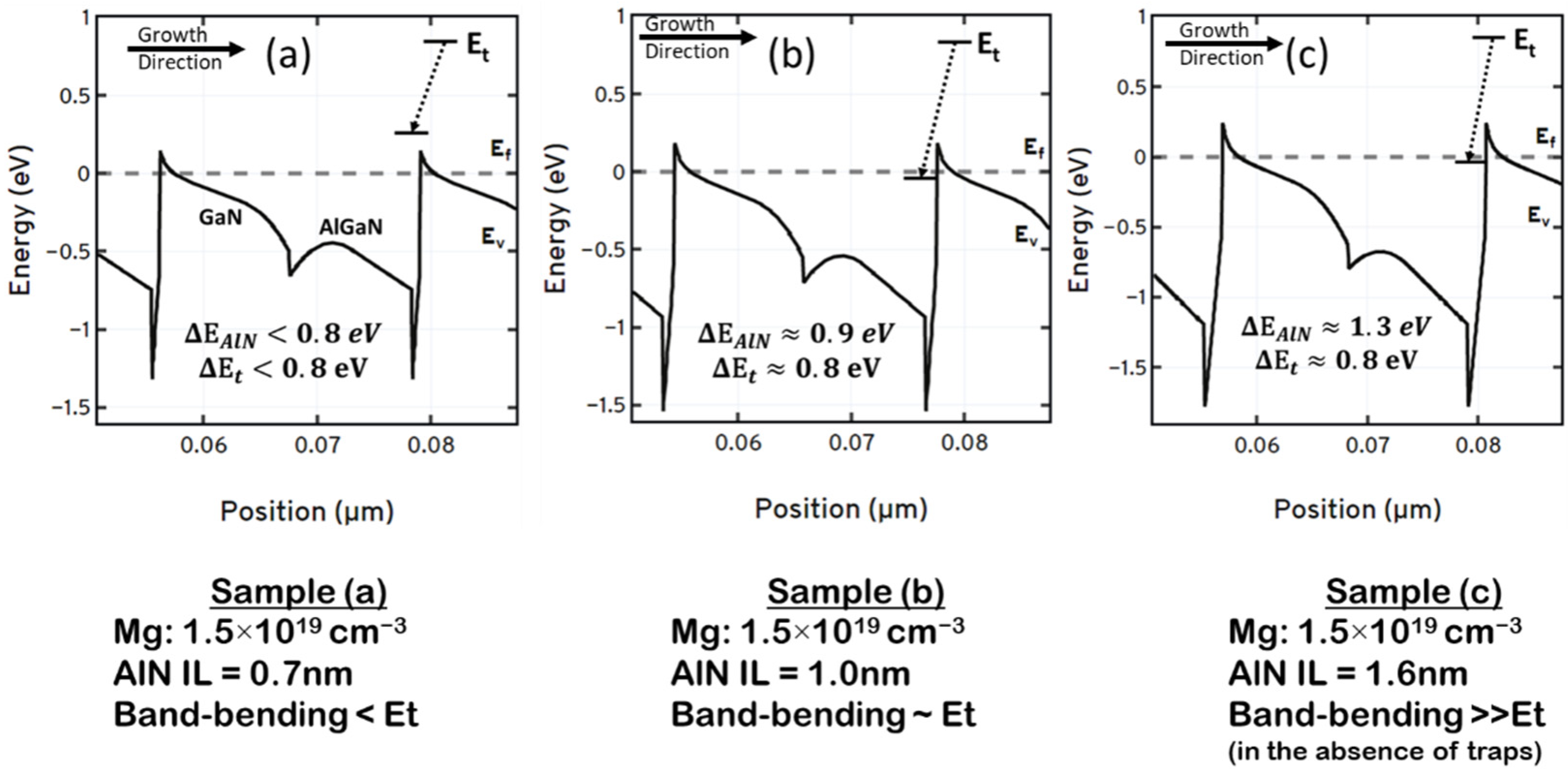
This consistent measurement confirms that the excess holes came from the acceptor traps at the positive polarization interfaces (PPIs), here AlGaN/AlN (PPI-1) and GaN/AlGaN (PPI-2) interfaces. The acceptor trap ionized when either band-bending was ≥0.8 eV and the Fermi level was consequently pinned at this trap level (=0.8 eV), leading to the high measured ps. Reference [32] elucidates this excess hole charge with simulations and experimental demonstrations for N-polar modulation doped SLs, while this study demonstrates the similar effect using the conventional Ga-polar uniformly doped p-type SLs and hence shows that these acceptor-like traps at the PPI in the III-nitride systems are agnostic to both polarity and doping schemes used. Low sheet resistance (~3 kΩ/sq) was observed for p-type Ga-polar uniformly doped AlGaN/AlN/GaN SLs, where trap states at only one or both interfaces were ionized. Figure 7 shows the actual band diagrams, with acceptor traps, simulated using the Silvaco package for a representative Mg doping of 1.5 × 1019 cm−3 and an AlN layer thickness of 0 nm, 1 nm, and 1.6 nm. Here the assumed acceptor trap concentration was 1 × 1013 cm−2 at each of the positive polarization interfaces, and this figure shows the Fermi level being pinned at the trap level when the either band-bending of GaN or AlN was ~0.8 eV and ionizes the acceptor-like trap.
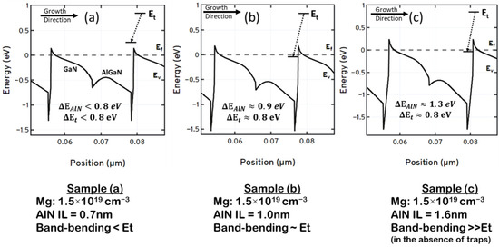
Figure 7.
Actual simulated valence band diagram using the Silvaco package, accounting for acceptor-like traps at positive polarization interfaces for samples (a–c) with Mg doping of 1.5 × 1019 cm−3 and AlN layer thickness of 0 nm, 1 nm, and 1.6 nm, respectively. In sample A, both band-bendings, ΔE(AlN) and ΔE(GaN), are less than 0.8 eV. In sample B, ΔE(GaN) is less than 0.8 eV, but ΔE(AlN) is ~0.9 eV, and so the acceptor-like trap ionizes. In (c), ΔE(AlN) is ~1.3 eV (from STR-FETIS), and so the acceptor-like trap ionizes. This shows that the trap hypothesis mentioned in this paper holds. The trap level, Et, is also indicated in the figure.
For the samples in this study, as shown in Figure 6, the existence of the two-dimensional hole gas (2DHG) is at the AlN/GaN interface (for AlGaN/AlN/GaN SL) or an AlGaN/GaN interface if no AlN is present (AlN interlayer (IL) thickness = 0 nm in Table 1). Table 1 indicates the samples presented in this work that have acceptor traps at the PPI ionizing, along with the interface where the traps ionized (PPI-1 or PPI-2). First, it was observed that for each of the AlN thickness series (with different Mg doping levels), the mobility values (μp) decreased in samples where the acceptor-like traps ionized. Within those sets of samples, it was further observed that μp decreased drastically (>40% decrease) in those samples where AlN band-bending was ≥0.8 eV, independent of the GaN band-bending level in the same sample. This could be explained by the fact that the 2DHG is closer to the AlGaN/AlN PPI, which is referred to as PPI-1 (0 to 1.6 nm), compared to the GaN/AlGaN PPI, referred to as PPI-2 (10 nm). Hence, the more dominant source of scattering (and therefore the cause of the drastic decrease in μp) is the ionized acceptor-like traps that exist at the AlGaN/AlN PPI, the interface that is closer to the 2DHG. The acceptor-like ionizing traps at the GaN/AlGaN PPI (PPI-2) also cause scattering, but their effect is not as pronounced because they are further away from the 2DHG. This explains the observed higher mobilities in samples where only the GaN band-bending was ≥0.8 eV and the AlN band-bending was <0.8 eV, leading to the ionization of traps at only PPI-2. This work presents 6 different series from our measurements, labeled A–F, based on the p-type Mg doping in the sample. Within each of those series, there are 5 samples with different AlN interlayer thicknesses from 0 to 1.6 nm. Analyzing each series of samples at a time, the main takeaway is that traps at PPI-1 (and hence AlN band-bending) determine whether the ionization of the acceptor-like trap drastically reduces the hole mobility, due to its proximity to the 2DHG (<1.6 nm away) compared to PPI-2 (10 nm away).
Figure 5 and Table 1 were used in tandem to describe the trends in mobility reported in the study and thereby substantiate the hypothesis and analysis. For series A, by design, all the epitaxially grown samples have the traps ionizing. In A-1 and A-2, only traps at PPI-2 are ionized, so the reduction in mobility is extremely negligible (Δ~1 cm2/Vs), caused by an increase in charge. Traps at both PPI-1 and PPI-2 are active in samples A-3, A-4, and A-5, and therefore the drastic mobility reduction can be seen going from A-1, A-2 to A-3, A-4, and A-5. In series B, sample B-1 does not have any traps ionized, but B-2 has only traps at PPI-2 ionized, resulting in an exceedingly small reduction in mobility (Δ~1 cm2/Vs), with the increase in hole charge causing it. B-3 through B-5 have traps at both PPI-1 and PPI-2 ionized, and thus we can see a drastic reduction in mobility going from B-1, B-2 to B-3, B-4, and B-5. In series-C, C-1 and C-2 do not have traps at any interface ionizing and we do not observe much reduction in mobility due to traps, although there is a slight decrease in mobility from C-1 to C-2 caused by the addition of the AlN IL and the increased polarization charge. C-3 through C-5 have traps at both PPI-1 and PPI-2 ionized, and thus we can see a huge reduction in mobility going from C-1, C-2 to C-3, C-4, and C-5, much like what happens with series B. In series-D, D-1 and D-2 do not have traps at any interface ionizing and we do not observe reduction in hole mobility due to traps. D-3 only has traps at PPI-1 ionized but not at PPI-2, and we see a huge reduction in mobility, which confirms our preliminary hypothesis. D-4 and D-5 have traps at both PPI-1 and PPI-2 ionizing, and there is a drastic reduction in mobility from D-1, D-2, but D-3, D-4, and D-5 have similar mobilities, which reiterates the dominant effect of traps at PPI-1. This is further confirmed in series-E: E-1, E-2, and E-3 do not have any traps ionizing, and we do not observe much reduction in mobility due to traps. E-4 has only traps at PPI-1 ionized but not PPI-2, and we see a huge reduction in mobility, which again confirms our preliminary hypothesis. E-5 has traps at both PPI-1 and PPI-2 ionizing, and there is a drastic reduction in mobility from E-1, E-2, and E-3, but E-4 and E-5 have similar mobilities. In series-F, F-1 to F-3 do not have any traps ionizing, but F4 and F5 have traps at PPI-1 ionizing, which reduces their mobility. On analyzing the series A–F, it can be inferred that the acceptor-like trap ionizing at the PPI closer to the 2DHG scatters the holes to a greater extent and hence has a major effect on reducing the μp. Note that these samples were all predictively designed such that the various interfaces were ionized per the hypothesis. The experimental data verify this particularly important hypothesis.
5. Conclusions
The results reported in this work use experimental results with energy band simulations to elucidate the effect of the ionization of acceptor-like traps on the total measured hole concentration and mobility of holes in III-nitrides. STR-FETIS was used for all band diagram calculations without taking any acceptor-like traps into account and for designing the experiment, and the Silvaco Atlas package was used to calculate the band diagrams after Hall effect measurements to simulate the actual band structures by including acceptor traps at positive polarization interfaces in the structure. One technique to resolve the actual nature of the trap levels and understand their identity is positron annihilation spectroscopy (PAS). This technique has been previously used to determine the nature of donor-like traps for corresponding n-type III-nitrides [37]. An elaborate PAS investigation of the p-type Ga-polar SLs reported in this work is currently underway, and the analysis will be reported in a separate study. The answer to how to get more holes in an epitaxially grown structure in p-type III-nitrides is interesting for its uses in both optoelectronics (for contact layers) and next-generation electronics (for GaN-based CMOS). The presence and subsequent experimental validity of these acceptor-like traps open up a novel method to engineer around III-nitride structures to achieve the desired total hole concentrations. The component of this study on traps at which PPIs have a major effect on the hole mobility provides an indication to design new LED and FET structures that can overcome the inherent challenges with holes in III-nitrides. All the samples reported in this study are Ga-polar, and this study, in conjunction with reports from Refs. [32,33], provide details of the existence of these acceptor traps in the III-nitride system agnostic to the polarity of the samples grown, and the doping scheme used, and also give a sense of universality to the existence of these acceptor traps at the PPI in the entire III-nitride material family.
Author Contributions
Conceptualization, A.K., A.R., S.K. and U.K.M.; methodology, A.K. and U.K.M.; electrical and Hall measurements, N.H., A.R. and A.K.; formal analysis, A.K.; writing—original draft preparation, A.K.; writing—review and editing, S.K. and U.K.M.; supervision, S.K. and U.K.M. All authors have read and agreed to the published version of the manuscript.
Funding
This work was supported by the Office of Naval Research (ONR) and ASCENT, one of six centers in JUMP, a Semiconductor Research Corporation (SRC) program sponsored by DARPA.
Institutional Review Board Statement
Not Applicable.
Informed Consent Statement
Not Applicable.
Data Availability Statement
The data that support the findings of this study are available within the article. More detailed findings of this study are available from the corresponding author upon reasonable request.
Conflicts of Interest
The authors declare no conflict of interest.
References
- Amano, H.; Baines, Y.; Beam, E.; Borga, M.; Bouchet, T.; Chalker, P.R.; Charles, M.; Chen, K.J.; Chowdhury, N.; Chu, R.; et al. The 2018 GaN Power Electronics Roadmap. J. Phys. D Appl. Phys. 2018, 51, 163001. [Google Scholar] [CrossRef]
- Baker, M.; Jain, S.; Shadmand, M.B. GaN Based High Frequency Power Electronic Interfaces: Challenges, Opportunities, and Research Roadmap. In Proceedings of the 2021 IEEE Power and Energy Conference at Illinois (PECI), San Diego, CA, USA, 1 April 2021; IEEE: Urbana, IL, USA, 2021; pp. 1–7. [Google Scholar]
- Chowdhury, S.; Swenson, B.L.; Wong, M.H.; Mishra, U.K. Current Status and Scope of Gallium Nitride-Based Vertical Transistors for High-Power Electronics Application. Semicond. Sci. Technol. 2013, 28, 074014. [Google Scholar] [CrossRef]
- Shrestha, P.; Guidry, M.; Romanczyk, B.; Karnaty, R.R.; Hatui, N.; Wurm, C.; Krishna, A.; Pasayat, S.S.; Keller, S.; Buckwalter, J.F.; et al. A Novel Concept Using Derivative Superposition at the Device-Level to Reduce Linearity Sensitivity to Bias in N-Polar GaN MISHEMT. In Proceedings of the 2020 Device Research Conference (DRC), Columbus, OH, USA, 21–24 June 2020; IEEE: Columbus, OH, USA, 2020; pp. 1–2. [Google Scholar] [CrossRef]
- Romanczyk, B.; Li, W.; Guidry, M.; Hatui, N.; Krishna, A.; Wurm, C.; Keller, S.; Mishra, U.K. N-Polar GaN-on-Sapphire Deep Recess HEMTs With High W-Band Power Density. IEEE Electron. Device Lett. 2020, 41, 1633–1636. [Google Scholar] [CrossRef]
- Romanczyk, B.; Zheng, X.; Guidry, M.; Li, H.; Hatui, N.; Wurm, C.; Krishna, A.; Ahmadi, E.; Keller, S.; Mishra, U.K. W-Band Power Performance of SiN-Passivated N-Polar GaN Deep Recess HEMTs. IEEE Electron. Device Lett. 2020, 41, 349–352. [Google Scholar] [CrossRef]
- Shrestha, P.; Guidry, M.; Romanczyk, B.; Hatui, N.; Wurm, C.; Krishna, A.; Pasayat, S.S.; Karnaty, R.R.; Keller, S.; Buckwalter, J.F.; et al. High Linearity and High Gain Performance of N-Polar GaN MIS-HEMT at 30 GHz. IEEE Electron. Device Lett. 2020, 41, 681–684. [Google Scholar] [CrossRef]
- Hatui, N.; Krishna, A.; Li, H.; Gupta, C.; Romanczyk, B.; Acker-James, D.; Ahmadi, E.; Keller, S.; Mishra, U.K. Ultra-High Silicon Doped N-Polar GaN Contact Layers Grown by Metal-Organic Chemical Vapor Deposition. Semicond. Sci. Technol. 2020, 35, 095002. [Google Scholar] [CrossRef]
- Sayed, I.; Liu, W.; Georgieva, J.; Krishna, A.; Keller, S.; Mishra, U.K. Characterization of AlSiO Dielectrics with Varying Silicon Composition for N-Polar GaN-Based Devices. Semicond. Sci. Technol. 2020, 35, 095027. [Google Scholar] [CrossRef]
- Ballestín-Fuertes, J.; Muñoz-Cruzado-Alba, J.; Sanz-Osorio, J.F.; Laporta-Puyal, E. Role of Wide Bandgap Materials in Power Electronics for Smart Grids Applications. Electronics 2021, 10, 677. [Google Scholar] [CrossRef]
- Nakamura, S.; Fasol, G. The Blue Laser Diode; Springer: Berlin, Heidelberg, 1997; ISBN 978-3-662-03464-4. [Google Scholar]
- Zhao, S.; Mi, Z. Recent Advances on P-Type III-Nitride Nanowires by Molecular Beam Epitaxy. Crystals 2017, 7, 268. [Google Scholar] [CrossRef]
- Asif Khan, M.; Shatalov, M.; Maruska, H.P.; Wang, H.M.; Kuokstis, E. III–Nitride UV Devices. Jpn. J. Appl. Phys. 2005, 44, 7191–7206. [Google Scholar] [CrossRef] [Green Version]
- Dahal, R.; Pantha, B.; Li, J.; Lin, J.Y.; Jiang, H.X. InGaN/GaN Multiple Quantum Well Solar Cells with Long Operating Wavelengths. Appl. Phys. Lett. 2009, 94, 063505. [Google Scholar] [CrossRef] [Green Version]
- Hurwitz, E.N.; Asghar, M.; Melton, A.; Kucukgok, B.; Su, L.; Orocz, M.; Jamil, M.; Lu, N.; Ferguson, I.T. Thermopower Study of GaN-Based Materials for Next-Generation Thermoelectric Devices and Applications. J. Electron. Mater. 2011, 40, 513–517. [Google Scholar] [CrossRef]
- Huang, Y.; Melton, A.; Jampana, B.; Jamil, M.; Ryou, J.-H.; Dupuis, R.D.; Ferguson, I.T. Compositional Instability in Strained InGaN Epitaxial Layers Induced by Kinetic Effects. J. Appl. Phys. 2011, 110, 064908. [Google Scholar] [CrossRef]
- Chatzakis, I.; Krishna, A.; Culbertson, J.; Sharac, N.; Giles, A.J.; Spencer, M.G.; Caldwell, J.D. Strong Confinement of Optical Fields Using Localized Surface Phonon Polaritons in Cubic Boron Nitride. Opt. Lett. 2018, 43, 2177. [Google Scholar] [CrossRef]
- Fragkos, I.E.; Tansu, N. Surface Plasmon Coupling in GaN: Eu Light Emitters with Metal-Nitrides. Sci. Rep. 2018, 8, 13365. [Google Scholar] [CrossRef]
- Zhou, C.; Ghods, A.; Saravade, V.G.; Patel, P.V.; Yunghans, K.L.; Ferguson, C.; Feng, Y.; Kucukgok, B.; Lu, N.; Ferguson, I.T. Review—The Current and Emerging Applications of the III-Nitrides. ECS J. Solid State Sci. Technol. 2017, 6, Q149. [Google Scholar] [CrossRef] [Green Version]
- Kako, S.; Santori, C.; Hoshino, K.; Götzinger, S.; Yamamoto, Y.; Arakawa, Y. A Gallium Nitride Single-Photon Source Operating at 200 K. Nat. Mater. 2006, 5, 887–892. [Google Scholar] [CrossRef]
- Quay, R. Gallium Nitride Electronics; Springer Series in Materials Science; Springer: Berlin, Germany, 2008; ISBN 978-3-540-71890-1. [Google Scholar]
- Hatui, N.; Krishna, A.; Pasayat, S.S.; Keller, S.; Mishra, U.K. Metal Organic Vapor Phase Epitaxy of Thick N-Polar InGaN Films. Electronics 2021, 10, 1182. [Google Scholar] [CrossRef]
- Chu, R.; Cao, Y.; Chen, M.; Li, R.; Zehnder, D. An Experimental Demonstration of GaN CMOS Technology. IEEE Electron. Device Lett. 2016, 37, 269–271. [Google Scholar] [CrossRef]
- Bader, S.J.; Chaudhuri, R.; Nomoto, K.; Hickman, A.; Chen, Z.; Then, H.W.; Muller, D.A.; Xing, H.G.; Jena, D. Gate-Recessed E-Mode p-Channel HFET With High On-Current Based on GaN/AlN 2D Hole Gas. IEEE Electron. Device Lett. 2018, 39, 1848–1851. [Google Scholar] [CrossRef] [Green Version]
- Arakawa, Y.; Ueno, K.; Kobayashi, A.; Ohta, J.; Fujioka, H. High Hole Mobility P-Type GaN with Low Residual Hydrogen Concentration Prepared by Pulsed Sputtering. APL Mater. 2016, 4, 086103. [Google Scholar] [CrossRef] [Green Version]
- Chowdhury, N.; Xie, Q.; Yuan, M.; Cheng, K.; Then, H.W.; Palacios, T. Regrowth-Free GaN-Based Complementary Logic on a Si Substrate. IEEE Electron. Device Lett. 2020, 41, 820–823. [Google Scholar] [CrossRef]
- Krishna, A.; Raj, A.; Hatui, N.; Koksaldi, O.; Jang, R.; Keller, S.; Mishra, U.K. AlGaN/GaN Superlattice-Based P-Type Field-Effect Transistor with Tetramethylammonium Hydroxide Treatment. Phys. Status Solidi A 2020, 217, 1900692. [Google Scholar] [CrossRef]
- Raj, A.; Krishna, A.; Hatui, N.; Gupta, C.; Jang, R.; Keller, S.; Mishra, U.K. Demonstration of a GaN/AlGaN Superlattice-Based p-Channel FinFET With High ON-Current. IEEE Electron. Device Lett. 2020, 41, 220–223. [Google Scholar] [CrossRef]
- Pampili, P.; Parbrook, P.J. Doping of III-Nitride Materials. Mater. Sci. Semicond. Process. 2017, 62, 180–191. [Google Scholar] [CrossRef]
- Kozodoy, P.; Smorchkova, Y.P.; Hansen, M.; Xing, H.; DenBaars, S.P.; Mishra, U.K.; Saxler, A.W.; Perrin, R.; Mitchel, W.C. Polarization-Enhanced Mg Doping of AlGaN/GaN Superlattices. Appl. Phys. Lett. 1999, 75, 2444–2446. [Google Scholar] [CrossRef]
- Raj, A.; Krishna, A.; Hatui, N.; Romanczyk, B.; Wurm, C.; Guidry, M.; Hamwey, R.; Pakala, N.; Keller, S.; Mishra, U.K. GaN/AlGaN Superlattice Based E-Mode p-Channel MES-FinFET with Regrown Contacts and >50 MA/Mm on-Current. In Proceedings of the 2021 IEEE International Electron Devices Meeting (IEDM), San Francisco, CA, USA, 11 December 2021; IEEE: San Francisco, CA, USA, 2021; pp. 5.4.1–5.4.4. [Google Scholar] [CrossRef]
- Krishna, A.; Raj, A.; Hatui, N.; Sayed, I.; Keller, S.; Mishra, U.K. Proposed Existence of Acceptor-like Traps at Positive Polarization Interfaces in p-Type III-Nitride Semiconductors. Appl. Phys. Lett. 2020, 117, 042104. [Google Scholar] [CrossRef]
- Krishna, A.; Raj, A.; Hatui, N.; Keller, S.; Denbaars, S.; Mishra, U.K. Acceptor Traps as the Source of Holes in P-Type N-Polar GaN/(AlN/AlGaN) Superlattices. Appl. Phys. Lett. 2022, 120, 132104. [Google Scholar] [CrossRef]
- Krishna, A.; Raj, A.; Hatui, N.; Keller, S.; Mishra, U.K. Investigation of Nitrogen Polar P-Type Doped GaN/AlxGa(1-x)N Superlattices for Applications in Wide-Bandgap p-Type Field Effect Transistors. Appl. Phys. Lett. 2019, 115, 172105. [Google Scholar] [CrossRef] [Green Version]
- Lund, C.; Agarwal, A.; Romanczyk, B.; Mates, T.; Nakamura, S.; DenBaars, S.P.; Mishra, U.K.; Keller, S. Investigation of Mg δ -Doping for Low Resistance N-Polar p-GaN Films Grown at Reduced Temperatures by MOCVD. Semicond. Sci. Technol. 2018, 33, 095014. [Google Scholar] [CrossRef]
- Fichtenbaum, N.A.; Mates, T.E.; Keller, S.; DenBaars, S.P.; Mishra, U.K. Impurity Incorporation in Heteroepitaxial N-Face and Ga-Face GaN Films Grown by Metalorganic Chemical Vapor Deposition. J. Cryst. Growth 2008, 310, 1124–1131. [Google Scholar] [CrossRef]
- Prozheeva, V.; Makkonen, I.; Li, H.; Keller, S.; Mishra, U.K.; Tuomisto, F. Interfacial N Vacancies in Ga N/(Al, Ga) N/Ga N Heterostructures. Phys. Rev. Appl. 2020, 13, 044034. [Google Scholar] [CrossRef]

Publisher’s Note: MDPI stays neutral with regard to jurisdictional claims in published maps and institutional affiliations. |
© 2022 by the authors. Licensee MDPI, Basel, Switzerland. This article is an open access article distributed under the terms and conditions of the Creative Commons Attribution (CC BY) license (https://creativecommons.org/licenses/by/4.0/).