Article

The Potential Effect of Annealing Mesostructured Titanium Dioxide Electrode in a Closed Box Furnace on the Concentration of Lead (II) Iodide Solution Required for Optimal Performance of Mesoscopic Perovskite Solar Cells

1
Department of Materials Engineering, School of Chemical & Materials Engineering, National University of Science & Technology (NUST), H-12 Sector, Islamabad 44000, Pakistan
2
Laboratory of Molecular Science & Engineering, Faculty of Science & Engineering (FNT), Åbo Akademi University, Henrikinkatu 2, FI-20500 Turku, Finland
*
Author to whom correspondence should be addressed.
Crystals 2022, 12(6), 833; https://doi.org/10.3390/cryst12060833
Submission received: 2 May 2022 / Revised: 26 May 2022 / Accepted: 30 May 2022 / Published: 12 June 2022

Abstract

:
Highly reproducible mesoscopic perovskite solar cells (PSCs) can be fabricated using two-step sequential deposition of organo-lead halide (perovskite) active layer. However, differences in the processing conditions of individual layers which are subsequently assembled to construct the ultimate device can result in variations in the solar cell performance. For instance, here we report trends in the device performance as a function of PbI2 solution concentration, where the compact and mesoporous TiO2 layers were annealed in a closed box furnace (instead of doing it in open air). We observed that the devices prepared using 1.2 M PbI2 solution concentration performed better than those prepared from 0.8 M and 1 M PbI2 solutions. Generally, the researchers use the hot plate in an open-air environment or use a special hot plate where a continuous flow of air is ensured while annealing TiO2 electron selective layers (ESL) for perovskite solar cells. In this case, the highest possible device efficiencies are achieved using 1 M concentration of PbI2 solution. Although the influence of PbI2 solution concentration has been previously studied in detail, here our prime focus is to briefly comment on slight differences in the device performance trends which we observed in comparison to the previously reported results, where TiO2 layers were calcined in open air.

1. Introduction

Solar energy is freely and abundantly available form of energy which can be effectively used for electricity generation using solar cells. The solar cells based on crystalline silicon are well commercialized and known to be reliable because they are technologically mature in comparison to other types of photovoltaic devices. However, highly energy intensive and expensive processing methods required for manufacturing silicon wafers have pushed the scientific community to look for some other alternatives such as perovskite solar cells (PSCs). The high-power conversion efficiencies (PCEs) of PSCs are known to be very comparable to those of silicon-based solar cells. The fabrication of PSCs is also known to be very cost-effective due to their solution-processability. Earlier research in this area depended on one-step deposition of perovskite active layer, in which a mixed precursor single solution was spin-coated on top of the substrate [1]. The synthesis of the active layer using a one-step approach would result in its highly non-uniform coverage on top of the substrate, thus large number of parallel shunts would deteriorate the device performance and its reproducibility. The introduction of two-step sequential deposition of the perovskite active layer by Burschka et al. [2] significantly solved this problem. In this method, the lead halide solution was spin-coated, followed by dropping the Methylammonium halide solution on top of the rotating substrate [3,4] or immersing the lead halide coated substrate into the Methylammonium halide solution [2]. There were still issues with this method, because to bring their PCEs beyond 15 to 16% required major modifications, such as interdiffusion strategy. This is generally because of the incomplete conversion of PbI2 to perovskite upon reaction with MAI, which results in a considerable amount of unreacted PbI2 in the deeper regions of perovskite active layer [5]. To further enhance the device efficiencies, one-step deposition was again introduced, but this time it involved dropping the Chlorobenzene [6,7] or Toluene [8] as anti-solvents on top of the rotating substrate comprising of single precursor solution. The anti-solvent approach potentially produces high-efficiency devices, but still suffers from reproducibility issues. This is because this route is highly delicate and sensitive to handling and deposition conditions [9]. Thus, the two-step deposition technique is relatively more tolerant to such issues and therefore highly reproducible, with some compromise on the device efficiencies owing to the presence of residual PbI2 in the perovskite active layer.
On the other hand, this unreacted PbI2 is also known to be beneficial for the passivation of interfacial defects at the perovskite/metal oxide electrode interface [10]. However, there is always some critical amount of unconverted PbI2 in the perovskite active layer beyond which device performance starts to deteriorate. The amount of unconverted PbI2 in the perovskite can be controlled either by controlling the PbI2 solution concentration while keeping the concentration of MAI solution constant, or vice versa [11]. The optimal device performance with the two-step approach can be achieved by keeping the PbI2 and MAI solution concentrations as 1 M and 0.063 M, respectively. Tuning the MAI solution concentration significantly influences the crystal size of the perovskite active layer, thus bulk recombination can be somehow minimized by reducing the number of grain boundaries. On the other hand, the PbI2 concentration influences the morphology of the perovskite capping layer on top of the mesostructured substrate [11,12].
Several research works performed in the past few years investigated the influence of PbI2 and MAI solution concentrations. Here, we also present the effect of PbI2 solution concentration on the device performance, though we will discuss some differences in trends we observed as a function of PbI2 concentration in comparison to the previously reported results which suggested that 1 M PbI2 solution is most suitable for the optimal device performance. We used three different concentrations of the PbI2 solution, i.e., 0.8 M, 1 M and 1.2 M, respectively. The solar cells prepared using 1.2 M PbI2 solution were found to perform unexpectedly better than the devices prepared using 1 M PbI2 solution. However, it is a well-known fact that 1 M concentration of PbI2 solution is best for the optimal performance of PSCs. Our XRD results also revealed that the residual PbI2 content in the perovskite films prepared using 1.2 M PbI2 solution is significantly higher. Thus, one should expect that the lower perovskite content in 1.2 M sample should ideally not be able to give enough photogenerated electricity. Surprisingly, the VOC values of the devices based on 1.2 M PbI2 concentration were found to be significantly higher than those prepared using 1 M concentration of PbI2 solution. We suspect that the mesoporous TiO2 used as a scaffold in this work contains very high concentration of oxygen vacancies because we used a closed box furnace for its calcination with no continuous air flow. This has been previously demonstrated by Ho et al. [13], that a continuous oxygen-rich air flow is required during the calcination of TiO2 films to minimize oxygen defects which can be the ultimate source of surface recombination at the TiO2/Perovskite interface [14]. Oxygen defects at the surface of TiO2 thin films can also be reduced using UV-ozone treatment [15]. The presence of oxygen vacancies tends to disrupt the entire stoichiometric balance on both sides of the TiO2/Perovskite interface. This results in partial breaking up of Pb-I bonds of the perovskite close to the interface. Thus, there are defects in the perovskite as well as in the TiO2. The defects in perovskite tend to capture the photogenerated electrons within the perovskite, which can potentially reduce the JSC. On the other hand, interfacial trap states due to the oxygen vacancies in TiO2 captures the injected electrons which subsequently recombine with the holes in VB of the perovskite (because of electron back transfer) which ultimately reduces the VOC [14]. Since we expect that our (compact and mesoporous) TiO2 comprises of higher density of oxygen vacancies, their effective passivation requires much larger quantity of unreacted (or residual) PbI2 at the perovskite/TiO2 interface. This is possible by using higher PbI2 solution concentration (such as 1.2 M) than previously optimized concentration (i.e., 1 M).

2. Materials and Methods

2.1. Materials

Fluorine-doped Tin Oxide coated glass substrates (TCO22-15) were purchased from Solaronix (Aubonne, Switzerland). TiCl4 (>99%) was bought from Fluka (Seelze, Germany). Pluronic F127 block co-polymers, tetrahydrofuran (THF, >99%), N,N-dimethylformamide (DMF, 99.8%), 2-propanol (99.5%), chlorobenzene (99.8%), acetonitrile (99.8%), and Lithium bis(trifluoromethane)sulfonimide (Li-TFSI), were purchased from Sigma Aldrich (St. Louis, MO, USA). The PbI2 (99.99%) and Methylammonium Iodide, MAI (>98%) were acquired from TCI Europe (Zwijndrecht, Belgium) and spiro-OMeTAD from Feiming Chemicals Ltd (Shenzhen, China). The cobalt (III) tri[bis-(trifluromethane]sulfonamide) (FK209 Cobalt (III) salt) and 30 NR-D TiO2 paste were obtained from Greatcell (Queanbeyan, Australia). Ethanol (EtOH, >99.5%) was bought from ALTIA Plc, Helsinki, Finland.

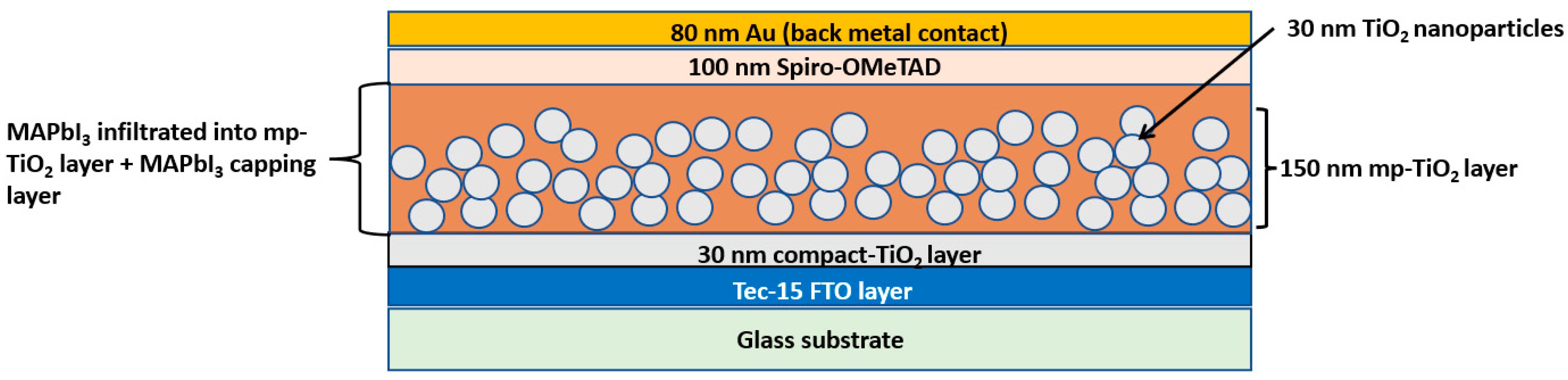
2.2. Preparation of Compact and Mesoporous TiO2 Films

The compact TiO2 (c-TiO2) dip coating solution was prepared as previously reported by Masood et al. [16]. For this, a TiCl4/EtOH stock solution was prepared by dropwise addition of 18.97 g of TiCl4 into 23.04 g of EtOH while stirring in an ice bath. Another solution comprising of 0.0152 g of F127 block co-polymer, 12.34 g of EtOH, 0.21 g of deionized water and 1.717 g of THF was prepared. Thereafter, 2.50 g of the TiCl4/EtOH stock solution was added dropwise into the second solution and kept for stirring for at least 30 min before dip coating the FTO coated glass substrates.
The FTO coated glass substrates were cut into 4 cm × 2 cm pieces. A 1.5 cm × 2 cm area was etched from one side of the FTO substrates using Zn powder and 4 M aqueous solution of HCl. The substrates were sonicated in 2% aqueous Halmanex III solution, de-ionized water, Acetone and 2-propanol for 10 min each. After drying the substrates by blowing dry Nitrogen, they were further subjected to plasma treatment for 5 min before dip-coating in the c-TiO2 solution. For dip-coating, the withdrawal speed of 85 mm/min was used without allowing any dwell time in the solution. The c-TiO2 substrates were then dried on the hot plate at 125 °C followed by direct calcination at 500 °C for 30 min in the closed box furnace. To study the perovskite filled mesostructured TiO2 (by XRD, UV-Vis and FE-SEM), the unetched FTO coated glass substrates were used. The subsequent mesoporous TiO2 layer was deposited as a scaffold, thus preparing the mp-TiO2/c-TiO2/FTO/glass substrates. For this purpose, the suspension of TiO2 nanoparticles was prepared by dissolving 30 NR-D TiO2 paste (from Greatcell) in Ethanol (EtOH) to maintain the concentration of 0.15 g/mL. After applying plasma treatment on top of c-TiO2/FTO/glass substrates, the mesoporous TiO2 solution was spin-coated using 4000 rpm spin speed for 10 s. The spin acceleration was set to 2000 rpm/s. The films were then dried on the hot plate at 120 °C for 10 min before calcination at 450 °C for 30 min by following the previously reported heating ramp [16,17].

2.3. Deposition of the Perovskite Active Layer

Next, 0.8 M, 1 M and 1.2 M PbI2 solutions were prepared in anhydrous DMF while stirring at 100 °C on hot plate. The solutions were kept at 100 °C throughout the experiment to prevent precipitation of PbI2 crystals within the solutions. The PbI2 solutions were spin-coated on the mesostructured TiO2 substrates with a spin speed of 6000 rpm for 30 s using 6100 rpm/s acceleration rate. The PbI2-coated substrates were dried on a hot plate at 100 °C for 30 min. Upon subsequent cooling to room temperature, the substrates were dipped in 10 mg/mL solution of MAI dissolved in anhydrous isopropanol followed by quick rinsing in isopropanol to remove excess MAI. The substrates were again dried at 100 °C for 30 min on the hot plate.

2.4. Characterization

The Grazing incidence X-ray diffraction (GI-XRD) was performed on all the perovskite infiltrated mesostructured TiO2 (i.e., mp-TiO2/c-TiO2/unetched-FTO/glass) substrates. This was carried out to verify the differences in the relative amount of perovskite with respect to the unreacted PbI2 as a function of PbI2 solution concentration. This was achieved using Bruker AXS D8 Discover instrument (Billerica, MA, USA). The Bragg’s angle scan was performed between 10° to 20° using 0.04° step size at grazing incidence angle of 1°. The UV-visible (UV-vis) absorption scan was also performed on these samples between 300 to 900 nm wavelength range using Perkin Elmer Lambda 900 UV-vis near infrared spectrometer (Waltham, MA, USA). The slit size was kept at 2 mm and the measurements were performed in the presence of certified reflectance standards. The UV-Vis measurements were also performed on PbI2 infiltrated mesostructured TiO2 (mp-TiO2/glass) substrates as a reference.
To assess the morphology of PbI2 and perovskite capping layers on top of the mesostructured TiO2 layer, the field emission scanning electron microscopy (LEO, Oberkochen, Germany) was performed. For this purpose, the 50 k times magnification, 2.70 kV electron high tension and an aperture size of 10 μm were used.

2.5. Device Fabrication

The lab-scale devices were prepared using different PbI2 concentrations by following our previously reported protocol [16]. Figure 1 schematically shows the structure of our typical device.
The etching of FTO, and the deposition of compact and mesoporous TiO2 layers has already been explained in Section 2.2. Three to four devices for each PbI2 concentration were fabricated. After depositing the perovskite active layer, as mentioned in Section 2.3, the spiro-OMeTAD and 4-tertbutyilpyridine were dissolved in chlorobenzene. On the other hand, the solutions of Lithium bis(trifluoromethylsulfonyl)imide and FK209 Co(III) were prepared by dissolving them in acetonitrile. These solutions were then added to the solution of Spiro-MeTAD. This was carried out to maintain the molar ratio of 1.0:0.5:2.5 × 10⁻²:3.3:131.5:7.2 (spiro-MeTAD: Li-TFSI: FK209 Co (III): 4-tertbutylpyridine: chlorobenzene: acetonitrile). The final solution was then spin-coated on top of the perovskite active layer using a spin speed of 4000 rpm for 30 s with 4000 rpm/s spin acceleration. The circular gold back metal contacts of area 0.283 cm2 were deposited on top of the Sprio-OMeTAD layer. This was achieved by evaporating gold at an evaporation rate of about 0.01 nm/s while keeping the vacuum pressure of about 2 × 10⁻⁵ mbar.

2.6. Device Characterization

The J-V curves were measured in ambient conditions under illumination using a simulated sunlight at AM 1.5 with 100 mW/cm2 intensity (Oriel Class ABB solar simulator, 150 W, 2″ × 2″). A circular aperture with the size of about 0.126 cm2 was used to mask the devices. The J-V scan was performed using a 2636 Series Source Meter (Keithley instruments, Cleveland, OH, USA)—The scan was started from −0.3 V to 1.1 V in forward sweep followed by 1.1 V to −0.3 V in reverse sweep using a scan speed of about 10 mV/S [17]. For each PbI2 concentration at least 3 to 4 devices were characterized to determine the photovoltaic parameters.

3. Results

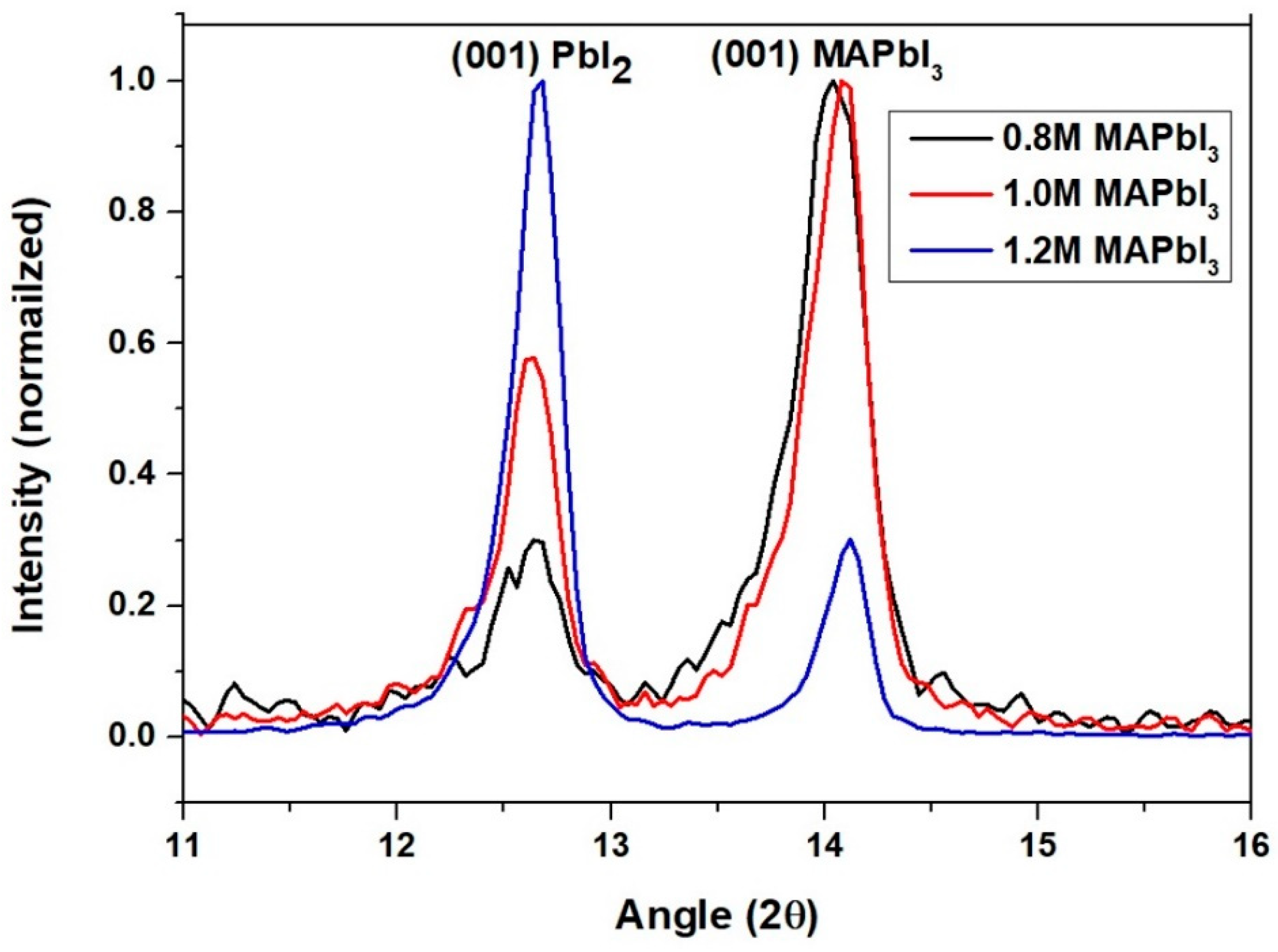
3.1. Determining the Perovskite Content Using GI-XRD

We started by analyzing the influence of PbI2 solution concentration on PbI2-to-MAPbI3 conversion efficiency in PbI2 infiltrated mesostructured TiO2 substrates (when dipped in 0.063 M MAI solution, as discussed in Section 2.3). This was carried out by performing GI-XRD using 1° incident angle upon each sample after it was converted to the perovskite. The diffractograms from GI-XRD were then normalized to further determine the relative amounts of remnant PbI2 and the perovskite. The samples in the subsequent text are named according to the concentration of PbI2 solutions. The samples without conversion to the perovskite were named as 0.8 M PbI2, 1.0 M PbI2 and 1.2 M PbI2. The samples after conversion to the perovskite were named as 0.8 M MAPbI3, 1.0 M MAPbI3 and 1.2 M MAPbI3.
The normalized GI-XRD diffractograms are shown in Figure 2, where all the perovskite samples contain both the perovskite (MAPbI3) and the unreacted residual PbI2. This is evident from PbI2 (001) and MAPbI3 (110) reflections at 12.6° and 14.1° angles, respectively.
The unreacted PbI2 is left in the deeper regions of all the perovskite samples because MAI is not able to reach those areas to react and form MAPbI3 [17]. Using areas under each reflection, we calculated the percentage of perovskite (MAPbI3) in each sample based on different PbI2 solution concentrations. Areas under each reflection were calculated by integration and then by using the following formula, and the percentage of perovskite in each sample was calculated:
%   P e r o v s k i t e = A r e a   u n d e r   M A P b I 3 ( 110 )   p e a k A r e a   u n d e r   M A P b I 3 ( 110 )   p e a k + A r e a   u n d e r   P b I 2 ( 001 ) p e a k × 100 %
The percentage perovskite can be used as a measure of PbI2-to-MAPbI3 conversion efficiency. A higher percentage of perovskite (MAPbI3) peak is a sign of better conversion efficiency and vice versa. Table 1 shows the percentage perovskite values calculated from Figure 2.
The trend in these values demonstrates that that the PbI2-to-MAPbI3 conversion is suppressed upon increasing the concentration of PbI2 solution, which is absolutely expected. This is because, moving towards increased concentration of PbI2 solution means increased and dense crystallization of PbI2 within the mesostructured layer. Therefore, PbI2 in the deeper regions of mesostructured TiO2 is not accessible for Methylammonium Iodide (MAI) (when dipped in the MAI solution). An elaborate discussion regarding the PbI2-to-MAPbI3 conversion can be found in one of our previous works [17].

3.2. Influence of PbI2 on the Absorbance before and after Conversion to MAPbI3

The samples were further analyzed using UV-Vis spectroscopy and the resulting spectra are shown in Figure 3.
The dotted lines show the spectra corresponding to the mesostructured TiO2 substrates infiltrated with PbI2 by spin-coating solutions of different PbI2 concentrations. The same figure also shows the spectra of MAPbI3 corresponding to the samples with three different PbI2 concentrations. The spectra corresponding to the PbI2 loaded films reveals that increasing PbI2 concentration from 0.8 to 1 M results in a significant increase in the absorbance below 500 nm wavelength. However, further increase in the concentration to 1.2 M does not result in any noticeable change. This is probably because increasing the PbI2 concentration results in increased loading of mesostructured TiO2 with PbI2, which is densely crystallized within the porous channels and in the form of capping layer. Going beyond 1 M concentration results in the removal of excess PbI2 during spinning process. In other words, there is a limit, beyond which further loading of mesostructured TiO2 films with PbI2 is not possible, hence we do not see any further increase in absorbance when moving from 1 to 1.2 M PbI2 loaded mesostructured TiO2. Contrary to this, using lower concentrations of PbI2 (such as 0.8 M) probably results in sparse crystallization of PbI2 within the porous channels of mesostructured TiO2.
The perovskite (MAPbI3) corresponding to the 1 M PbI2 concentration shows highest absorbance over the entire wavelength range while lowest absorbance (above 440 nm wavelength) is achieved for the perovskite prepared from 1.2 M PbI2 solution. Our results agree with Wang et al. [11], who also performed similar measurements on ZnO doped TiO2 nanostructured films loaded with MAPbI3 prepared from different PbI2 concentrations.
In general, these results suggest that 1 M PbI2 concentration is most suitable for optimal conversion to MAPbI3 using 0.063 M MAI solution. Although the highest PbI2-to-MAPbI3 conversion percentage is achieved for 0.8 M MAPbI3 sample (based on GI-XRD results), its absorbance is still lower in comparison to the1 M MAPbI3. This indicates that the overall amount of perovskite in the 0.8 M MAPbI3 is still lower in comparison to the perovskite prepared using 1 M PbI2 concentration. The absorbance of 1.2 M MAPbI3 is even inferior to 0.8 M MAPbI3 and 1 M MAPbI3 samples within the visible range. This is due to its poorest PbI2-to-MAPbI3 conversion efficiency. Thus, it can be stated for sure that the overall amount of perovskite in 1 M MAPbI3 sample is still higher than the perovskite in 0.8 M and 1.2 M samples.

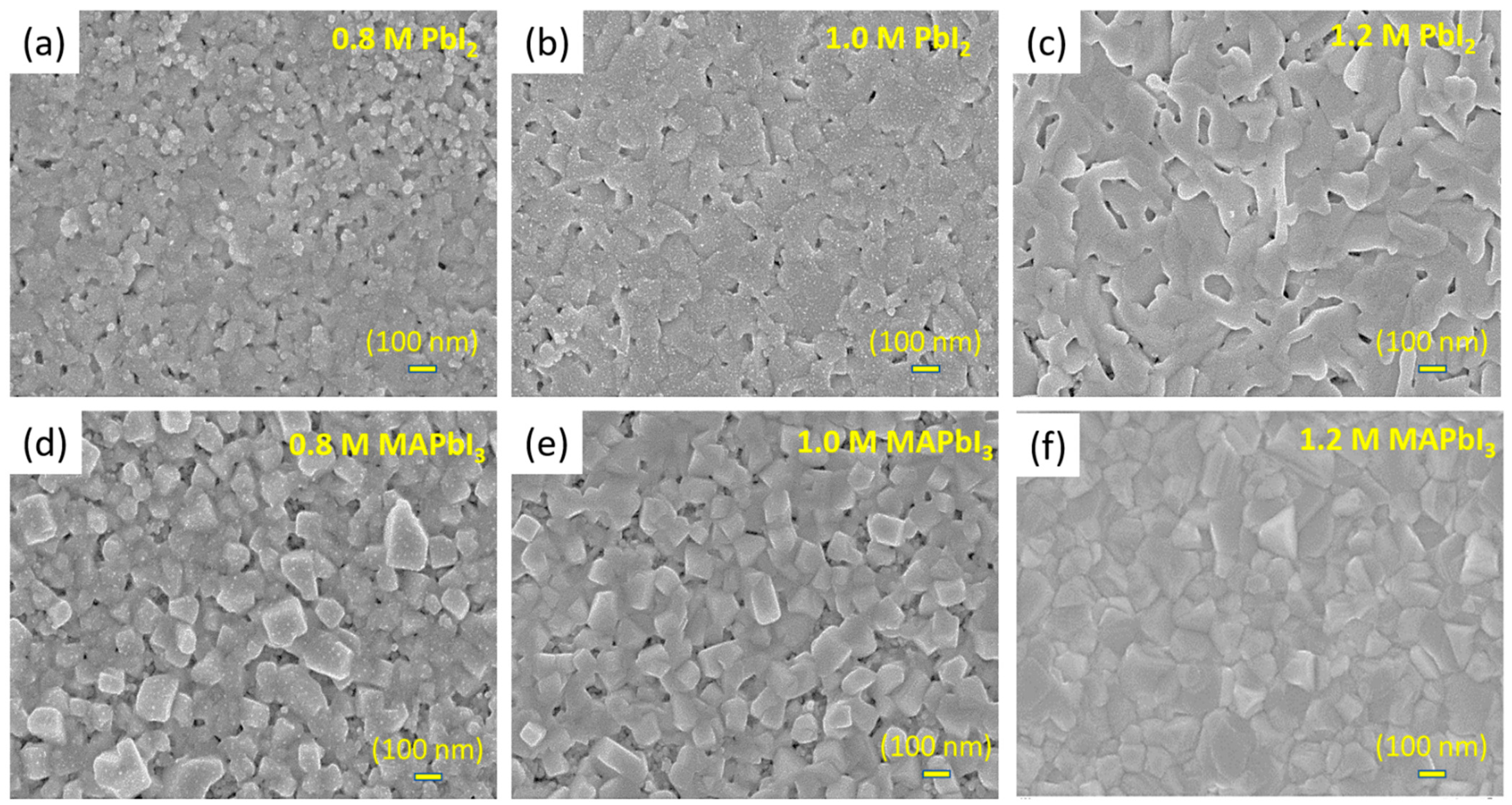
3.3. Morphology of the Capping Layer before and after Conversion to MAPbI3

Figure 4 shows the SEM images of PbI2 coated mesostructured TiO2 substrates prepared using three different PbI2 concentrations and their corresponding MAPbI3 perovskite samples (after conversion).
It is evident from Figure 4a that the complete coverage of PbI2 capping layer could not be achieved in 0.8 M PbI2 sample. This is because this PbI2 concentration is barely sufficient to fill in the pores while its capping layer can partially cover the mesoporous TiO2 layer. The underlying TiO2 nanoparticles left uncovered by PbI2 capping layer are also visible as white spots in Figure 4a. For 1 M and 1.2 M PbI2 samples (shown in Figure 4b,c, respectively), the PbI2 capping layer completely covers the underlying mesostructured TiO2.
The SEM images of corresponding 0.8 M, 1 M and 1.2 M MAPbI3 samples are shown in Figure 4d–f, respectively. The pinholes in the perovskite capping layer are clearly visible for 0.8 M and 1 M MAPbI3 samples. These pinholes may allow the infiltration of subsequent hole selective layer (HSL) down to the underlying mesostructured TiO2 during its deposition process and enable the formation of parallel shunts to deteriorate the device performance. However, the complete coverage of the perovskite capping layer is achieved using 1.2 M concentration of PbI2 (i.e., for 1.2 M MAPbI3 sample shown in Figure 4f). This could possibly have significant contribution to the trends in the device performance as a function of PbI2 concentration (typically the VOC values).
Based on GI-XRD, UV-Vis and SEM results, increased PbI2 concentration results in increased loading of mesostructured TiO2. In other words, filling up of the empty spaces within the mesostructured TiO2 by PbI2 is proportional to the PbI2 solution concentration. PbI2 may also densely fill in the voids between TiO2 nanoparticles upon using even higher concentration of PbI2 solution such as 1.2 M.
Increased loading of PbI2 within the mesostructured TiO2 can be beneficial in terms of achieving higher perovskite content, provided that the PbI2 is not densely crystallized within the porous channels. This is because PbI2 in deeper regions should be accessible for effective reaction with MAI to form MAPbI3. If PbI2 is densely crystallized within the pores, MAI will not be able to reach PbI2 lying in the deeper regions of mesostructured TiO2 for complete reaction. It is also possible that the conversion is even restricted to the capping layer region with little conversion near the pore openings. This seems to be more obvious for 1.2 M MAPbI3 sample in Figure 2 (GI-XRD diffractogram). On the other hand, using lower PbI2 concentration (such as 0.8 M) may result in sparse crystallization of PbI2 within the pores. Therefore, PbI2 crystallized in deeper region of the porous channels are more accessible for MAI to react. Therefore, the conversion of PbI2-to-MAPbI3 is more efficient for lower PbI2 concentration, and vice versa.

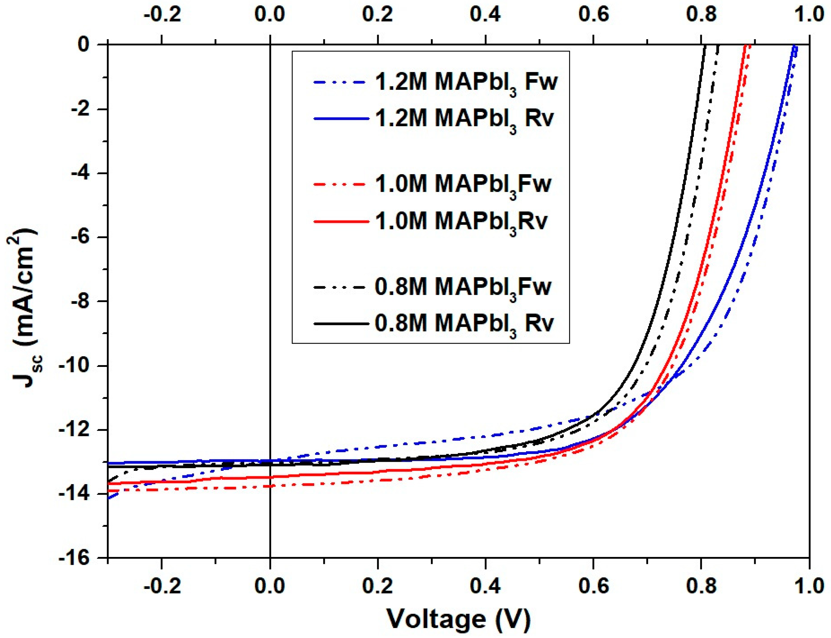
3.4. The Influence of PbI2 Concentration on the Device Performance

The devices were prepared using a perovskite absorber based on three different PbI2 concentrations. Figure 5 shows the light J-V curves under forward and reverse sweep for the devices performing close to average power conversion efficiencies (PCEs). Three to four devices were analyzed for each PbI2 concentration to tabulate the mean and standard deviation for each photovoltaic parameter shown in Table 2.
The table shows decreasing trends in the fill factor with increase in PbI2 concentration. This decreasing trend is more obvious upon increasing PbI2 concentration from 0.8 to 1 M. This means that an increased amount of unreacted PbI2 in the perovskite light absorber tends to reduce the photoconversion upon illumination as a function of PbI2 concentration. Conversely, lower content of unreacted PbI2 tends to positively influence the fill factor, and vice versa. The enhancement in VOC due to increased concentration of PbI2 solution can be attributed to the increased coverage of perovskite capping layer. We already mentioned this while discussing the SEM images. Despite drastic increase in the unreacted PbI2 content with increased PbI2 solution concentration (especially in the case of the 1.2 M MAPbI3 sample), the VOC tends to increase, which positively influences the PCE. Upon increasing the PbI2 concentration from 0.8 to 1 M, an average VOC of our solar cells in reverse sweep increases by 6.15%. It was very surprising that, upon increasing PbI2 concentration from 1 to 1.2 M, the average VOC in reverse sweep increases by 10.5%. This sudden increase in VOC, despite limited amount of light harvesting MAPbI3 phase in the 1.2 M MAPbI3 sample can be attributed to the passivating effect of unreacted PbI2 which potentially passivates all kinds of interfacial defects at the perovskite/TiO2 interface [18,19]. This might also include physical or chemical passivation of oxygen vacancies acting as mid bandgap recombination centers at the perovskite/TiO2 interface. This raises a question that why there is a significant increase in VOC despite the presence of high content of unreacted PbI2 in 1.2 M sample (i.e., around 76%). This relative amount of unreacted PbI2 should ideally create a potential barrier for electron injection into TiO2 and significantly reduce the VOC and FF values. FF is somehow reduced, but why is VOC enhanced?

4. Discussion

We speculate that there is a higher concentration of oxygen vacancies on the surface of TiO2 nanoparticles because we performed the calcination of mesoporous TiO2 layer in a closed box furnace instead of in the open air or in an environment with continuous air flow. Calcination of TiO2 in open air or under continuous air flow can significantly reduce the oxygen vacancies and thus minimize the stochiometric imbalance on the surface of TiO2 nanoparticles. The surface of TiO2 (nanoparticles) directly establishes its interface with the subsequently deposited layer, such as the perovskite (in this case). Ho et al. analyzed the performance of PSCs as a function of calcination in oxygen-rich and oxygen-deficient environments, respectively. They confirmed that annealing TiO2 films under oxygen-deficient environment significantly gives rise to higher concentration of oxygen vacancies on TiO2 surface and deteriorates the device performance [13]. Saliba et al. strongly recommend the use of a hot plate with continuous air flow for calcination instead of using closed box furnace to ensure high efficiency of PSCs [8]. It is also recommended to perform UV-ozone or TiCl4 treatments of the TiO2 scaffold prior to the deposition of perovskite to remove oxygen defects at the perovskite/TiO2 interface [15,18]. In such conditions, the best device performance can possibly be achieved using 1 M PbI2 concentration when using 2-step sequential deposition of perovskite on top of mesoporous TiO2. However, in our case, we only had the facility to perform calcination of compact and mesoporous TiO2 in the closed box furnace.
We propose that annealing TiO2 samples in closed box furnace could have resulted in higher content of oxygen vacancies than if the annealing was performed on hot plate in open air. This is a well-known fact; that cooler air is denser than the hotter air. Upon using a hot plate in the open air, only the substrates are at annealing temperature (i.e., around 450 °C), while the air on top of the substrates is cooler and is at room temperature. Thus, when TiO2 coated substrates are annealed in open air, their surfaces are expected to have continuous exposure to the oxygen because the cooler air on top of the substrates is denser. This can potentially reduce the amount of oxygen vacancies in the surface region of TiO2 films (during annealing process). On the other hand, when the closed box furnace is used for calcination, both the samples and the air inside the furnace chamber are at a higher temperature (i.e., at 450 °C). The hot air inside the closed box furnace is lighter and probably does not make substantial contact on top of the TiO2 surface. Thus, the samples’ surfaces do not have sufficient exposure to oxygen during annealing in a closed box furnace, and we would ideally expect higher concentration of oxygen vacancies close to the TiO2 film surface.
There could be another explanation; that while annealing the samples in closed box furnace, there is no continuous exchange of air between the calcination chamber (where the samples are placed) and the region outside the furnace. In contrast, the substrates being annealed on the hot plate in open air are expected to be exposed to an infinite amount of air which continuously supplies oxygen molecules to the sample surface, which can potentially play an important role in minimizing the oxygen vacancies. Since our samples were calcined in a closed box furnace, we expect more oxygen defects at the perovskite/TiO2 interface than if the calcination was performed on hot plate in open air. Thus, our sample devices probably require more unreacted PbI2 for defects passivation than what is achieved using 1 M PbI2 concentration. Thus, using 1.2 M concentration of PbI2 solution, gives significantly large amount of unreacted PbI2 which establishes a large interfacial contact with TiO2 nanoparticles. This restricts the electron injection into TiO2 within few areas where perovskite is directly able to establish its interface with TiO2. This also limits the oxygen vacancies coming in the path of photogenerated electrons being injected into TiO2. In other words, the amount of residual PbI2 required for passivation of oxygen vacancies is proportional to the oxygen vacancy concentration in TiO2.
The passivation of oxygen defects by residual PbI2 in the mesostructured TiO2 is schematically explained in Figure 6, where oxygen vacancies are marked as active sites (in red). These defects will be coming in the path of injected electrons and behave as mid-gap states. These states tend to trap many injected electrons, which subsequently recombine with the holes in the perovskite valance band. This phenomenon is also known as electron back-transfer [14,20] and sometimes called the surface recombination [21]. Excess or unreacted PbI2 in the embedded perovskite is able make such oxygen vacancies inactive or passivated, which are marked in white color.
If PbI2-to-MAPbI3 conversion is more complete, then there is large interfacial contact area between the perovskite and TiO2, which means that more mid-gap active defects are also expected to be encountered by injected electrons. If the density of such active defects is very high, then it is useful to deactivate them by passivation using relatively higher concentration of PbI2 solution such as 1.2 M. We believe that 1.2 M concentration of PbI2 solution (instead of 1 M concentration) helped us to minimize the active defect sites to increase the VOC. It is also important to keep in mind that very high content of unreacted PbI2 is also not desirable because it may not leave any region where the perovskite may establish its interface with TiO2. In that case, the remnant PbI2, which establishes its interface with TiO2, may only act as a potential barrier against electron injection.
Since the conversion initiates from the top and proceeds towards the bottom, the perovskite/TiO2 interface seems to be more concentrated close to the topmost portion of the mesostructured TiO2 layer while the deeper region mostly comprises of PbI2/TiO2 interfaces due to the incomplete conversion.
It is also possible that the oxygen defects are more concentrated in the deeper regions of the mesostructured TiO2 layer due to the restricted transportation of oxygen in that region during calcination in the closed box furnace. When using the closed box furnace with no continuous air flow, the fixed amount of oxygen in this environment is probably just able to minimize the defects close to the surface of mesostructured TiO2 film (i.e., the area which is most accessible for oxygen). Thus, in such circumstances, the efficient conversion of PbI2 to the perovskite is not ideal for fabricating efficient devices. Rather, a large portion of unreacted PbI2 is important, which can be ensured by using the PbI2 solutions with concentrations above 1 M; although this concentration is well-known to be optimal for PSCs when using two-step sequential deposition of perovskite photoactive layer.

5. Conclusions

The influence of PbI2 solution concentration on the performance of PSCs (when using two-step sequential deposition of perovskite) has been frequently reported in the past, where 1 M PbI2 concentration is well-known to be suitable for optimal device performance. In this work, we found that the devices prepared from 1.2 M concentration of PbI2 solution perform better than those prepared from 1 M PbI2 solution, owing to the enhancement in VOC. Increased PbI2 solution concentration resulted in increased remnant PbI2 content in the perovskite (MAPbI3), which plays a crucial role in the enhancement of VOCs. Lower unreacted PbI2 content (upon using lower PbI2 concentration such as 0.8 M) was observed to positively influence the fill factor. However, significant increase in the VOC, when using PbI2 concentration beyond its optimal limit of 1 M was a bit surprising. We speculate that apart from enhanced coverage of perovskite capping layer for 1.2 M sample, higher unreacted PbI2 content plays an important role in interfacial defects passivation. In our case, the mesostructured TiO2 was calcined in a closed environment without any air flow, which might have resulted in higher density of oxygen vacancies at the perovskite/TiO2 interface than if we were able to perform calcination in an open-air environment or at least under continuous air flow. Therefore, it is most likely that relatively more PbI2 is required to passivate them which is possible by using higher PbI2 solution concentration than 1 M. Thus, by increasing the residual PbI2 content between TiO2 and perovskite, the interfacial area for the current extraction is significantly reduced. This potentially reduces a large number of oxygen vacancies coming in the path of injected electrons. Thus, the photogenerated electrons in the perovskite can only be injected into TiO2 via restricted regions, where perovskite forms direct interface with TiO2. By restricting the interfacial contact area between the perovskite and TiO2, defect density coming along the path of injected electrons is significantly reduced. Reduced number of trap-states can be quickly saturated in the beginning of device operation under illumination. Thus, the only trajectory left for the electrons would be to smoothly be injected into TiO2 via limited regions of perovskite/TiO2 interface and be extracted into the external circuit via conductive FTO.

Author Contributions

Conceptualization, M.T.M. and A.S.; methodology, M.T.M. and S.Q.; validation, M.A.A., S.J. and A.S.; formal analysis, M.T.M., A.S. and S.Q.; investigation, M.T.M. and S.Q.; resources, M.T.M. and S.Q.; data curation, M.T.M. and S.Q.; writing—original draft preparation, M.T.M. and A.S.; writing—review and editing, all authors.; visualization, M.T.M., A.S. and S.Q.; supervision, M.T.M.; project administration, M.T.M. and S.Q.; All authors have read and agreed to the published version of the manuscript.

Funding

This research was funded by FDP program sponsored by National University of Science & Technology (NUST), Pakistan and the Academy of Finland, project number 308307.

Acknowledgments

The authors are thankful to Jouko Peltonen, Jan-Henrik Smått and Ronald Österbacka for providing administrative and technical support. The authors specially thank Ronald Österbacka, who is currently the head of the physics department in Åbo Akademi University, Finland, since he provided with full access to the equipment required for device fabrication and analysis.

Conflicts of Interest

The authors declare no conflict of interest. The funders had no role in the design of the study; in the collection, analyses, or interpretation of data; in the writing of the manuscript, or in the decision to publish the results.

References

  1. Burlakov, V.M.; Docampo, P.; Goriely, A. Morphological Control for high performance, solution-processed planar heterojunction perovskite solar cells. Adv. Funct. Mater. 2014, 24, 151–157. [Google Scholar]
  2. Burschka, J.; Pellet, N.; Moon, S.-J.; Humphry-Baker, R.; Gao, P.; Nazeeruddin, M.K.; Grätzel, M. Sequential deposition as a route to high-performance perovskite-sensitized solar cells. Nature 2013, 499, 316–319. [Google Scholar] [CrossRef] [PubMed]
  3. Im, J.-H.; Kim, H.-S.; Park, N.-G. Morphology-photovoltaic property correlation in perovskite solar cells: One-step versus two-step deposition of CH3NH3PbI3. APL Mater. 2014, 2, 081510. [Google Scholar] [CrossRef]
  4. Im, J.-H.; Jang, I.-H.; Pellet, N.; Grätzel, M.; Park, N.-G. Growth of CH3NH3PbI3 cuboids with controlled size for high-efficiency perovskite solar cells. Nat. Nanotechnol. 2014, 9, 927–932. [Google Scholar] [CrossRef]
  5. Chen, H. Two-step sequential deposition of organometal halide perovskite for photovoltaic application. Adv. Funct. Mater. 2017, 27, 1605654. [Google Scholar] [CrossRef]
  6. Xiao, M.; Huang, F.; Huang, W.; Dkhissi, Y.; Zhu, Y.; Etheridge, J.; Gray-Weale, A.; Bach, U.; Cheng, Y.-B.; Spiccia, L. A Fast Deposition-Crystallization Procedure for Highly Efficient Lead Iodide Perovskite Thin-Film Solar Cells; Angew. Chem. Int. Ed. 2014, 53, 9898–9903. [Google Scholar] [CrossRef]
  7. Saliba, M.; Matsui, T.; Seo, J.-Y.; Domanski, K.; Correa-Baena, J.-P.; Nazeeruddin, M.K.; Zakeeruddin, S.M.; Tress, W.; Abate, A.; Hagfeldt, A.; et al. Cesium-containing triple cation perovskite solar cells: Improved stability, reproducibility and high efficiency. Energy Environ. Sci. 2016, 9, 1989–1997. [Google Scholar] [CrossRef]
  8. Sakai, N.; Pathak, S.; Chen, H.-W.; Haghighirad, A.; Stranks, S.D.; Miyasaka, T.; Snaith, H.J. The mechanism of toluene-assisted crystallization of organic-inorganic perovskites for highly efficienct solar cells. J. Mater. Chem. A 2016, 4, 4464–4471. [Google Scholar] [CrossRef]
  9. Saliba, M.; Correa-Baena, J.-P.; Wolff, C.M.; Stolterfoht, M.; Phung, N.; Albrecht, S.; Neher, D.; Abate, A. How to Make over 20% Efficient Perovskite Solar Cells in Regular (n−i−p) and Inverted (p−i−n) Architectures. Chem. Mater. 2018, 30, 4193–4201. [Google Scholar] [CrossRef]
  10. Somsongkul, V.; Lang, F.; Jeong, A.R.; Rusu, M.; Arunchaiya, M.; Dittrich, T. Hole blocking PbI2/CH3NH3PbI3 interface. Phys. Status Solidi RRL 2014, 8, 763–766. [Google Scholar] [CrossRef]
  11. Wang, Y.; Zhong, M.; Chai, L. Effects of the concentration of PbI2 and CH3NH3I on the perovskite films and the performance of perovskite solar cells based on ZnO/TiO2 nanorod arrays. Superlattices Microstruct. 2018, 123, 189–200. [Google Scholar] [CrossRef]
  12. Bi, D.; El-Zohry, A.M.; Hagfeldt, A.; Boschloo, G. Unraveling the Effect of PbI2 Concentration on Charge Recombination Kinetics in Perovskite Solar Cells. ACS Photonics 2015, 2, 589–594. [Google Scholar] [CrossRef]
  13. Ho, Y.-C.; Hoque, M.N.F.; Stoneham, E.; Warzywoda, J.; Dallas, T.; Fan, Z. Reduction of Oxygen Vacancy Related Traps in TiO2 and the Impacts on Hybrid Perovskite Solar Cells. J. Phys. Chem. C 2017, 121, 23939–23946. [Google Scholar] [CrossRef]
  14. Huang, H.; Yan, H.; Duan, M.; Ji, J.; Liu, X.; Jiang, H.; Liu, B.; Sajid, S.; Cui, P.; Li, Y.; et al. TiO2 surface oxygen vacancy passivation towards mitigated interfacial lattice distortion and efficient perovskite solar cell. Appl. Surf. Sci. 2021, 544, 148583. [Google Scholar] [CrossRef]
  15. Klasen, A.; Baumli, P.; Sheng, Q.; Johannes, E.; Bretschneider, S.A.; Hermes, I.M.; Bergmann, V.W.; Gort, G.; Axt, A.; Weber, S.A.L.; et al. Removal of Surface Oxygen Vacancies Increases Conductance Through TiO2 Thin Films for Perovskite Solar Cells. J. Phys. Chem. C 2019, 123, 13458–13466. [Google Scholar] [CrossRef] [PubMed]
  16. Masood, M.T.; Weinberger, C.; Sarfraz, J.; Rosqvist, E.; Sandén, S.; Sandberg, O.J.; Vivo, P.; Hashmi, G.; Lund, P.D.; Österbacka, R.; et al. Impact of Film Thickness of Ultrathin Dip-Coated Compact TiO2 Layers on the Performance of Mesoscopic Perovskite Solar Cells. ACS Appl. Mater. Interfaces 2017, 9, 17906–17913. [Google Scholar] [CrossRef] [PubMed]
  17. Masood, M.T.; Weinbergera, C.; Qudsia, S.; Rosqvista, E.; Sandberg, O.J.; Nyman, M.; Sandén, S.; Vivo, P.; Aitola, K.; Lund, P.D.; et al. Influence of titanium dioxide surface activation on the performance of mesoscopic perovskite solar cells. Thin Solid Film. 2019, 686, 137418. [Google Scholar] [CrossRef]
  18. Hu, H. Defect-states Passivation Strategy in Perovskite Solar Cells. E3S Web Conf. 2021, 245, 01031. [Google Scholar] [CrossRef]
  19. Wang, S.; Dong, W.; Fang, X.; Zhang, Q.; Zhou, S.; Deng, Z.; Tao, R.; Shao, J.; Xia, R.; Song, C.; et al. Credible evidence for the passivation effect of remnant PbI2 in CH3NH3PbI3 films in improving the performance of perovskite solar cells. Nanoscale 2016, 8, 6600–6608. [Google Scholar] [CrossRef]
  20. Hidayat, R.; Nurunnizar, A.A.; Fariz, A.; Rosa, E.S.; Oizumi, T.; Fujii, A.; Ozaki, M. Revealing the charge carrier kinetics in perovskite solar cells affected by mesoscopic structures and defect states from simple transient photovoltage measurements. Sci. Rep. 2020, 10, 19197. [Google Scholar] [CrossRef]
  21. Idígoras, J.; Contreras-Bernal, L.; Cave, J.M.; Courtier, N.E.; Barranco, Á.; Borras, A.; Sánchez-Valencia, J.R.; Anta, J.A.; Walker, A.B. The role of surface recombination on the performance of perovskite solar cells: Effect of morphology and crystalline phase of TiO2 contact. Adv. Mater. Interfaces 2018, 5, 1801076. [Google Scholar] [CrossRef]
Figure 1. The typical device structure and the layer thicknesses used in this study.
Crystals 12 00833 g001
Figure 2. Normalized GI-XRD diffractograms of the perovskite films prepared using PbI2 solutions of three different concentrations.
Crystals 12 00833 g002
Figure 3. UV-Vis absorption spectra for PbI2 coated mesostructured TiO2 substrates using different PbI2 solution concentration (shown as dotted lines) and corresponding perovskite films (shown as solid lines).
Crystals 12 00833 g003
Figure 4. (ac). SEM images of PbI2 capping layers on top of mp-TiO2 using different PbI2 solution concentration; (df) SEM images of corresponding perovskite capping layers after conversion.
Crystals 12 00833 g004
Figure 5. J−V curves under illumination using perovskite active layer prepared using three different PbI2 concentrations; 0.8 M, 1.0 M and 1.2 M.
Crystals 12 00833 g005
Figure 6. The presence of unreacted PbI2 passivates the active oxygen defects. Thus, efficient conversion of PbI2 to the perovskite is not ideal to achieve efficient PSCs.
Crystals 12 00833 g006
Table 1. Percentage of perovskite (MAPbI3) content in the samples as a function of PbI2 solution concentration.
PbI2 Concentration% Perovskite
0.8 M74.48
1.0 M62.89
1.2 M23.62
Table 2. Mean and standard deviations of photovoltaic parameters measured in (a) forward and (b) reverse sweep for the PSCs prepared from different PbI2 concentration.
(a) Forwards Sweep
PbI2 ConcentrationJSC (mA/cm2)VOC (V)FFPCE (%)
0.8 M13.115 ± 0.3740.839 ± 0.0130.673 ± 0.0257.425 ± 0.485
1.0 M13.850 ± 0.3650.891 ± 0.0170.620 ± 0.0247.655 ± 0.342
1.2 M13.507 ± 0.9390.975 ± 0.0040.617 ± 0.0068.120 ± 0.607
(b) Reverse Sweep
PbI2 ConcentrationJSC (mA/cm2)VOC (V)FFPCE (%)
0.8 M13.155 ± 0.3920.829 ± 0.0210.693 ± 0.0227.579 ± 0.532
1.0 M13.395 ± 0.5560.880 ± 0.0220.635 ± 0.0177.470 ± 0.321
1.2 M13.407 ± 0.8000.972 ± 0.0080.620 ± 0.0108.130 ± 0.638
Publisher’s Note: MDPI stays neutral with regard to jurisdictional claims in published maps and institutional affiliations.

