Article

Spin-Resolved Visible Optical Spectra and Electronic Characteristics of Defect-Mediated Hexagonal Boron Nitride Monolayer

1
Advanced Center for Laser Science and Spectroscopy, Department of Physics, Hampton University, Hampton, VA 23668, USA
2
Institute of Information Technology, Shenzhen Institute of Information Technology, Shenzhen 518172, China
3
Department of Chemistry and Physics, The University of North Carolina at Pembroke, Pembroke, NC 28372, USA
4
Department of Electrical and Computer Engineering, George Mason University, Fairfax, VA 22030, USA
*
Author to whom correspondence should be addressed.
Crystals 2022, 12(7), 906; https://doi.org/10.3390/cryst12070906
Submission received: 30 January 2022 / Revised: 13 June 2022 / Accepted: 15 June 2022 / Published: 25 June 2022
(This article belongs to the Section Inorganic Crystalline Materials)

Abstract

:
Defect-mediated hexagonal boron nitride (hBN) supercells display visible optical spectra and electronic characteristics. The defects in the hBN supercells included atomic vacancy, antisite, antisite vacancy, and the substitution of a foreign atom for boron or nitrogen. The hBN supercells with VB, CB, and NB-VN were characterized by a high electron density of states across the Fermi level, which indicated high conductive electronic characteristics. The hBNs with defects including atomic vacancy, antisite at atomic vacancy, and substitution of a foreign atom for boron or nitride exhibited distinct spin-resolved optical and electronic characteristics, while defects of boron and nitrogen antisite did not display the spin-resolved optical characteristics. The hBNs with positively charged defects exhibited dominant optical and electronic characteristics in the longer spectral region. Acknowledgment: This work at HU is supported by ARO W911NF-15-1-0535, NSF HRD-1137747, and NASA NNX15AQ03A.

1. Introduction

Boron nitride (BN) has unique electronic, chemical, and material properties including a wide electronic bandgap, strong covalent bonding, and a high melting point [1,2,3,4,5,6]. The BN crystal has three different structures of hexagonal BN (hBN), cubic BN (cBN), and wurtzite BN (wBN). Among these structures, the hBN atomic layer is chemically stable at room temperature with ambient pressure. Analogous to graphite, the hBN has a strong covalence bonding within a layer with a honeycomb atomic structure and a weak van der Waals force between layers. In contrast to the semi-metallic graphite, the hBN has a wide bandgap in the ultraviolet (UV) spectral region [7,8,9,10,11].
The two-dimensional (2D) layer is an emerging material for optoelectronic applications [12,13]. The hBN monolayer has a relatively wide bandgap compared to that of ordinary two-dimension (2D) materials [14,15,16]. The structural engineering of 2D hBN monolayers into nanoribbons and nanotubes has also been reported [17,18,19]. The wide bandgap of the hBN atomic layer is easily hosts the optically active defects that introduce the ground and excited states within the forbidden band [20,21,22,23]. Single-photon emission has been also demonstrated with atomic defects in the hBN atomic layers [23,24,25,26]. The optical characterizations of hBN with various defects including boron and nitrogen crystal vacancies; atom impurities of oxygen, carbon, silicon, and hydrogen localized within all the crystal volume; or dangling bonds, typically localized near crystal edges or grain boundaries, have been reported. The negatively charged boron vacancy (VB) formed by the focused ion beams (nitrogen, xenon, and argon) displayed a strong photoluminescence (PL) emission centered at ~1.51 eV [27]. The PL spectra of the boron-vacancy defect saturated with two oxygen atoms (VBO2) by two-step Ar plasma etching and thermal annealing methods exhibited an emission center at ~1.85 eV [28]. A positively charged complex defect of VNCB+ formed by the multi-species ion implantation technology showed a PL emission at ~1.51 eV, and the neutrally charged counterpart had a high emission at ~2.08 eV [29,30]. The neutral VNNB defect using the low-pressure chemical vapor deposition (LPCVD) displayed a zero-phonon line of 2.06 eV due to optical transitions between the boron dangling bonds [31,32].
The applications of defect-mediated h-BN include the haeckelite BN as a nanosensor for the detection of environmentally hazardous material [33], boron-atom-vacancy defective hBN as an ultrafast laser [34], Stone–Wales defects in hBN as ultraviolet emitters [35], and atomic vacancy in hBN for catalysis [36]. The theoretical modeling and calculation of the electronic, mechanical, thermal, and optical properties in defect-mediated hBN were also reported [37,38,39,40,41,42,43,44,45,46,47,48,49,50,51]. Various defects of atomic vacancy [37,38,39,40,41,42,43,44,45], atomic substitution [42,43,44,45,46], Stone-Wales defects [47,48,49], line defects [50], and large holes in the atomic layer [51] have been explicitly investigated. In this article, the spin-resolved electronic and optical properties of the hBN monolayer with various local defects were analyzed with the first-principle calculation with the density functional theory to explore the optical transitions in the visible spectral region. The local point defects in the hBN monolayer include the vacancy of boron or nitrogen, antisite nitrogen or boron, antisite nitrogen or boron at atomic vacancy, and substation of carbon to the boron or nitrogen site. The studies of spin-resolved electronic and optical characteristics of hBN monolayer with various defects will considerably promote the proposed quantum optical application.

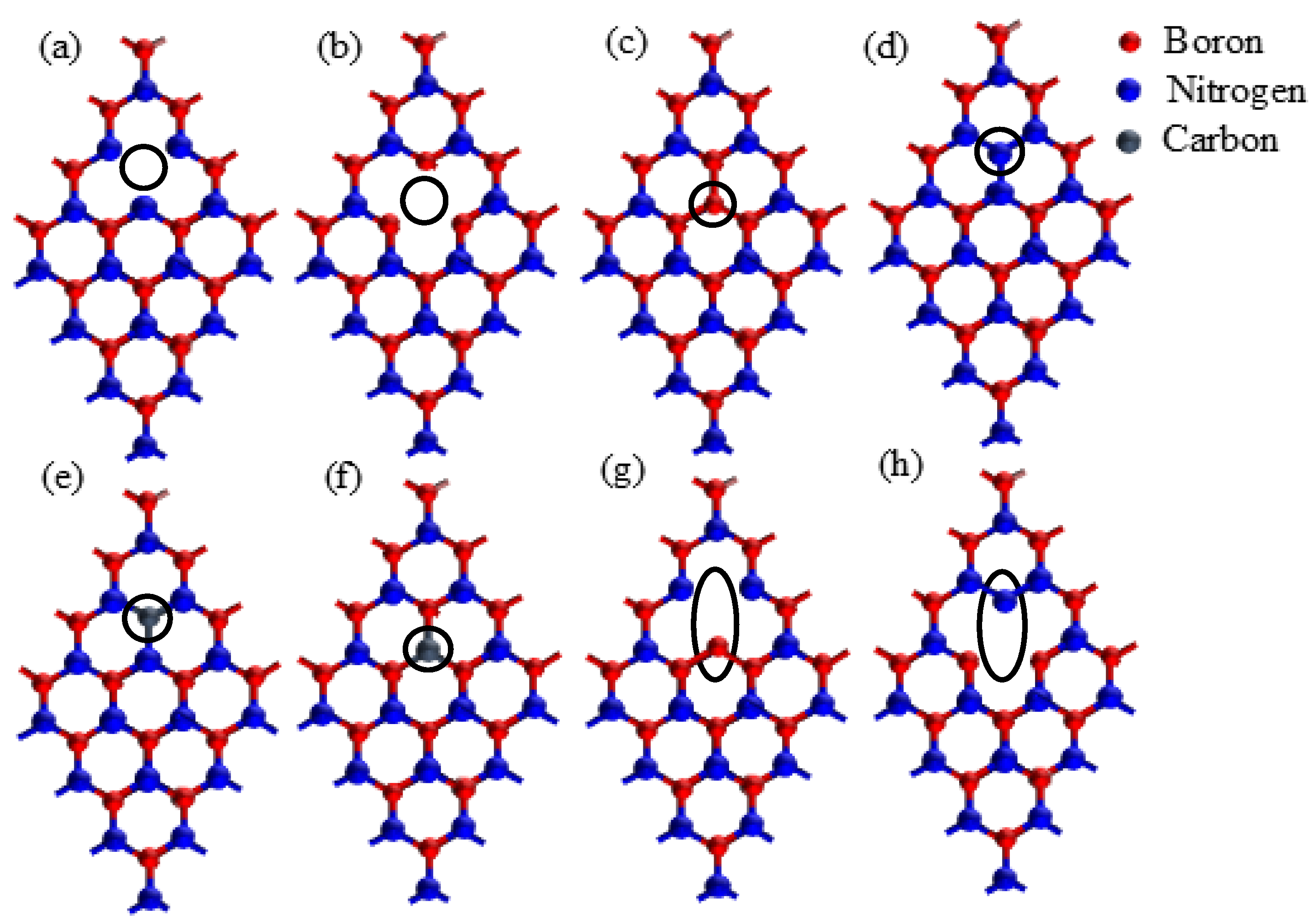
2. Materials and Methods
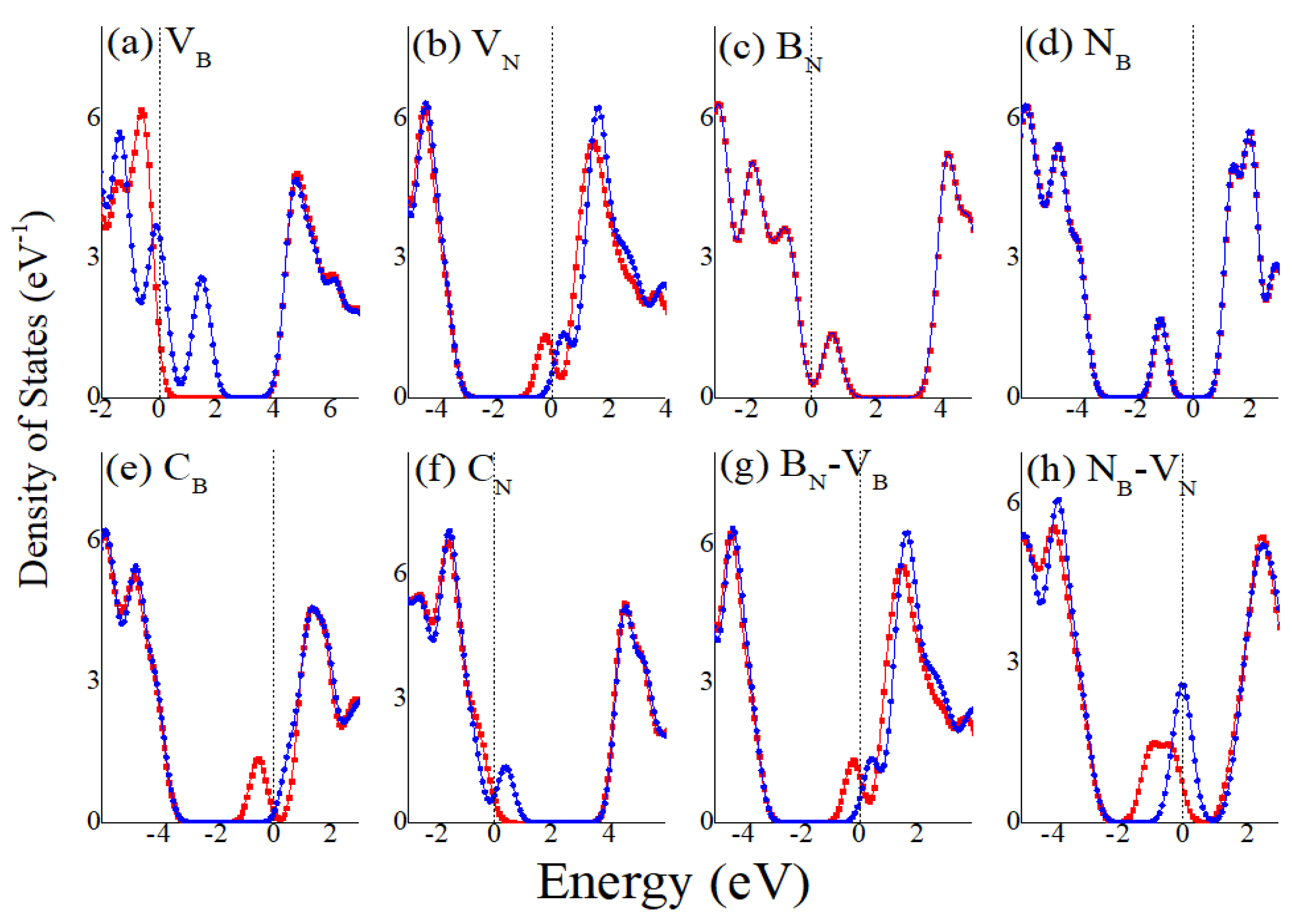
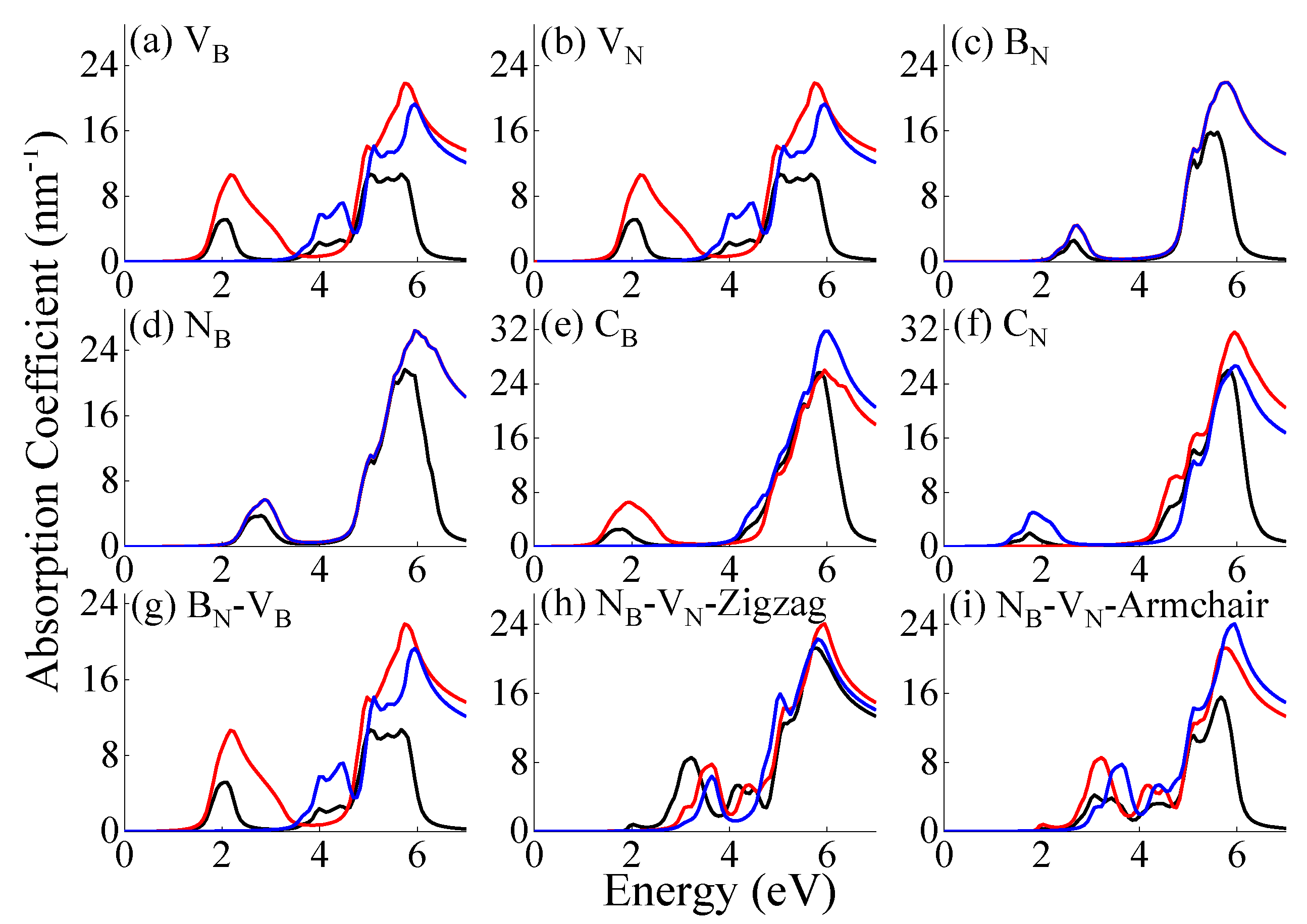
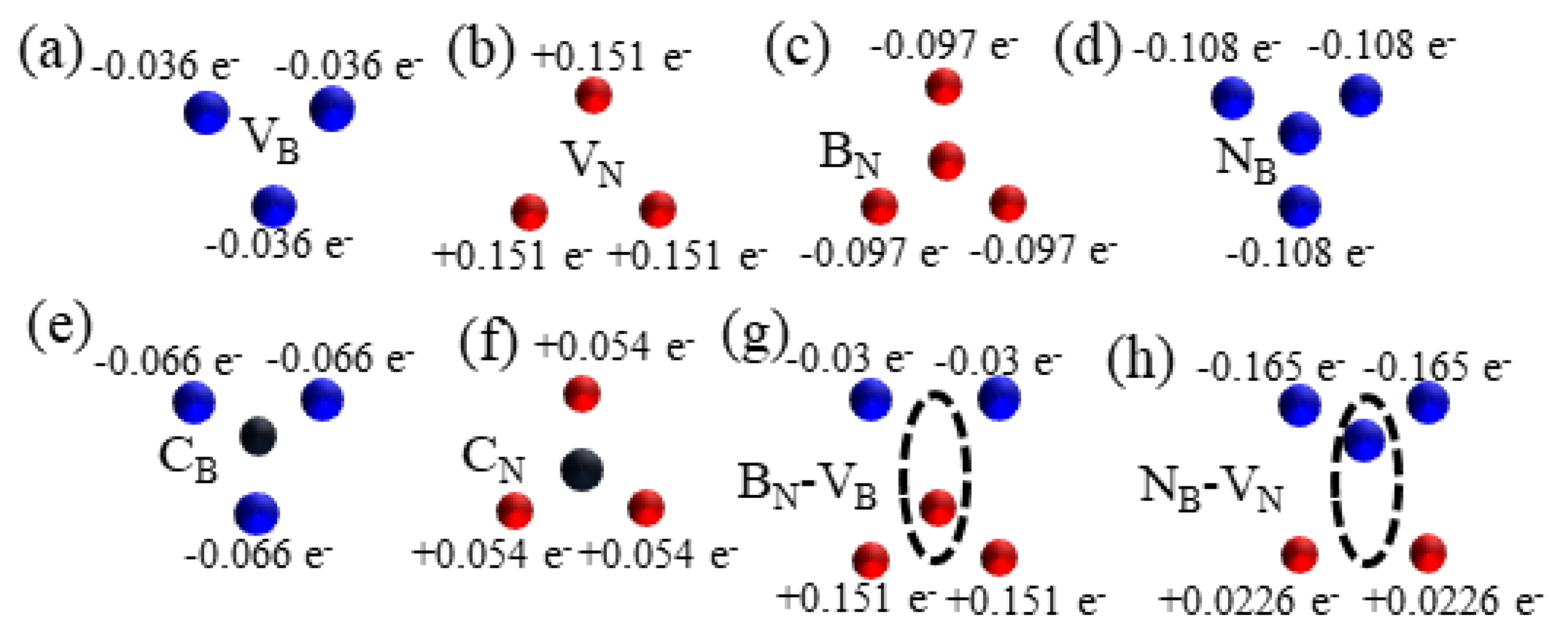
The Virtual Nanolab Atomistix ToolKit (ATK) package (QuantumATK 2018.06-SP1) with the density functional theory (DFT) was used for the first-principle calculation of the electronic and optical properties of the BN monolayer for the various point defects [52]. The Perdew–Burke–Ernzerhof (PBE) parametrization of the generalized gradient approximations (GGA) exchange-correlation with a double zeta polarized (DZP) basis was used with a mesh cut-off energy of 150 Ry [53]. The electron temperature was set to 300 K for the simulations of the band structure, density of states (DOS), and dielectric constant (ε) for the defects in the BN monolayer. A 11 × 11 × 1 Monkhorst–Pack k-grid mesh in this simulation was employed [54]. All atomic positions and lattice constants were optimized by using the generalized gradient approximations (GGA) with the maximum Hellmann–Feynman forces of 0.05 eV/Å, which was sufficient to obtain the relaxed structures [55,56]. The Pulay-mixer algorithm was employed as an iteration control parameter with a 105 tolerance value [57]. The maximum number of fully self-consistent field (SCF) iteration steps was set to 100 [58]. The periodic boundary conditions were employed for all three directions [59]. A separation of 60 Å for the adjacent layers was utilized to minimize the mirroring interaction. The self-consistent field calculations fully guaranteed the convergence within the iteration steps.
The hBN supercell consists of 4 × 4-unit cells with 16 boron atoms and 16 nitrogen atoms. Figure 1 shows the defects in a supercell including the boron vacancy (VB), nitrogen vacancy (VN), substitution of boron for nitrogen (BN), substitution of nitrogen for boron (NB), substitution of carbon for boron (CB), substitution of carbon for nitrogen (CN), substitution of boron for nitrogen with boron vacancy (BN-VB), and substitution of nitrogen for boron with nitrogen vacancy (NB-VN). The electronic band structure, density of states (DOS), and dielectric constant (ε) of the hBN supercell with various defects were characterized by the first principle calculation with density functional theory. The first principle calculation for electronic and optical properties of BN monolayer with atomic defects included the spin-orbit coupling (SOC). The spin-resolved absorption and reflection coefficients were calculated as a function of photon energy. Furthermore, the formation energy of hBN for various defects was studied to analyze the stability of each structure.

3. Results

Figure 2 displays the spin-resolved electronic band structure of the hBN monolayer with various defects. The energy levels were introduced within the forbidden band between the conduction band minimum (CBM) and the valence band maximum (VBM). The electronic band structure of the pristine BN monolayer displayed a direct bandgap of ~4.7 eV, which was located at the K-point in the first Brillouin Zone. The energy levels of electron spin-up and -down states for hBN with various defects were clearly resolved except for the hBN with the BN defect, where the energy levels degenerated. The Fermi energy level that was pinned to 0 eV fluctuated between the CBM and the VBM of an atomic layer with various defects. The atomic layer with the VB defect displayed hole-dominant characteristics due to the ascendant uncoupled holes around the boron vacancy [15], while the atomic layer with VN defect exhibited a donor-dominant characteristic due to the ascendant uncoupled electrons around the nitrogen-vacancy. Various defect-induced electronic characteristics in hBN including the energy levels in the forbidden gap, conduction and valence band, and Fermi level are shown in Figure 2a–h. The positively charged defect is the nitrogen vacancy, while the negatively charged defect is the boron vacancy. The charged defects shift the Fermi energy level in the band structure. In Figure 2a, the VB-defect in hBN induced the shallow energy levels from the conduction band. In Figure 2b, the VN-defect in hBN induced the deep energy levels from the conduction band. In Figure 2c,f, the positively charged defects of BN and CN induced the relatively shallow energy levels from the conduction band. In Figure 2d,e, the negatively charged defects of NB and CB induced the deep energy levels from the conduction band. In Figure 2g, BN-VB defects in hBN also induced the deep energy levels from the conduction band. In Figure 2h, the NB-VN defect in hBN introduced deep and shallow energy levels from the conduction band.
Figure 3 shows the spin-resolved electronic density of states (DOS) for the hBN monolayer with various defects. The vertical dashed line indicates the Fermi energy level, which is pinned to 0 eV. The abundant electronic DOS across the Fermi level were observed for the BN atomic layer with VB, CB, and NB-VN defects, which indicates the high conduction electronic characteristics. For the BN atomic layer with the BN defect, the spin up- and spin down-DOS overlapped each other, which led to zero spin-dipole magnetic moments. The atomic layer with defects of VN and BN-VB displayed a similar electronic band structure and DOS due to the structural instability with the BN-VB defect, where the boron substitution jumped to the neighboring vacancy position. The atomic layer with the BN-VB defect eventually transformed into an atomic layer with a VN-like defect during the structural optimization process. The BN-VB defect is unstable in the structure because a minimum total energy is required for the system to be stable. The defects of VB, VN, CN, BN-VB, and NB-VN in hBN induced the metallic characteristics. A point VB defect in a 4 × 4 unit cell offers a high defect density of 1.155 × 1014 cm−2. The strong doping with high defect density induces metallicity and shifts the Fermi level into the valence band. The metallicity with the defects of VN, CN, BN-VB, and NB-VN is attributable to the defect-induced large density of states around the Fermi energy level.
Figure 4 shows the with and without spin-resolved absorption spectra for the hBN supercell with various defects of (a) VB, (b) VN, (c) BN, (d) NB, (e) CB, (f) CN, (g) BN-VB, and (h) NB-VN in a zigzag direction, and (i) NB-VN in an armchair direction. In Figure 4, black, red, and blue lines indicate without spin-resolved, -up, and -down absorption spectra. The absorption peaks of hBN with defects were shifted in the visible spectral region. The mechanism of optical absorption in the lower energy regions is due to the electronic transitions from the conduction band to the defected-mediated energy band in the forbidden gap. Similarly, in the higher energy regions, it is due to the electronic transitions from the conduction band to the valence band. The absorption peak of spin-unresolved hBN with CN is shown at ~1.75 eV (Figure 4f), while that with NB defect is exhibited at ~2.8 eV (Figure 4d). The hBN with the NB-VN defect displays the anisotropic optical characteristics of distinct absorption and reflection coefficients along with the zigzag and armchair directions, which are shown in Figure 4h. The hBN with the NB-VN defect exhibits the unresolved absorption peaks at ~1.96 eV along the zigzag direction and ~3.01 eV and 3.34 eV along the armchair direction. The spin-resolved absorption coefficient shows that the spin-up electron has a relatively higher absorption coefficient than that of the spin-down electrons for the atomic layer with VB, VN, CB, and BN-VB defects, while the spin-up and -down electrons have almost equal absorption characteristics for the atomic layers with BN and NB defects. The spin-down electrons in the atomic layer with the CN defect have dominant absorption at ~1.75 eV. In addition, the effect of density functionals on the results of electronic properties and absorption coefficients is presented in Supplementary Materials. It was found that the hybrid methods, including B3LYP and PBE0 with higher HF exchange percentage, displayed a larger band gap and absorption blue shift.
Figure 5 shows the reflection coefficients as a function of photon energy for the hBN monolayer with the various defects of (a) VB, (b) VN, (c) BN, (d) NB, (e) CB, (f) CN, (g) BN-VB, and (h) NB-VN in a zigzag direction, and (i) NB-VN in an armchair direction. In Figure 5, black, red, and blue lines indicate the spin-unresolved (×10), -up, and -down reflection spectra. The spin-resolved reflection coefficients of the hBN atomic layer with the defect were one order larger than that of spin-unresolved electrons because the real part of the dielectric constant for the spin-resolved hBN atomic layer with defects is larger than that of spin-unresolved hBN atomic layer with defects. The hBN with the CN defect has the highest reflection peak at ~6.0 eV, whereas the hBN with the VB defect has the lowest peak at ~5.8 eV. It should be noteworthy that the hBN with the VB defect has two prominent reflection peaks at ~1.89 eV and ~2.10 eV. The hBN atomic layer with defects has minimal reflection coefficients from ~4.0 to 5.0 eV, which implies the existence of optical absorption through an optical bandgap. In analogy to the absorption spectra, the reflection spectra of hBN with BN and NB defects were overlapped with degeneracy for the spin-up and –down electrons.
The structural stability of the hBN monolayer with different defects was analyzed with the formation energy of the localized single defect within the supercell of 4 × 4 unit cells. Figure 6 displays the phonon band structure of the monolayer with the defects. It was found that only the hBN monolayer with the NB-VN defect demonstrated the imaginary vibrational mode that implies the structural instability.
In addition, the molecular orbitals of every atom one by one for each monolayer with various defects and the corresponding calculated charge transfers between the defects and their neighboring atoms were investigated by learning the orbital charge change during defect doping. Figure 7 shows the charge transfer of neighboring atoms around charged defects. The intrinsic charge of various defects in the hBN monolayer based on the information on defective charge transfer is listed in Table 1. It was found that the defects of VB, BN, NB, and CB are p-type doping, while all the other defects are n-type doping.
Furthermore, the charged point defect modified the optical spectra of the hBN monolayer. The VB defect is an acceptor-like defect because the Fermi level is shifted toward the VBM. The VN is a donor-like defect because the Fermi level is shifted toward the CBM. Therefore, the VB defect has an affinity with the negative charge of electron, and the VN defect has an affinity with the positive change of the hole. Figure 8 displays the absorption and reflection coefficients of hBN atomic layer with the charged defects of VB for VB −1, VB−2, and VB−3 and VN for VN+1, VN+2, and VN+3. In Figure 8 c, the hBN with positively charged defects of VN+1, VN+2, and VN+3 displayed optical absorption characteristics at the shorter and longer energy spectral regions. According to Figure 2b, the VN-defect induced deep energy levels from the conduction band. The optical absorption in the lower energy spectral regions for the positively charged defects is attributable to the electronic transition from the conduction band to the defect-mediated energy states in the forbidden gap. Similarly, in the longer energy spectra, the optical absorption is attributable to the electronic transition from the conduction to the valence band. The negatively charged VB-defect in hBN induced the shallow energy levels from the conduction band, which is shown in Figure 2a. This implies that the optical absorption at the lower and the higher energy spectral regions for the negatively charged defects shown in Figure 8a are attributable to electronic transition from the deep/shallow conduction band to the defect-induced energy states in the forbidden gap, and the transition from the conduction to the valence band, respectively. In Figure 8b, the hBN with negatively charged defects of VB−1 and VB−2 have visible reflection characteristics, but the hBN with VB−3 does not display the visible reflection characteristics. Figure 8d shows the reflection spectral characteristics for the charge defects VN+1, VN+2, and VN+3 in hBN supercells. These defects in hBN display the characteristic reflection spectra at the lower energy spectral region. The reflection spectra of charge defects of VN+2 and VN+3 in the hBN supercells display a weak discrepancy at the lower energy spectral region. The reflection coefficients due to the charged defect of VN+1 in the hBN supercell are close to zero at the lower energy spectral region, which is a distinct spectral characteristic from the reflection spectra of VN+2 and VN+3 in hBN supercells. However, the spectra of charge defects VN+1, VN+2, and VN+3 in the hBN supercells at the higher energy spectral region do not exhibit apparent visual differences with the graphical scale of reflection coefficients. The experimental photoluminescence excitation (PLE) measurement of an ensemble of negatively charged VB defects with a broad excitation range from 1.8 eV to 3.0 eV for the PL at 2.6 eV [27] has been reported, which is evidenced by the theoretical prediction in Figure 8a.
The effective modulations of electronic and optical properties of hBN monolayers with various atomic defects and different doping concentrations will also advance optoelectronics applications. A high concentration of defects over ~1013/cm2 has been experimentally realized by nitrogen cluster doping in graphene [60] and the plasma-assisted method for WS2 monolayers [61]. In addition, electrostatic doping induces deep doping in 2D materials. For instance, the carrier doping densities have been experimentally obtained up to ~1013/cm2 in the 2D transition metal dichalcogenide (MoS2 and WSe2) monolayers [38,39] and up to ~1014/cm2 in atomically thin Fe3GeTe2 [20] by back-gate gating, and up to ~1014/cm2 in graphene by the ion liquid gating [40,41]. Theoretical studies on the electronic and optical modulations of hBN for various atomic defects and different concentrations provides a plethora of information for prospective applications.

4. Conclusions

First-principle calculations with density functional theory characterized the visible optical spectra of the hBN monolayer with various point defects. The hBN supercells with VB, CB, and NB-VN defects exhibited a high electron density of states across the Fermi level, which indicates highly conductive electronic characteristics. The hBN atomic layer with NB-VN defects displayed anisotropic optical and electronic characteristics along the armchair and zigzag directions. The hBN atomic layer with defects, except for the antisite, of boron and nitrogen displayed spin-resolved optical absorption within the forbidden gap. The hBN with positively charged defects showed dominant optical and electronic characteristics at the longer spectral region. The spin-resolved visible optical and electronic characteristics of defect-mediated hBN atomic layers will promote the exploitation of 2D optoelectronics.

Supplementary Materials

The following supporting information can be downloaded at: https://www.mdpi.com/article/10.3390/cryst12070906/s1. The effect of density functionals on the results of electronic properties and absorption coefficients.

Author Contributions

Conceptualization, F.J.S.; methodology, S.Y., Q.L., and T.N.; formal analysis, S.Y. and T.N.; resources, F.J.S.; writing—original draft preparation, S.Y.; writing—review and editing, F.J.S., B.T., T.N., and Q.L.; visualization, S.Y.; supervision, F.J.S. and B.T.; funding acquisition, F.J.S. All authors have read and agreed to the published version of the manuscript.

Funding

The research at HU was funded by ARO W911NF-15-1-0535, NSF HRD-1137747, and NASA NNX15AQ03A.

Conflicts of Interest

The authors declare no conflict of interest.

References

  1. Tsay, Y.F.; Vaidyanathan, A.; Mitra, S.S. Electronic structure and optical properties of cubic BN. Phys. Rev. B 1979, 19, 5422. [Google Scholar] [CrossRef]
  2. Larach, S.; Shrader, R.E. Electroluminescence from Boron Nitride. Phys. Rev. 1956, 102, 582. [Google Scholar] [CrossRef]
  3. Johnson, Q.; Mitchell, A.C. First X-ray Diffraction Evidence for a Phase Transition during Shock-Wave Compression. Phys. Rev. Lett. 1972, 29, 1369. [Google Scholar] [CrossRef]
  4. Gielisse, P.J.; Mitra, S.S.; Plendl, J.N.; Griffis, R.D.; Mansur, L.C.; Marshall, R.; Pascoe, E.A. Lattice Infrared Spectra of Boron Nitride and Boron Monophosphide. Phys. Rev. 1967, 155, 1039. [Google Scholar] [CrossRef]
  5. Kleinman, L.; Phillips, J.C. Crystal Potential and Energy Bands of Semiconductors. II. Self-Consistent Calculations for Cubic Boron Nitride. Phys. Rev. 1960, 117, 460. [Google Scholar] [CrossRef]
  6. Yu, S.; Tabibi, B.; Li, Q.; Seo, F.J. Piezoelectric enhancement of a defect-mediated boron nitride nanotube. J. Phys. D Appl. Phys. 2019, 52, 335304. [Google Scholar] [CrossRef]
  7. Watanabe, K.; Taniguchi, T.; Kanda, H. Direct-bandgap properties and evidence for ultraviolet lasing of hexagonal boron nitride single crystal. Nat. Mater. 2004, 3, 404–409. [Google Scholar] [CrossRef]
  8. Guo, H.; Gao, J.; Ishida, N.; Xu, M.; Fujita, D. Characterization of two-dimensional hexagonal boron nitride using scanning electron and scanning helium ion microscopy. Appl. Phys. Lett. 2014, 104, 031607. [Google Scholar] [CrossRef]
  9. Arnaud, B.; Lebègue, S.; Rabiller, P.; Alouani, M. Huge Excitonic Effects in Layered Hexagonal Boron Nitride. Phys. Rev. Lett. 2006, 96, 026402. [Google Scholar] [CrossRef] [Green Version]
  10. Jin, C.; Lin, F.; Suenaga, K.; Iijima, S. Fabrication of a Freestanding Boron Nitride Single Layer and Its Defect Assignments. Phys. Rev. Lett. 2009, 102, 195505. [Google Scholar] [CrossRef] [Green Version]
  11. Kubota, Y.; Watanabe, K.; Tsuda, O.; Taniguchi, T. Deep Ultraviolet Light-Emitting Hexagonal Boron Nitride Synthesized at Atmospheric Pressure. Science 2007, 317, 932–934. [Google Scholar] [CrossRef] [PubMed] [Green Version]
  12. Jiang, J.; Liang, Q.; Meng, R.; Yang, Q.; Tan, C.; Sunab, X.; Chen, X. Exploration of new ferromagnetic, semiconducting, and biocompatible Nb3X8 (X = Cl, Br or I) monolayers with considerable visible and infrared light absorption. Nanoscale 2017, 9, 2992–3001. [Google Scholar] [CrossRef] [PubMed]
  13. Yang, Q.; Zhang, S.; Tan, C.; Ye, H.; Ming, X.; Ingebrandt, S.; Chen, X. Considering the spin–orbit coupling effect on the photocatalytic performance of AlN/MX2 nanocomposites. J. Mater. Chem. C 2017, 5, 9412–9420. [Google Scholar] [CrossRef]
  14. Yu, S.; Xiong, H.D.; Eshun, K.; Yuan, H.; Li, Q. Phase transition, effective mass, and carrier mobility of MoS2 monolayer under tensile strain. Appl. Surf. Sci. 2015, 325, 27–32. [Google Scholar] [CrossRef]
  15. Yu, S.; Zhu, H.; Eshun, K.; Shi, C.; Zeng, M.; Li, Q. Strain-engineering the anisotropic electrical conductance in ReS2 monolayer. Appl. Phys. Lett. 2016, 108, 191901. [Google Scholar] [CrossRef]
  16. Eshun, K.; Xiong, H.D.; Yu, S.; Li, Q. Doping induces large variation in the electrical properties of MoS2 monolayers. Solid-State Electron. 2015, 106, 44–49. [Google Scholar] [CrossRef]
  17. Zhang, Z.; Guo, W. Energy-gap modulation of BN ribbons by transverse electric fields: First-principles calculations. Phys. Rev. B 2008, 77, 075403. [Google Scholar] [CrossRef] [Green Version]
  18. Zhang, Z.; Guo, W. Tunable Ferromagnetic Spin Ordering in Boron Nitride Nanotubes with Topological Fluorine Adsorption. J. Am. Chem. Soc. 2009, 131, 6874–6879. [Google Scholar] [CrossRef]
  19. Zhang, Z.; Guo, W.; Yakobson, B.I. Self-modulated band gap in boron nitride nanoribbons and hydrogenated sheets. Nanoscale 2013, 5, 6381–6387. [Google Scholar] [CrossRef] [Green Version]
  20. Wang, V.; Ma, N.; Mizuseki, H.; Kawazoe, Y. First-principles study of intrinsic defect properties in hexagonal BN bilayer and monolayer. Solid State Commun. 2012, 152, 816–820. [Google Scholar] [CrossRef]
  21. Hou, S.; Birowosuto, M.D.; Umar, S.; Anicet, M.A.; Tay, R.Y.; Coquet, P.; Tay, B.K.; Wang, H.; Teo, E.H.T. Localized emission from laser-irradiated defects in 2D hexagonal boron nitride. 2D Mater. 2018, 5, 015010. [Google Scholar] [CrossRef]
  22. Auwärter, W.; Muntwiler, M.; Osterwalder, J.; Greber, T. Defect lines and two-domain structure of hexagonal boron nitride films on Ni(1 1 1). Surf. Sci. 2003, 545, L735–L740. [Google Scholar] [CrossRef]
  23. Wong, D.; Velasco, J., Jr.; Ju, L.; Lee, J.; Kahn, S.; Tsai, H.; Germany, C.; Taniguchi, T.; Watanabe, K.; Zettl, A.; et al. Characterization and manipulation of individual defects in insulating hexagonal boron nitride using scanning tunnelling microscopy. Nat. Nanotechnol. 2015, 10, 949–953. [Google Scholar] [CrossRef]
  24. Tran, T.T.; Bray, K.; Ford, M.J.; Toth, M.; Aharonovich, I. Quantum emission from hexagonal boron nitride monolayers. Nat. Nanotechnol. 2016, 11, 37–41. [Google Scholar] [CrossRef] [PubMed]
  25. Exarhos, A.L.; Hopper, D.A.; Grote, R.R.; Alkauskas, A.; Bassett, L.C. Optical Signatures of Quantum Emitters in Suspended Hexagonal Boron Nitride. ACS Nano 2017, 11, 3328–3336. [Google Scholar] [CrossRef] [PubMed] [Green Version]
  26. Grosso, G.; Moon, H.; Lienhard, B.; Ali, S.; Efetov, D.K.; Furchi, M.M.; Jarillo-Herrero, P.; Ford, M.J.; Aharonovich, I.; Englund, D. Tunable and high-purity room temperature single-photon emission from atomic defects in hexagonal boron nitride. Nat. Commun. 2017, 8, 705. [Google Scholar] [CrossRef]
  27. Kianinia, M.; Fröch, S.W.J.E.; Bradac, C.; Aharonovich, I. Generation of Spin Defects in Hexagonal Boron Nitride. ACS Photonics 2020, 7, 2147–2152. [Google Scholar] [CrossRef]
  28. Xu, Z.Q.; Elbadawi, C.; Tran, T.T.; Kianinia, M.; Li, X.; Liu, D.; Hoffman, T.B.; Nguyen, M.; Kim, S.; Edgar, J.H.; et al. Single photon emission from plasma treated 2D hexagonal boron nitride. Nanoscale 2018, 10, 7957–7965. [Google Scholar] [CrossRef] [Green Version]
  29. Mendelson, N.; Chugh, D.; Reimers, J.R.; Cheng, T.S.; Gottscholl, A.; Long, H.; Mellor, C.J.; Zettl, A.; Dyakonov, V.; Beton, P.H.; et al. Identifying carbon as the source of visible single-photon emission from hexagonal boron nitride. Nat. Mater. 2021, 20, 321–328. [Google Scholar] [CrossRef]
  30. Sajid, A.; Thygesen, K.S. VNCB defect as source of single photon emission from hexagonal boron nitride. 2D Mater. 2020, 7, 031007. [Google Scholar] [CrossRef]
  31. Turiansky, M.E.; Alkauskas, A.; Bassett, L.C.; Walle, C.G.V. Dangling Bonds in Hexagonal Boron Nitride as Single-Photon Emitters. Phys. Rev. Lett. 2019, 123, 127401. [Google Scholar] [CrossRef] [PubMed] [Green Version]
  32. Mendelson, N.; Xu, Z.Q.; Tran, T.T.; Kianinia, M.; Scott, J.; Bradac, C.; Aharonovich, I.; Toth, M. Engineering and Tuning of Quantum Emitters in Few-Layer Hexagonal Boron Nitride. ACS Nano 2019, 13, 3132–3140. [Google Scholar] [CrossRef] [PubMed]
  33. Roondhe, B.; Jha, P.K.; Ahuja, R. Haeckelite boron nitride as nano sensor for the detection of hazardous methyl mercury. Appl. Surf. Sci. 2020, 506, 144860. [Google Scholar] [CrossRef]
  34. Cheng, C.; Li, Z.; Dong, N.; Li, R.; Wang, J.; Chen, F. Atomic Defect Induced Saturable Absorption of Hexagonal Boron Nitride in Near Infrared Band for Ultrafast Lasing Applications. Nanomaterials 2021, 11, 3203. [Google Scholar] [CrossRef] [PubMed]
  35. Hamdi, H.; Thiering, G.; Bodrog, Z.; Ivady, V.; Gali, A. Stone–Wales defects in hexagonal boron nitride as ultraviolet emitters. npj Comput. Mater. 2020, 6, 178. [Google Scholar] [CrossRef]
  36. Ding, Y.; Davila, F.T.; Khatar, A.; Nash, D.; Blair, R.; Tetard, L. Defect engineering in Boron Nitride for catalysis. MRS Commun. 2018, 8, 1236–1243. [Google Scholar] [CrossRef]
  37. Azevedo, S.; Kaschny, J.R.; de Castilho, C.M.C.; de Brito Mota, F. Electronic structure of defects in a boron nitride monolayer. Eur. Phys. J. B 2009, 67, 507–512. [Google Scholar] [CrossRef]
  38. Attaccalite, C.; Wirtz, L.; Marini, A.; Rubio, A. Efficient Gate-tunable light-emitting device made of defective boron nitride nanotubes: From ultraviolet to the visible. Sci. Rep. 2013, 3, 2698. [Google Scholar] [CrossRef] [Green Version]
  39. Topsakal, M.; Aktürk, E.; Ciraci, S. First-principles study of two- and one-dimensional honeycomb structures of boron nitride. Phys. Rev. B 2009, 79, 115442. [Google Scholar] [CrossRef]
  40. Grinyaev, S.N.; Konusov, F.V.; Lopatin, V.V.; Shiyan, L.N. Optical absorption of hexagonal boron nitride involving nitrogen vacancies and their complexes. Phys. Solid State 2004, 46, 435–441. [Google Scholar] [CrossRef]
  41. Kim, D.H.; Kim, H.S.; Song, M.W.; Lee, S.; Lee, S.Y. Geometric and electronic structures of monolayer hexagonal boron nitride with multi-vacancy. Nano Converg. 2017, 4, 13. [Google Scholar] [CrossRef] [PubMed]
  42. Sajid, A.; Reimers, J.R.; Ford, M.J. Defect states in hexagonal boron nitride: Assignments of observed properties and prediction of properties relevant to quantum computation. Phys. Rev. B 2018, 97, 064101. [Google Scholar] [CrossRef] [Green Version]
  43. Huang, B.; Lee, H. Defect and impurity properties of hexagonal boron nitride: A first-principles calculation. Phys. Rev. B 2012, 86, 245406. [Google Scholar] [CrossRef]
  44. Azevedo, S.; Kaschny, J.R.; De Castilho, C.M.C.; De Brito Mota, F. A theoretical investigation of defects in a boron nitride monolayer. Nanotechnology 2007, 18, 495707. [Google Scholar] [CrossRef] [PubMed]
  45. Reimers, J.R.; Sajid, A.; Kobayashi, R.; Ford, M.J. Understanding and Calibrating Density-Functional-Theory Calculations Describing the Energy and Spectroscopy of Defect Sites in Hexagonal Boron Nitride. J. Chem. Theory Comput. 2018, 14, 1602. [Google Scholar] [CrossRef] [PubMed]
  46. Tawfik, S.A.; Ali, S.; Fronzi, M.; Kianinia, M.; Tran, T.T.; Stampfl, C.; Aharonovich, I.; Toth, M.; Ford, M.J. First-principles investigation of quantum emission from hBN defects. Nanoscale 2017, 9, 13575–13582. [Google Scholar] [CrossRef] [PubMed] [Green Version]
  47. Wang, R.; Yang, J.; Wu, X.; Wang, S. Local charge states in hexagonal boron nitride with Stone–Wales defects. Nanoscale 2016, 8, 8210–8219. [Google Scholar] [CrossRef]
  48. Slotman, G.J.; Fasolino, A. Structure, stability and defects of single layer hexagonal BN in comparison to graphene. J Phys. Condens. Matter 2012, 25, 45009. [Google Scholar] [CrossRef] [Green Version]
  49. Wen, X.S.; Jian, C.; Jun, Z. Self-Healing of Stone–Wales Defects in Boron Nitride Monolayer by Irradiation: Ab Initio Molecular Dynamics Simulations. Chin. Phys. Lett. 2013, 30, 103102. [Google Scholar]
  50. Ansari, N.; Nazari, F.; Illas, F. Line defects and induced doping effects in graphene, hexagonal boron nitride and hybrid BNC. Phys. Chem. Chem. Phys. 2014, 16, 21473–21485. [Google Scholar] [CrossRef]
  51. Pham, T.; Gibb, A.L.; Li, Z.; Gilbert, S.M.; Song, C.; Louie, S.G.; Zettl, A. Formation and Dynamics of Electron-Irradiation-Induced Defects in Hexagonal Boron Nitride at Elevated Temperatures. Nano Lett. 2016, 16, 7142–7147. [Google Scholar] [CrossRef] [PubMed]
  52. Brandbyge, M.; Mozos, J.L.; Ordejón, P.; Taylor, J.; Stokbro, K. Density-functional method for nonequilibrium electron transport. Phys. Rev. B 2002, 65, 165401. [Google Scholar] [CrossRef] [Green Version]
  53. Sarkar, D.; Xie, X.; Liu, W.; Cao, W.; Kang, J.; Gong, Y.; Kraemer, S.; Ajayan, P.M.; Banerjee, K. A subthermionic tunnel field-effect transistor with an atomically thin channel. Nature 2015, 526, 91–95. [Google Scholar] [CrossRef]
  54. Monkhorst, H.J.; Pack, J.D. Special points for Brillouin-zone integrations. Phys. Rev. B 1976, 13, 5188. [Google Scholar] [CrossRef]
  55. Perdew, J.P.; Burke, K.; Ernzerhof, M. Generalized Gradient Approximation Made Simple. Phys. Rev. Lett. 1996, 77, 3865. [Google Scholar] [CrossRef] [Green Version]
  56. Yu, S.; Rice, Q.; Neupane, T.; Tabibi, B.; Li, Q.; Seo, F.J. Piezoelectricity enhancement and bandstructure modification of atomic defect mediated MoS2 monolayer. Phys. Chem. Chem. Phys. 2017, 19, 24271–24275. [Google Scholar] [CrossRef] [PubMed]
  57. Grimme, S. Semiempirical hybrid density functional with perturbative second-order correlation. J. Chem. Phys. 2006, 124, 034108. [Google Scholar] [CrossRef] [Green Version]
  58. Kohn, W.; Sham, L.J. Self-Consistent Equations Including Exchange and Correlation Effects. Phys. Rev. 1965, 140, A1133. [Google Scholar] [CrossRef] [Green Version]
  59. Makov, G.; Payne, M.C. Periodic boundary conditions in ab initio calculations. Phys. Rev. B 1995, 51, 4014. [Google Scholar] [CrossRef] [Green Version]
  60. Lin, L.; Li, J.; Yuan, Q.; Li, Q.; Zhang, J.; Sun, L.; Rui, D.; Chen, Z.; Jia, K.; Liu, Z. Nitrogen cluster doping for high-mobility/conductivity graphene films with millimeter-sized domains. Sci. Adv. 2019, 5, 8337. [Google Scholar] [CrossRef] [Green Version]
  61. Zhang, F.; Lu, Y.; Schulman, D.S.; Zhang, T.; Fujisawa, K.; Lin, Z.; Lei, Y.; Elias, A.L.; Das, S.; Sinnott, S.B.; et al. Carbon doping of WS2 monolayers: Bandgap reduction and p-type doping transport. Sci. Adv. 2019, 5, 5003. [Google Scholar] [CrossRef] [PubMed] [Green Version]
Figure 1. Schematic drawing of hBN monolayer supercells with various defects of (a) boron vacancy (VB), (b) nitrogen vacancy (VN), (c) substitution of boron for nitrogen (BN), (d) substitution of nitrogen for boron (NB), (e) substitution of carbon for boron (CB), (f) substitution of carbon for nitrogen (CN), (g) substitution of boron nitrogen and boron vacancy (BN-VB), and (h) substitution of nitrogen for boron with nitrogen vacancy (NB-VN).
Crystals 12 00906 g001
Figure 2. Spin-resolved electronic band structure of hBN monolayer with various defects of (a) VB; (b) VN; (c) BN; (d) NB; (e) CB; (f) CN; (g) BN-VB; and (h) NB-VN. The Fermi energy level is pinned to 0 eV. The red and blue lines indicate the spin-up and -down electronic band and energy levels.
Crystals 12 00906 g002
Figure 3. Spin-resolved electronic density of states (DOS) of hBN monolayer with various defects of (a) VB; (b) VN; (c) BN; (d) NB; (e) CB; (f) CN; (g) BN-VB; and (h) NB-VN. The vertical dotted lines indicate the Fermi energy level, which is pinned to 0 eV. The red and blue lines indicate the spin-up and -down DOS.
Crystals 12 00906 g003
Figure 4. Spin-resolved and -unresolved absorption spectra for the hBN supercell with various defects of (a) VB, (b) VN, (c) BN, (d) NB, (e) CB, (f) CN, (g) BN-VB, and (h) NB-VN in a zigzag direction, and (i) NB-VN in an armchair direction. The black, red, and blue lines indicate the spin-unresolved, -up, and -down absorption spectra.
Crystals 12 00906 g004
Figure 5. Reflection spectra of hBN supercell with the various defects of (a) VB, (b) VN, (c) BN, (d) NB, (e) CB, (f) CN, (g) BN-VB, and (h) NB-VN in a zigzag direction, and (i) NB-VN in an armchair direction. The black, red, and blue lines indicate the spin-unresolved (×10), -up, and -down reflection spectra.
Crystals 12 00906 g005
Figure 6. Phonon band structure of hBN monolayer with different defects. (a) VB, (b) VN, (c) BN, (d) NB, (e) CB, (f) CN, (g) BN-VB, and (h) NB-VN.
Crystals 12 00906 g006
Figure 7. Charge transfer of neighboring atoms around charged defects. ‘+’ and ‘−’ denote absorbing and losing electrons during doping, respectively. (a) VB, (b) VN, (c) BN, (d) NB, (e) CB, (f) CN, (g) BN-VB, and (h) NB-VN.
Crystals 12 00906 g007
Figure 8. Optical spectra of hBN monolayer with charged defects. (a) Absorption and (b) reflection spectra of hBN supercell with various charged defects of VB −1, VB−2, and VB−3 (c) absorption and (d) reflection spectra of hBN supercell with various charged defects of VN+1, VN+2, and VN+3.
Crystals 12 00906 g008
Table 1. Intrinsic charge of various defects in hBN monolayer.
DefectsVBVNBNNBCBCNBN-VBNB-VN
Intrinsic charge (e)−0.108+0.453−0.291−0.324−0.192+0.162+0.242+0.122
Publisher’s Note: MDPI stays neutral with regard to jurisdictional claims in published maps and institutional affiliations.

