
Piezoresistive Memories Based on Two-Dimensional Nano-Scale Electromechanical Systems


Abstract
:1. Introduction
2. Methods
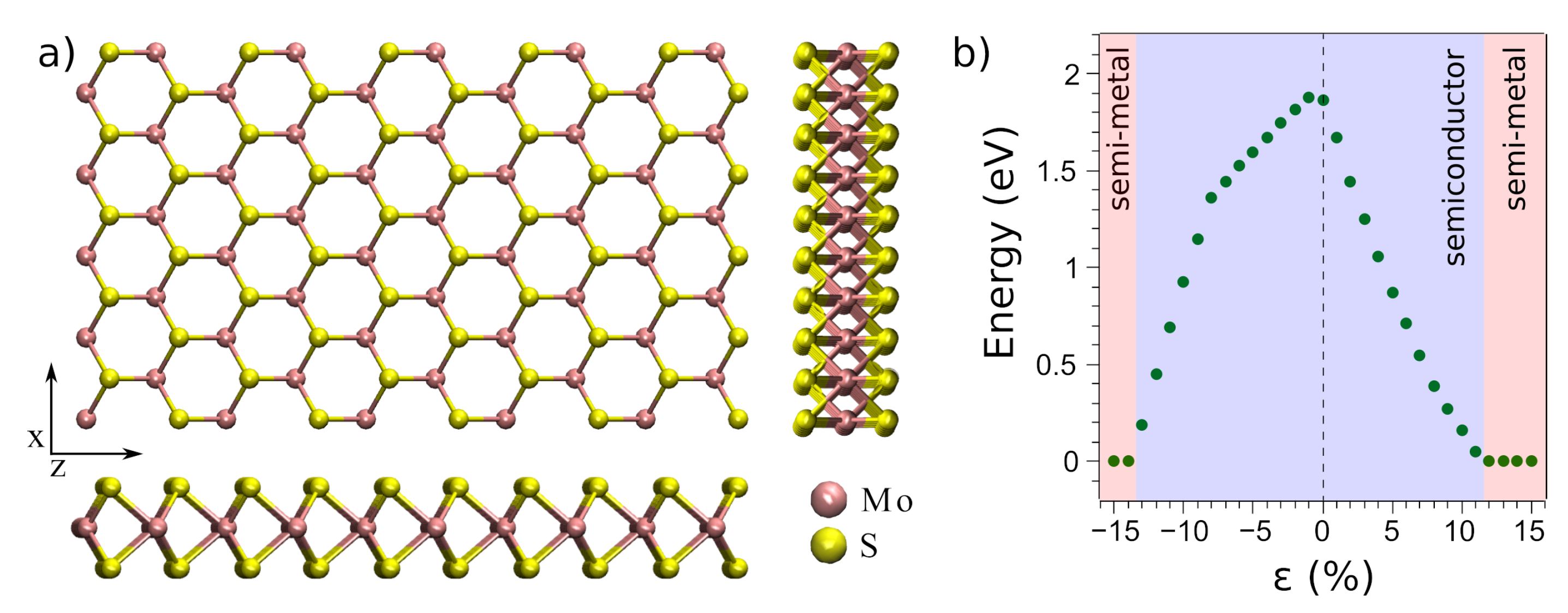
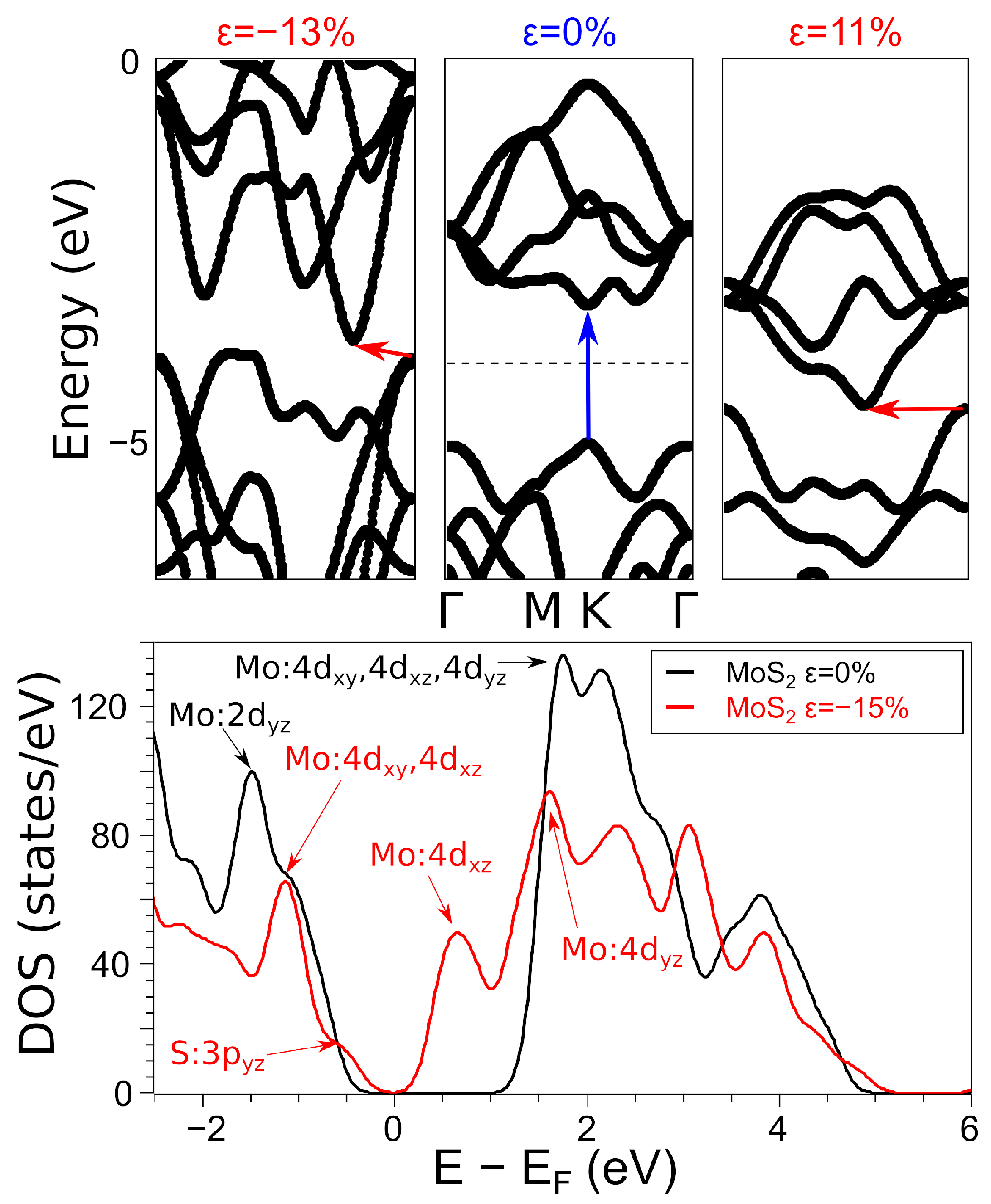
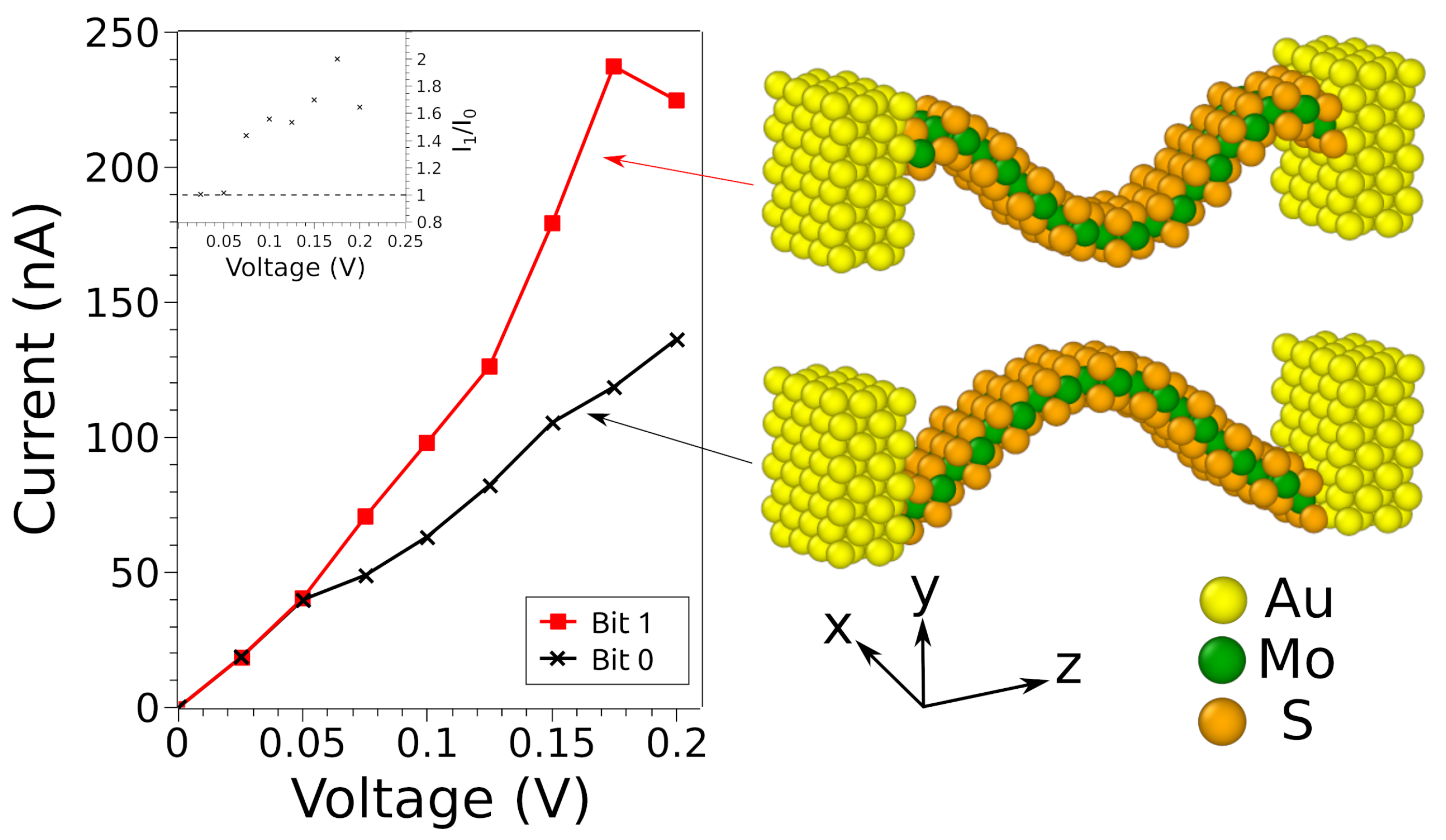
3. Results
3.1. Vertical 2D Heterostructure
3.2. Asymmetries on Clamping
4. Conclusions
Author Contributions
Funding
Data Availability Statement
Conflicts of Interest
References
- Lee, J.S.; Lee, S.; Noh, T.W. Resistive switching phenomena: A review of statistical physics approaches. Appl. Phys. Rev. 2015, 2, 031303. [Google Scholar] [CrossRef] [Green Version]
- Jeong, D.S.; Thomas, R.; Katiyar, R.; Scott, J.; Kohlstedt, H.; Petraru, A.; Hwang, C.S. Emerging memories: Resistive switching mechanisms and current status. Rep. Prog. Phys. 2012, 75, 076502. [Google Scholar] [CrossRef] [PubMed]
- Ye, C.; Wu, J.; He, G.; Zhang, J.; Deng, T.; He, P.; Wang, H. Physical mechanism and performance factors of metal oxide based resistive switching memory: A review. J. Mater. Sci. Technol. 2016, 32, 1–11. [Google Scholar] [CrossRef]
- Wang, H.; Yan, X. Overview of resistive random access memory (RRAM): Materials, filament mechanisms, performance optimization, and prospects. Phys. Status Solidi (RRL)-Res. Lett. 2019, 13, 1900073. [Google Scholar] [CrossRef]
- Russo, U.; Ielmini, D.; Cagli, C.; Lacaita, A.L. Filament conduction and reset mechanism in NiO-based resistive-switching memory (RRAM) devices. IEEE Trans. Electron Devices 2009, 56, 186–192. [Google Scholar] [CrossRef]
- Akinaga, H.; Shima, H. Resistive random access memory (ReRAM) based on metal oxides. Proc. IEEE 2010, 98, 2237–2251. [Google Scholar] [CrossRef]
- Wong, H.S.P.; Lee, H.Y.; Yu, S.; Chen, Y.S.; Wu, Y.; Chen, P.S.; Lee, B.; Chen, F.T.; Tsai, M.J. Metal–oxide RRAM. Proc. IEEE 2012, 100, 1951–1970. [Google Scholar] [CrossRef]
- Carlos, E.; Branquinho, R.; Martins, R.; Kiazadeh, A.; Fortunato, E. Recent Progress in Solution-Based Metal Oxide Resistive Switching Devices. Adv. Mater. 2021, 33, 2004328. [Google Scholar] [CrossRef] [PubMed]
- Lata, L.K.; Jain, P.K.; Jain, A.; Bhatia, D. An Overview of Current Trends in Hafnium Oxide–Based Resistive Memory Devices. In Nanotechnology; CRC Press: Boca Raton, FL, USA, 2022; pp. 1–18. [Google Scholar]
- Kim, H.D.; An, H.M.; Lee, E.B.; Kim, T.G. Stable bipolar resistive switching characteristics and resistive switching mechanisms observed in aluminum nitride-based ReRAM devices. IEEE Trans. Electron Devices 2011, 58, 3566–3573. [Google Scholar] [CrossRef]
- Kim, M.J.; Jeon, D.S.; Park, J.H.; Kim, T.G. Bipolar resistive switching characteristics in tantalum nitride-based resistive random access memory devices. Appl. Phys. Lett. 2015, 106, 203101. [Google Scholar] [CrossRef]
- Carbone, M. NiO-Based Electronic Flexible Devices. Appl. Sci. 2022, 12, 2839. [Google Scholar] [CrossRef]
- Kim, Y.; Min, Y.; Lee, J.; Sohn, H. Ovonic Threshold Switching Selection Device Based on Chalcogenide ZnTe for Cross-Point ReRAM Device. In ECS Meeting Abstracts; IOP Publishing: Bristol, UK, 2014; p. 2048. [Google Scholar]
- Nam, K.H.; Kim, J.H.; Cho, W.J.; Kim, C.H.; Chung, H.B. Resistive switching in amorphous GeSe-based resistive random access memory. J. Nanosci. Nanotechnol. 2016, 16, 10393–10396. [Google Scholar] [CrossRef]
- Tranchant, J.; Pellaroque, A.; Janod, E.; Angleraud, B.; Corraze, B.; Cario, L.; Besland, M.P. Deposition of GaV4S8 thin films by H2S/Ar reactive sputtering for ReRAM applications. J. Phys. D Appl. Phys. 2014, 47, 065309. [Google Scholar] [CrossRef]
- Bai, W.; Huang, R.; Cai, Y.; Tang, Y.; Zhang, X.; Wang, Y. Record low-power organic RRAM with sub-20-nA reset current. IEEE Electron Device Lett. 2013, 34, 223–225. [Google Scholar] [CrossRef]
- Mu, B.; Hsu, H.H.; Kuo, C.C.; Han, S.T.; Zhou, Y. Organic small molecule-based RRAM for data storage and neuromorphic computing. J. Mater. Chem. C 2020, 8, 12714–12738. [Google Scholar] [CrossRef]
- Cai, Y.; Tan, J.; YeFan, L.; Lin, M.; Huang, R. A flexible organic resistance memory device for wearable biomedical applications. Nanotechnology 2016, 27, 275206. [Google Scholar] [CrossRef]
- Mirigliano, M.; Borghi, F.; Podestà, A.; Antidormi, A.; Colombo, L.; Milani, P. Non-ohmic behavior and resistive switching of Au cluster-assembled films beyond the percolation threshold. Nanoscale Adv. 2019, 1, 3119–3130. [Google Scholar] [CrossRef] [Green Version]
- Manzeli, S.; Allain, A.; Ghadimi, A.; Kis, A. Piezoresistivity and strain-induced band gap tuning in atomically thin MoS2. Nano Lett. 2015, 15, 5330–5335. [Google Scholar] [CrossRef] [Green Version]
- López-Suárez, M.; Neri, I.; Rurali, R. Band gap engineering of MoS2 upon compression. J. Appl. Phys. 2016, 119, 165105. [Google Scholar] [CrossRef] [Green Version]
- Neri, I.; López-Suárez, M. Electronic transport modulation on suspended few-layer MoS2 under strain. Phys. Rev. B 2018, 97, 241408. [Google Scholar] [CrossRef] [Green Version]
- John, A.P.; Thenapparambil, A.; Thalakulam, M. Strain-engineering the Schottky barrier and electrical transport on MoS2. Nanotechnology 2020, 31, 275703. [Google Scholar] [CrossRef] [PubMed] [Green Version]
- Wu, F.; Tian, H.; Shen, Y.; Hou, Z.; Ren, J.; Gou, G.; Sun, Y.; Yang, Y.; Ren, T.L. Vertical MoS2 transistors with sub-1-nm gate lengths. Nature 2022, 603, 259–264. [Google Scholar] [CrossRef] [PubMed]
- Liu, Y.; Duan, X.; Shin, H.J.; Park, S.; Huang, Y.; Duan, X. Promises and prospects of two-dimensional transistors. Nature 2021, 591, 43–53. [Google Scholar] [CrossRef]
- Akinwande, D.; Huyghebaert, C.; Wang, C.H.; Serna, M.I.; Goossens, S.; Li, L.J.; Wong, H.S.P.; Koppens, F.H. Graphene and two-dimensional materials for silicon technology. Nature 2019, 573, 507–518. [Google Scholar] [CrossRef] [PubMed]
- Chhowalla, M.; Jena, D.; Zhang, H. Two-dimensional semiconductors for transistors. Nat. Rev. Mater. 2016, 1, 16052. [Google Scholar] [CrossRef]
- Soler, J.M.; Artacho, E.; Gale, J.D.; García, A.; Junquera, J.; Ordejón, P.; Sánchez-Portal, D. The SIESTA method for ab initio order-N materials simulation. J. Phys. Condens. Matter 2002, 14, 2745. [Google Scholar] [CrossRef] [Green Version]
- Park, J.; Mouis, M.; Triozon, F.; Cresti, A. Impact of edge roughness on the electron transport properties of MoS2 ribbons. J. Appl. Phys. 2018, 124, 224302. [Google Scholar] [CrossRef]
- Guo, H.; Gao, J.; Ishida, N.; Xu, M.; Fujita, D. Characterization of two-dimensional hexagonal boron nitride using scanning electron and scanning helium ion microscopy. Appl. Phys. Lett. 2014, 104, 031607. [Google Scholar] [CrossRef]
- Tavazza, F.; Smith, D.T.; Levine, L.E.; Pratt, J.R.; Chaka, A.M. Electron transport in gold nanowires: Stable 1-, 2- and 3-dimensional atomic structures and noninteger conduction states. Phys. Rev. Lett. 2011, 107, 126802. [Google Scholar] [CrossRef]
- Stokbro, K.; Taylor, J.; Brandbyge, M.; Ordejon, P. TranSIESTA: A spice for molecular electronics. Ann. N. Y. Acad. Sci. 2003, 1006, 212–226. [Google Scholar] [CrossRef]
- Papior, N.; Lorente, N.; Frederiksen, T.; García, A.; Brandbyge, M. Improvements on non-equilibrium and transport Green function techniques: The next-generation transiesta. Comput. Phys. Commun. 2017, 212, 8–24. [Google Scholar] [CrossRef] [Green Version]
- Kaushik, N.; Nipane, A.; Basheer, F.; Dubey, S.; Grover, S.; Deshmukh, M.M.; Lodha, S. Schottky barrier heights for Au and Pd contacts to MoS2. Appl. Phys. Lett. 2014, 105, 113505. [Google Scholar] [CrossRef]
- Mann, J.; Ma, Q.; Odenthal, P.M.; Isarraraz, M.; Le, D.; Preciado, E.; Barroso, D.; Yamaguchi, K.; von Son Palacio, G.; Nguyen, A.; et al. 2-Dimensional transition metal dichalcogenides with tunable direct band gaps: MoS2 (1–x) Se2x monolayers. Adv. Mater. 2014, 26, 1399–1404. [Google Scholar] [CrossRef] [PubMed]
- Eknapakul, T.; King, P.; Asakawa, M.; Buaphet, P.; He, R.H.; Mo, S.K.; Takagi, H.; Shen, K.; Baumberger, F.; Sasagawa, T.; et al. Electronic structure of a quasi-freestanding MoS2 monolayer. Nano Lett. 2014, 14, 1312–1316. [Google Scholar] [CrossRef]
- Scalise, E.; Houssa, M.; Pourtois, G.; Afanas’ev, V.; Stesmans, A. Strain-induced semiconductor to metal transition in the two-dimensional honeycomb structure of MoS2. Nano Res. 2012, 5, 43–48. [Google Scholar] [CrossRef]
- Johari, P.; Shenoy, V.B. Tuning the electronic properties of semiconducting transition metal dichalcogenides by applying mechanical strains. ACS Nano 2012, 6, 5449–5456. [Google Scholar] [CrossRef]
- Lloyd, D.; Liu, X.; Christopher, J.W.; Cantley, L.; Wadehra, A.; Kim, B.L.; Goldberg, B.B.; Swan, A.K.; Bunch, J.S. Band gap engineering with ultralarge biaxial strains in suspended monolayer MoS2. Nano Lett. 2016, 16, 5836–5841. [Google Scholar] [CrossRef] [Green Version]
- Wang, W.; Yang, C.; Bai, L.; Li, M.; Li, W. First-principles study on the structural and electronic properties of monolayer MoS2 with S-vacancy under uniaxial tensile strain. Nanomaterials 2018, 8, 74. [Google Scholar] [CrossRef] [Green Version]
- Thomas, S.; Manju, M.; Ajith, K.; Lee, S.; Zaeem, M.A. Strain-induced work function in h-BN and BCN monolayers. Phys. E Low-Dimens. Syst. Nanostruct. 2020, 123, 114180. [Google Scholar] [CrossRef]
- Koda, D.S.; Bechstedt, F.; Marques, M.; Teles, L.K. Coincidence lattices of 2D crystals: Heterostructure predictions and applications. J. Phys. Chem. C 2016, 120, 10895–10908. [Google Scholar] [CrossRef]
- Landauer, R. Irreversibility and heat generation in the computing process. IBM J. Res. Dev. 1961, 5, 183–191. [Google Scholar] [CrossRef]
- Chiucchiú, D.; Diamantini, M.C.; López-Suárez, M.; Neri, I.; Gammaitoni, L. Fundamental limits in dissipative processes during computation. Entropy 2019, 21, 822. [Google Scholar] [CrossRef] [Green Version]
- Zahoor, F.; Azni Zulkifli, T.Z.; Khanday, F.A. Resistive random access memory (RRAM): An overview of materials, switching mechanism, performance, multilevel cell (MLC) storage, modeling, and applications. Nanoscale Res. Lett. 2020, 15, 90. [Google Scholar] [CrossRef] [PubMed]
- Yu, S. Resistive random access memory (RRAM). Synth. Lect. Emerg. Eng. Technol. 2016, 2, 1–79. [Google Scholar]
- Neri, I.; Lopez-Suarez, M.; Chiuchiú, D.; Gammaitoni, L. Reset and switch protocols at Landauer limit in a graphene buckled ribbon. EPL Europhys. Lett. 2015, 111, 10004. [Google Scholar] [CrossRef] [Green Version]


Publisher’s Note: MDPI stays neutral with regard to jurisdictional claims in published maps and institutional affiliations. |
© 2022 by the authors. Licensee MDPI, Basel, Switzerland. This article is an open access article distributed under the terms and conditions of the Creative Commons Attribution (CC BY) license (https://creativecommons.org/licenses/by/4.0/).
Share and Cite
López-Suárez, M.; Cottone, F.; Neri, I. Piezoresistive Memories Based on Two-Dimensional Nano-Scale Electromechanical Systems. Crystals 2022, 12, 968. https://doi.org/10.3390/cryst12070968
López-Suárez M, Cottone F, Neri I. Piezoresistive Memories Based on Two-Dimensional Nano-Scale Electromechanical Systems. Crystals. 2022; 12(7):968. https://doi.org/10.3390/cryst12070968
Chicago/Turabian StyleLópez-Suárez, Miquel, Francesco Cottone, and Igor Neri. 2022. "Piezoresistive Memories Based on Two-Dimensional Nano-Scale Electromechanical Systems" Crystals 12, no. 7: 968. https://doi.org/10.3390/cryst12070968