1. Introduction
Two-dimensional hexagonal boron nitride (h-BN) has excellent thermal stability, good thermal conductivity and electrical insulation, unique ultraviolet light emission, high mechanical strength, and dielectric properties, and is widely used in optoelectronic devices, dielectric materials, multifunctional coating materials, and self-cleaning devices [
1,
2,
3,
4,
5]. In addition, h-BN has an atomically smooth surface without dangling bonds or charge traps and thus is considered an ideal substrate for electronic devices based on other 2D materials such as graphene and transition metal dichalcogenides (TMDs) [
6,
7,
8]. Among the many preparation methods for h-BN thin films, the chemical vapor deposition (CVD) method is the most commonly used due to its better controllability. In particular, it provides a solution for the preparation of large-area, high-quality BN thin films, which is very important for practical applications. At present, many researchers have focused on the preparation of high-quality h-BN thin films by CVD technology, and high-quality h-BN thin films have been obtained using different raw materials [
9,
10,
11,
12]. However, most of the films reported have been fabricated in a low-pressure vacuum environment [
13,
14,
15]. Complex preparation conditions greatly limit its further development and application. Excitingly, Shi et al. [
16] prepared few-layer h-BN thin films on metallic nickel in an atmospheric pressure CVD (APCVD) system using ammonia borane as the raw material. The film thickness was 5 nm to 50 nm but its size was limited by the nickel grains. How to use the APCVD method to obtain larger sized h-BN thin films is the key to its further application and development, and it is also the bottleneck faced by the current industry.
As a protective film or insulating film, a continuous h-BN film with a certain thickness is essential. So far, multilayer h-BN continuous layers have been fabricated on various transition metal substrates such as Cu [
17,
18], Ni [
16,
19,
20], Pt [
21], and Co [
22] by the CVD method. However, the morphology of the metal substrate has an impact on the nucleation and growth of h-BN thin films, and most of the gas molecules are first adsorbed on the roughness of the metal surface or impurity sites during the growth process due to the influence of the gas flow. In order to solve this problem, researchers have made many efforts. Lee et al. [
23] studied the influence of the surface morphology of copper foil on the growth of h-BN. By electrochemically polishing the surface of the copper foil, a flatter surface of the copper foil was obtained, which resulted in increased surface grain boundaries and roughness. The surface of the copper foil with a reduced grain boundary was prepared, the h-BN film with less grain boundary surfaces was prepared, and it was applied to the field-effect transistor device of graphene, which improved the electrical properties of graphene. Tay et al. [
24] first performed electrochemical polishing on the surface of the copper foil to make the surface cleaner and smoother than the surface before annealing, which greatly eliminated the roughness of the copper surface and increased the grain boundaries of the surface. The h-BN monoliths and continuous films with hexagonal morphology were obtained, and the area of the monolith reached 35 μm
2. In addition to using a single metal as the substrate to prepare h-BN, Lu et al. [
25] reported the preparation of regular triangular shaped h-BN monoliths with a maximum size of 100 µm using a Cu-Ni alloy as a substrate. At the same time, it was used as a dielectric layer in graphene field-effect transistor devices to improve the electrical properties of graphene. Caneva et al. [
26] used a Si-assisted method to prepare h-BN monolithic and continuous films with jagged edges and a triangular shape of 300 µm on iron metal substrates. Zhang et al. [
27] used the Ni/(B, N)/Fe growth system to synthesize h-BN thin films by the co-segregation method. By adjusting the thickness of the Fe film and (B, N), the growth mode could be adjusted during the growth process to obtain the sub-monolayer, single-layer h-BN and multilayer h-BN with various thicknesses. Yang et al. [
28] reported 2D h-BN single domains on a Cu/Ni alloy via the APCVD method, and the shape of h-BN could be adjusted by the Ni content of the Cu/Ni substrate.
In this work, we employed the APCVD method with a Cu-Ni alloy as the growth substrate to explore the effect of growth process parameters on the structure of h-BN thin films and realize the controllable preparation of high-quality h-BN thin films. On this basis, an ultraviolet detection device was developed and its performance was evaluated.
2. Materials and Methods
2.1. Materials
Copper foil (Taizhou Sunano New Energy Co., Ltd., Taizhou, China), ethanol (C2H5OH, AR, Damao Chemical Reagent Factory, Tianjin, China), acetone (CH3COCH3, AR, Damao Chemical Reagent Factory, Tianjin, China), HCl, polyethylene glycol (Shanghai Aladdin Biochemical Technology Co., Ltd., Shanghai, China), phosphoric acid (Shanghai Aladdin Biochemical Technology Co., Ltd., Shanghai, China), NiSO4‧6H2O (Shanghai Aladdin Biochemical Technology Co., Ltd., Shanghai, China), NiCl2‧6H2O (Shanghai Aladdin Biochemical Technology Co., Ltd., Shanghai, China), NaF (Shanghai Aladdin Biochemical Technology Co., Ltd., Shanghai, China), H3BO3 (Shanghai Aladdin Biochemical Technology Co., Ltd., Shanghai, China), Borane ammine complex (Shanghai Aladdin Biochemical Technology Co., Ltd., Shanghai, China), and deionized water were used as starting materials in this study. All chemicals were used as starting materials without further purification.
2.2. Methods
Using copper foil (
Figure 1a) and the Cu-Ni alloy as the growth substrate of hexagonal boron nitride, the experimental process included the following steps:
(1) Pretreatment of metal: The pretreatment of metal foil included cleaning and polishing. When cleaning, the metal foil needed to be sonicated in deionized water for 10 min, ethanol for 10 min, and acetone for 10 min to remove impurities and attachments on the surface. We performed subsequent sonication in 25% HCl solution for 10 min to remove the oxide layer on the surface. Finally, we rinsed continuously with deionized water and blew dry with N
2. When polishing, the metal foil needed to be placed in a polishing solution composed of a solution of polyethylene glycol: 85% phosphoric acid = 1:3. The metal foil was connected to the power supply cathode and polished in constant voltage mode. The polishing voltage was set between 1.2 V and 1.8 V, and the polishing time was determined by the specific polishing brightness. We rinsed with copious amounts of deionized water after polishing and dried with N
2. We heated to 1070 °C in a tube furnace for 5–8 h for annealing, and
Figure 1b exhibits the cleaning and polishing of the annealed substrate.
(2) Preparation of the Cu-Ni alloy: The copper foil with a thickness of 50 μm was used as the substrate, and the surface was electrochemically plated with nickel by the electrochemical method. The electrolyte consisted of 250 mL H
2O, 70 g NiSO
4‧6H
2O, 2 g NiCl
2‧6H
2O, 1 g NaF, and 7.5 g H
3BO
3. A constant current of 0.01 A was used. By changing the deposition time, the thickness of the Ni layer could be changed. After the deposition process, we rinsed with copious amounts of deionized water and blew dry with N
2, and the substrate after nickel plating is shown in
Figure 1c. It was placed in a tube furnace, heated to 1060–1075 °C, and maintained for 4–8 h to form a uniform Cu-Ni alloy (
Figure 1d).
(3) Growth h-BN on the surface of the Cu-Ni alloy: h-BN was prepared by the atmospheric pressure chemical vapor deposition method with a Cu-Ni alloy as the growth substrate. Borane ammine complex (10 mg, 55 cm from the metal substrate) was used as the precursor for the reaction, and it was heated to 102–105 °C to decompose to produce active particles with 120 sccm Ar and 20 sccm H2 as the reaction atmosphere. The metal surface in the center of the furnace’s temperature adsorbed, migrated, nucleated, and expanded continuously to generate hexagonal boron nitride at 1070 °C. The growth time was controlled between 5–60 min. We moved the raw material to the low-temperature area, which makes the hexagonal boron nitride stop growing, and at the same time, we reduced the furnace temperature and waited until it dropped to room temperature.
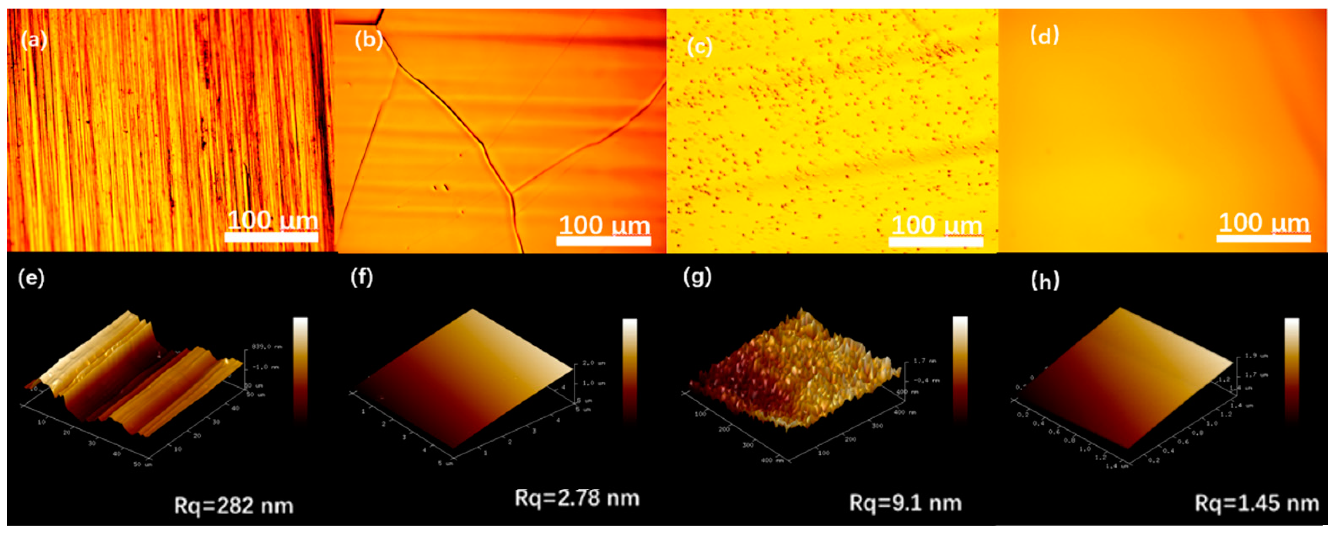
The surface roughness of the substrates obtained by different treatment methods are shown in
Figure 1e–h. The surface roughness of substrates under different treatments is shown in
Table 1.
2.3. Transfer
The hexagonal boron nitride prepared on the copper-nickel substrate needed to be transferred to the SiO2/Si substrate. We used the PMMA-assisted method to transfer it to the SiO2/Si substrate. First, we spin-coated a layer of PMMA on the surface of the copper-nickel substrate grown with hexagonal boron nitride and dried it on a hot stage at 150 °C for 10–30 min. Then, using KOH solution as the solution, copper-nickel substrate as the negative electrode, metal platinum as the positive electrode, and using a 2.7 V DC power supply, the PMMA-coated hexagonal boron nitride was peeled off by generating hydrogen bubbling at the negative electrode and then transferred. In deionized water, it was repeatedly washed several times, and then we used the SiO2/Si substrate to pick up the film. After removing moisture in an oven, we removed PMMA with acetone solution. At this point, our thin film of hexagonal boron nitride was transferred to the target substrate.
2.4. Characterization
The microscopic morphology of the samples was characterized by an optical microscope (Olympus BX53M, Tokyo, Japan) and a scanning electron microscope (SEM, Hitachi S-4800, Tokyo, Japan), and the distribution of elements in the prepared copper-nickel alloy substrate was analyzed by an energy dispersive spectrometer equipped (EDS, Oxford Instruments, Bognor Regis, UK) with SEM. Since h-BN does not have any contrast on the surface of the metal substrate, it is not easy to observe directly by an optical microscope (OM). Here, we applied the characterization of the antioxidant properties of h-BN. The metal substrate after the growth of h-BN was oxidized in the air. Since the area covered by h-BN is not easily oxidized, the area not covered by h-BN is directly oxidized, which could well display the microstructure of h-BN. To enhance the optical contrast of metal substrate samples under an optical microscope, they are generally oxidized in air at 200 °C for 5 min before observation. The surface chemical properties of the samples were analyzed by X-ray photoelectron spectroscopy (XPS, ESCALAB 250 Thermo Fisher SCIENTIFIC, Waltham, MA, USA), and the test results were calibrated with C 1s (284.8 eV). In addition, the h-BN film was analyzed by a Raman spectrometer (Raman, LabRAM HR 800, Jobin Yvon, France), and the wavelength used for the test was 532 nm.
3. Results and Discussion
For Cu-Ni alloys, due to the similar atomic structures of the two, the difference in the atomic radii is small. Nickel atoms can penetrate the lattice of copper atoms to occupy the junction positions of copper atoms. The solute atom Ni can replace part of the lattice of the solvent atom Cu, and the crystal structure of the new substance remains the same as that of the solvent atom, forming a Cu-Ni solid solution. The higher temperature ensures that the diffusion is fully carried out and the internal element distribution is uniform. The Cu foils were first cleaned, polished, annealed, nickel-plated, and re-annealed, which could increase the surface flatness and the average size of the grains.
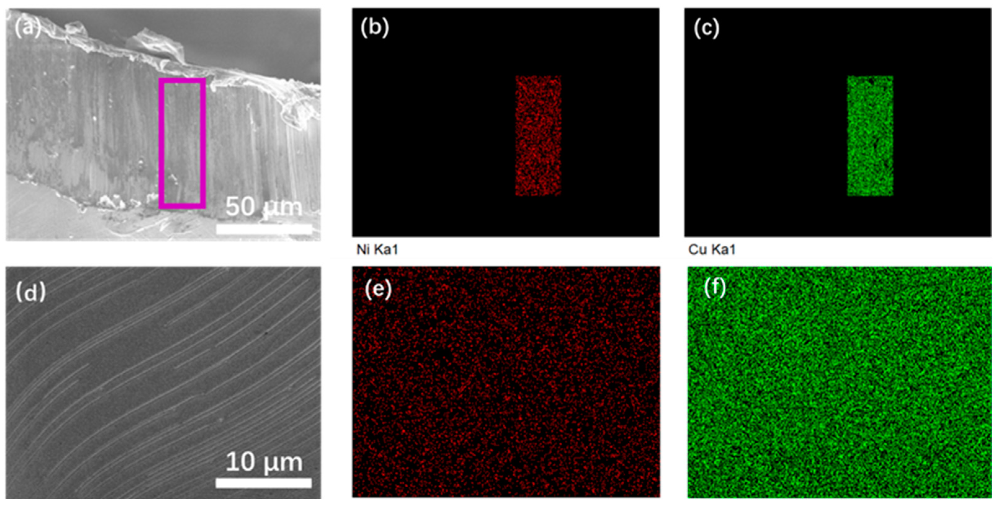
Figure 2 shows the SEM images of the surface morphology and cross-sectional morphology of the Cu-Ni alloy after plating for 30 min and high-temperature treatment, as well as the energy spectrum scanning images of the corresponding area. From the cross-sectional view, the nickel layer plated on the surface of the copper foil was uniformly diffused into the copper foil to form a uniform Cu-Ni alloy (
Figure 2a–c). One could see from
Figure 2d that the surface of the Cu-Ni alloy was very uniform and there was no obvious crystal nucleus precipitation. Ni atoms diffused uniformly on the surface of the Cu foil and penetrated the interior, indicating the formation of a uniform Cu-Ni alloy (
Figure 2e,f). There is no doubt that further prolonging the electroplating time could increase the quality of the Ni layer deposited on the surface of the copper foil and the content of Ni in the alloy. In addition, combined with an energy dispersive X-ray spectroscopy (EDS), the composition ratio of copper and nickel atoms in the Cu-Ni alloy was obtained (
Table 2). We analyzed the quality of the metal foil before and after the electroplating experiment and before and after the annealing treatment by analytical balance. The quality change was calculated and the content of Ni in the Cu-Ni alloy was calculated to be 5%, which was consistent with the alloy ratio measured by EDS.
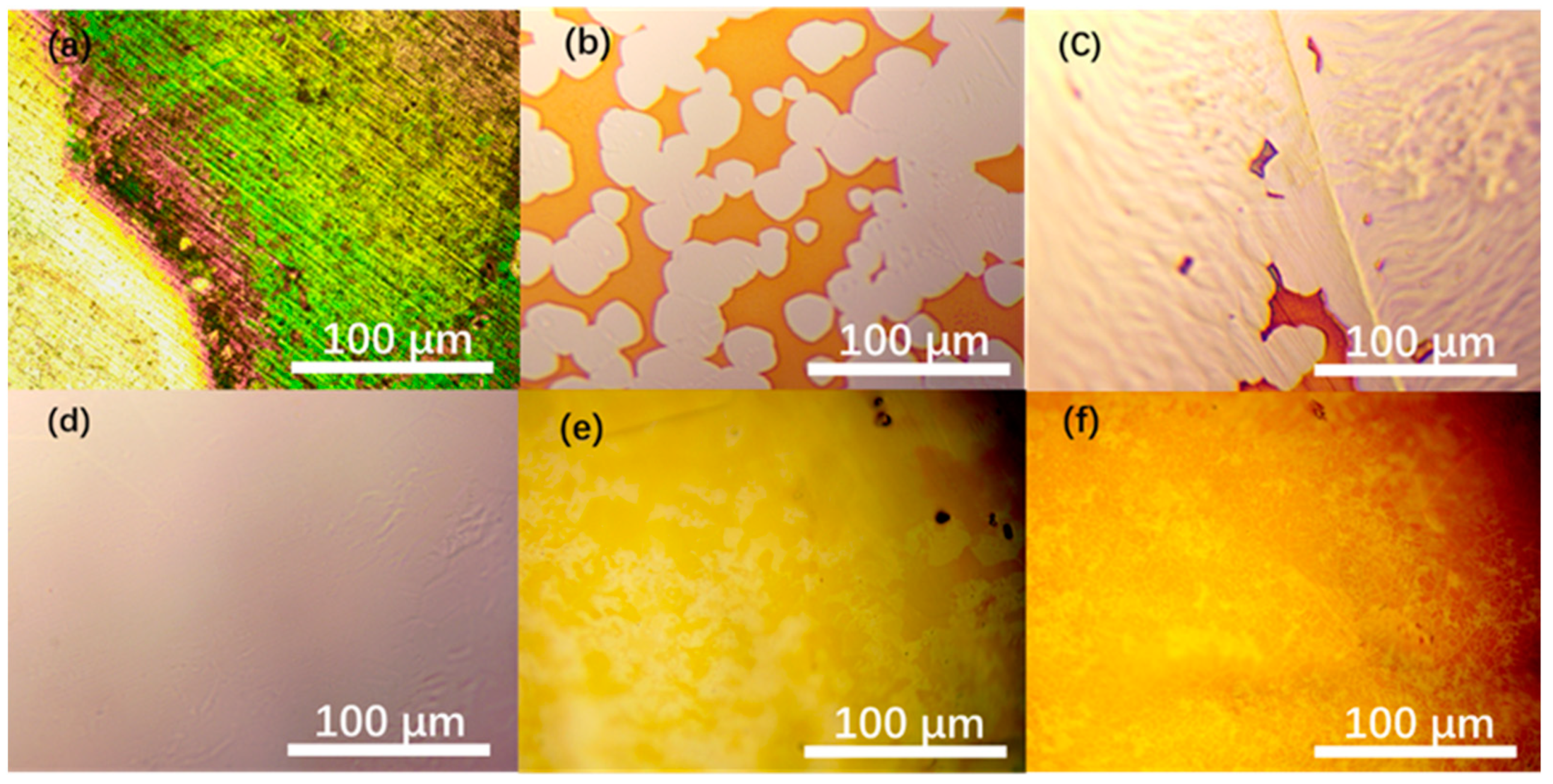
The growth trend and morphology change of h-BN by heating and oxidizing the grown substrate in the air with the prolongation of the reaction time are shown in
Figure 3 and
Figure 4. Within 1 min of the reaction, h-BN did not start growing on the substrate (
Figure 3a). Over time, h-BN gradually started to deposit on the substrate. When the reaction was performed for 5 min, the hexagon grown h-BN on the substrate could be clearly seen (
Figure 3b). After 10 min of reaction, the h-BN on the substrate was connected to form a film, which completely covered the surface of the substrate to form a few-layer structure. In the subsequent process, with the continuous deposition of h-BN, the number and thickness of h-BN layers continued to increase. The multi-layer film structure could be clearly seen when the reaction time reached 11 min, and the multi-layer structure became more obvious with the prolongation of the reaction time. It is worth noting that the size of the as-obtained h-BN film was in the order of hundreds of microns, and the area was much larger than that of the h-BN film prepared by the APCVD method reported previously [
16]. In order to further study the structural characteristics of the h-BN film and its application performance as an ultraviolet optoelectronic device, the samples obtained by the reaction for 10 min were selected to carry out follow-up research work.
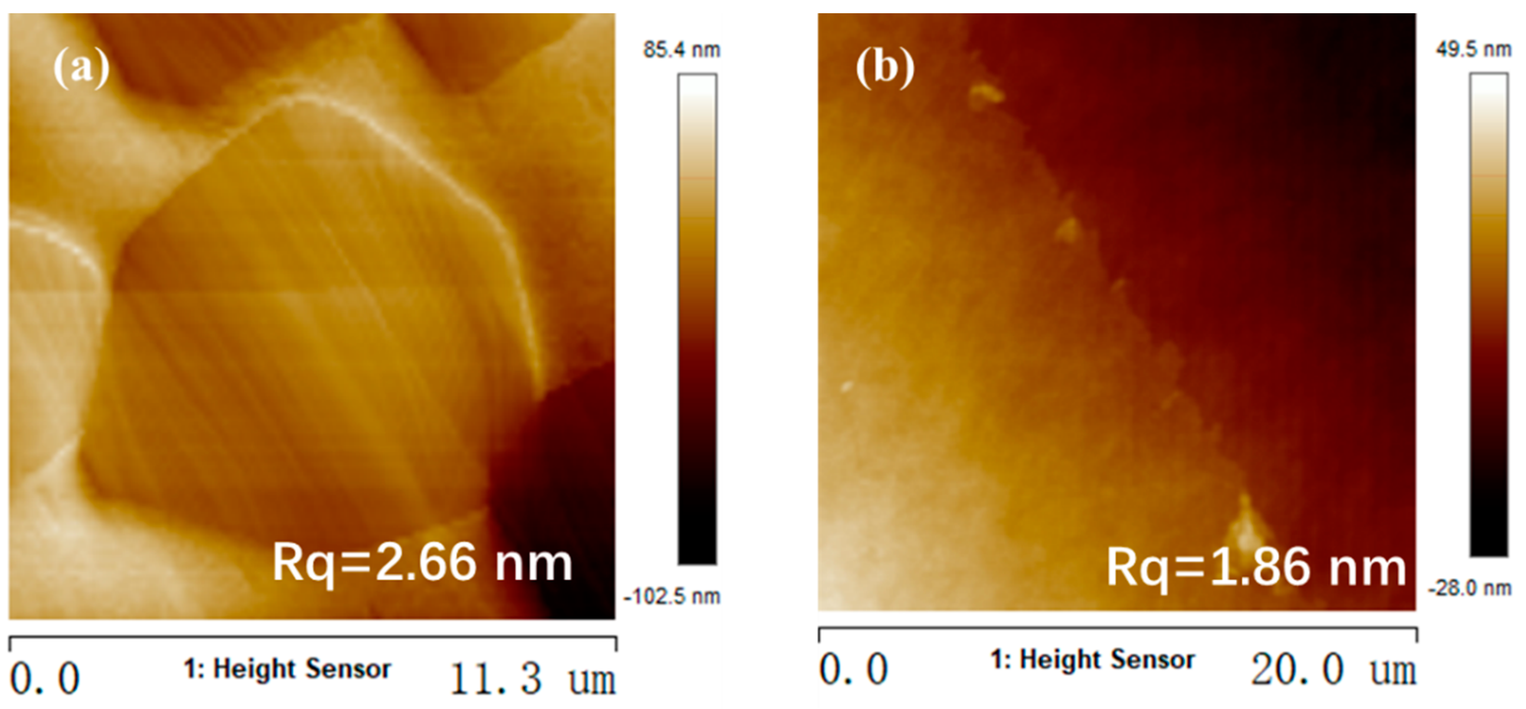
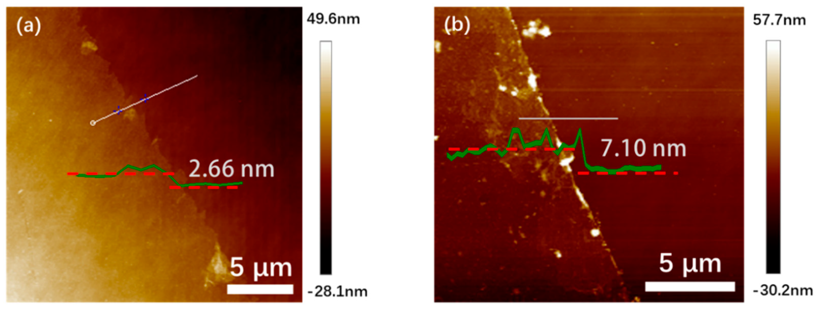
The roughness of an h-BN single crystal was Rq = 2.66 nm, and the roughness of an h-BN thin film was Rq = 1.86 nm (
Figure 5). The thickness of the h-BN film prepared after 11 min of growth was 2.66 nm by atomic force microscopy observation of the step between the film and the substrate, and the thickness of the h-BN film prepared after 15 min of growth was 7.10 nm, as shown in
Figure 6.
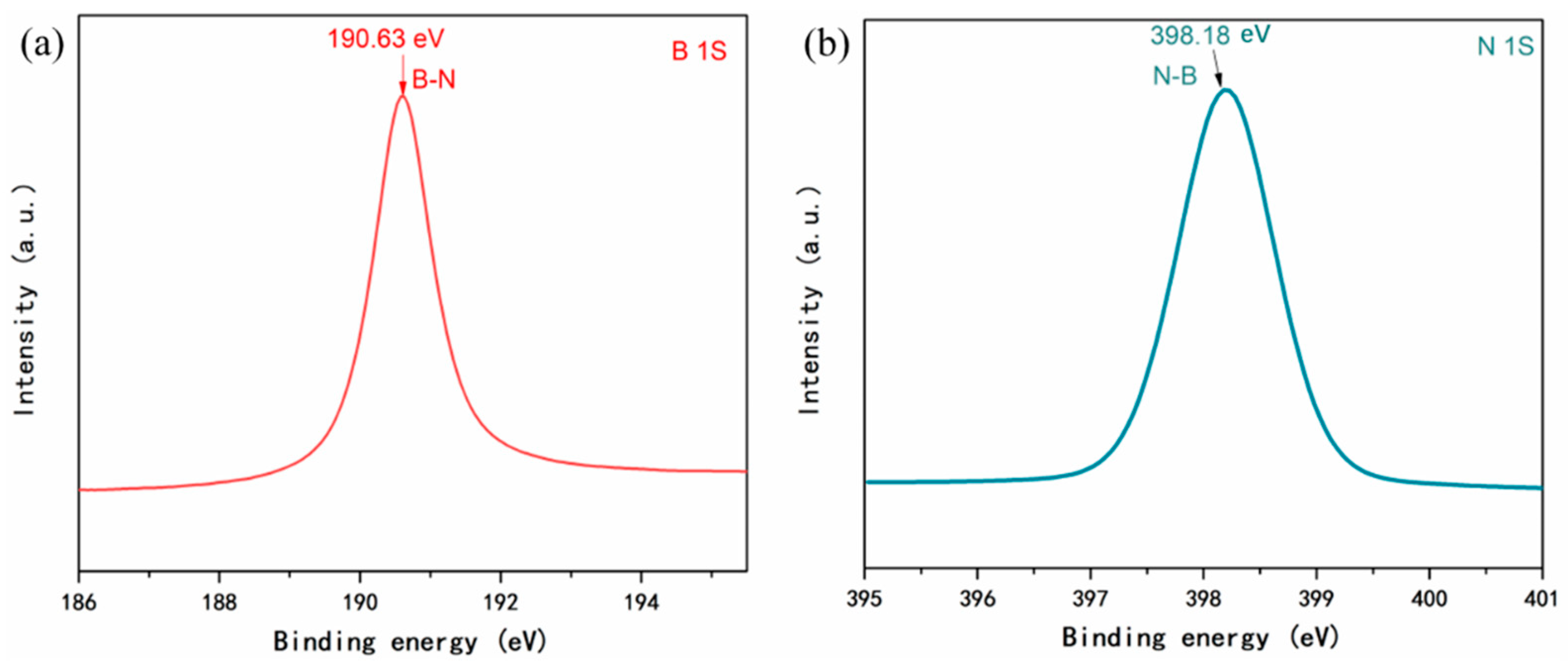
The surface chemical properties of the samples were analyzed by XPS, and the results were corrected with C 1s (284.8 eV). The XPS peaks at 190.63 eV and 398.18 eV were attributed to B 1s and N 1s in the B-N bond (
Figure 7), respectively, which are consistent with the XPS of h-BN reported in the literature [
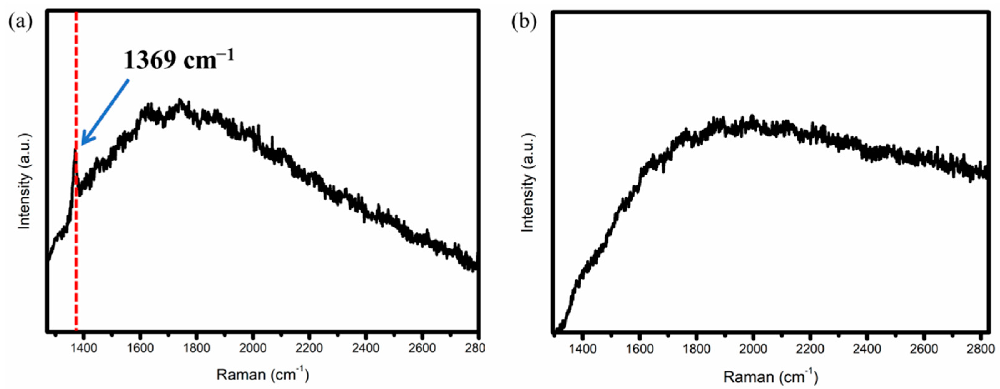
7], indicating that h-BN films were successfully obtained. In addition, the as-obtained h-BN film was further analyzed using Raman spectroscopy (
Figure 8). In order to avoid the influence of the substrate on the test results, we chose to transfer the h-BN film from the Cu-Ni alloy substrate to the SiO
2/Si surface for testing and use SiO
2/Si as the control. Compared with SiO
2/Si (
Figure 5b),
Figure 5a shows an obvious characteristic Raman peak of h-BN E
2g at 1369 cm
−1. It was further proved that we obtained an h-BN film by the APCVD mothed.
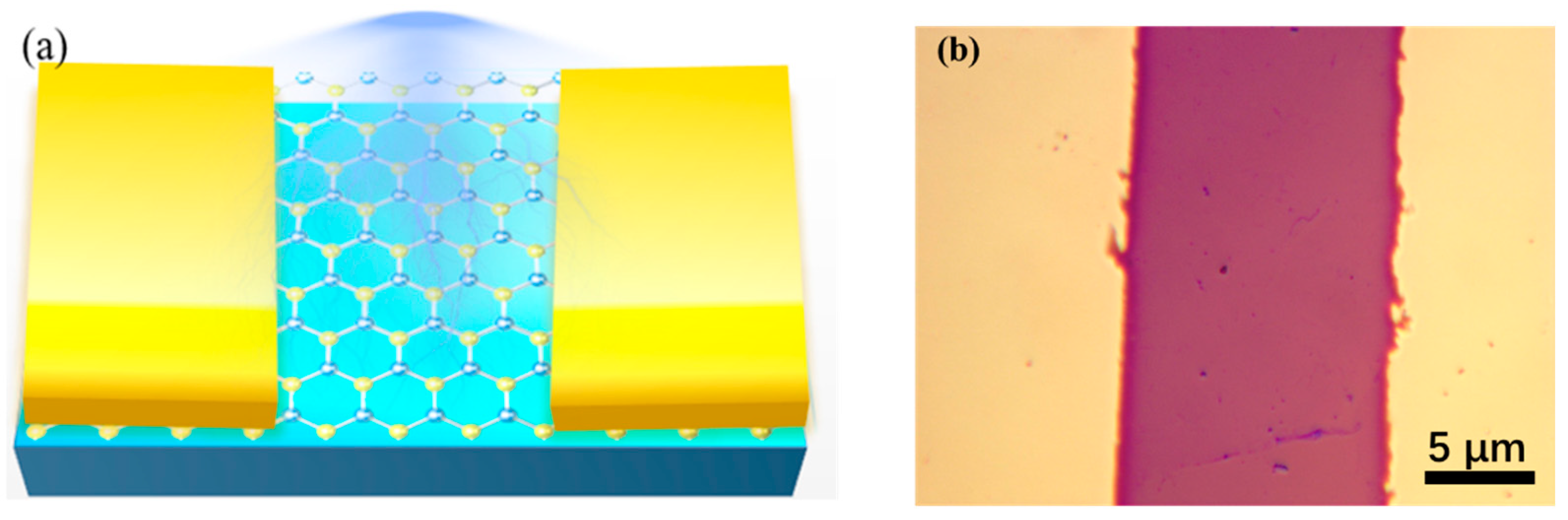
In order to study the application performance of h-BN as a UV photodetector, we used the obtained h-BN film as the channel material and fabricated UV detection photoelectric devices via the mask method and metal deposition method.
Figure 9 shows the schematic and optical microscope images of the device. When fabricating the device, firstly, the h-BN film grown on the Cu-Ni alloy containing 5% Ni was transferred to the SiO
2/Si surface under the optical microscope to construct the device. Then, the h-BN film was masked and only the two ends were left outside. Finally, 25 nm Au electrodes were deposited on the exposed areas at both ends using a thermal evaporation coater to form metal electrodes to obtain ultraviolet optoelectronic devices.
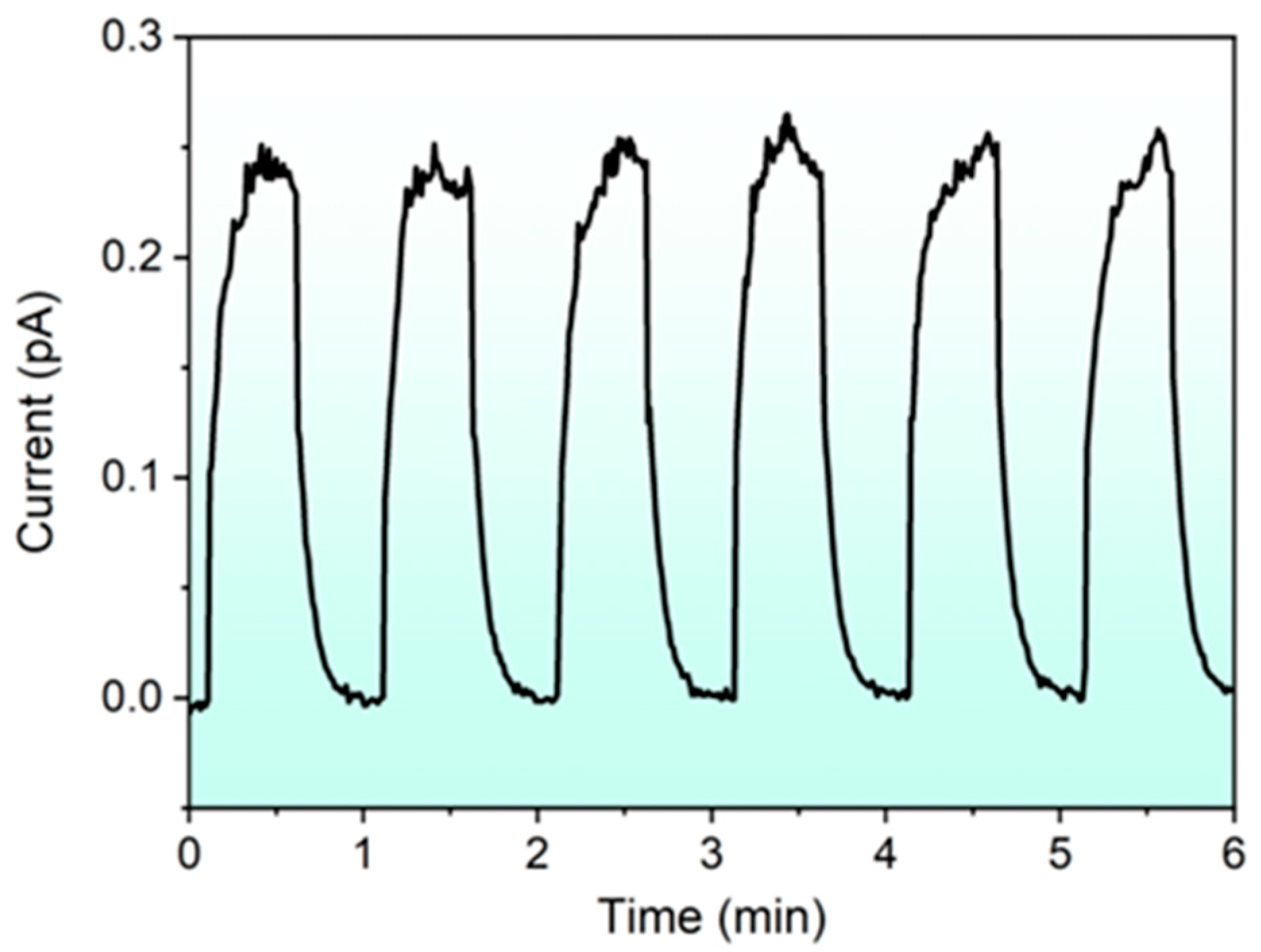
The photoelectric response performance of the device was tested by a temperature-variable probe analysis station (Lakeshore) and semiconductor tester (4200-SCS). We used a DD2.5TZ deuterium lamp as the UV light source, the power of which was 30 W. The photoresponse characteristic and stability of UV detectors were studied by cycling on-off the UV light source (
Figure 10). When the UV light source was turned on, the number of charge carriers increased immediately, resulting in a dramatic increase in the photocurrent observed at the left edge of each current pulse. When the light source was turned off, the photocurrent dropped to the starting position. Repeatedly turning on-off the UV light source showed little deviation in the photocurrent intensity and duration period, indicating that the photoresponse of our device was reversible and stable.


