Abstract
In-grown vacancy defects in bulk and quasi-bulk GaN crystals have been extensively studied with positron annihilation spectroscopy. High concentrations of Ga-vacancy-related defects are found irrespective of the growth method used in crystals with a high O contamination or intentional O doping, and they act as the dominant compensating native defect for n-type conductivity. Low-temperature crystal growth also leads to high concentrations of Ga-vacancy-related defects. Ga vacancies are present in the crystals as a part of the different types of complexes with O, H, and/or VN, depending on the growth conditions.
1. Introduction
The electronic properties of a semiconductor depend on its defects and impurities, and hence can be tuned by doping and achieving low defect densities in true bulk crystals. In GaN, Si is the dopant of choice for achieving n-type conductivity, and p-type conductivity in GaN is obtained by doping with Mg [1]. The use of other dopants, such as Ge for n-type conductivity [2,3] and, e.g., Fe, C, or Mn for semi-insulating or highly resistive material [4,5], have also been previously explored. The knowledge on how these dopants behave and are introduced into the GaN lattice is mostly based on epitaxial growth, where the growth chemistry and purity of the environment are highly controlled owing to the low operational pressure. The growth conditions also control the formation of point defects that typically act as compensating centers for the electrical activity targeted by doping.
The introduction of dopant impurities and the formation of point defects in bulk crystal growth of GaN has been much less studied. High nitrogen pressure solution (HNPS) growth [6], which is the closest to thermodynamic equilibrium, leads to point defect distributions that can be directly compared with theoretical predictions that assume equilibrium [7]. In comparison, the widely used halide vapor phase epitaxy (HVPE) [8,9] and ammonothermal (AM) [10] synthesis methods proceed in conditions that are far from equilibrium. In addition, their growth chemistry and kinetic processes are complex. The introduction of impurities and formation of point defects highly depend on the details of the growth process. In this short review, the focus was vacancy defect formation in bulk GaN crystals, which was analyzed using positron annihilation spectroscopy [11]. In addition to the materials grown by HNPS, HVPE, and basic AM, results obtained in the crystal growth by the Na-flux method (NF) [12], acidic AM [13], oxide vapor phase epitaxy (OVPE) [14], and halide-free vapor phase epitaxy (HFVPE) [15] are discussed.
2. Experiment Details
The methods for growing bulk GaN crystals can be roughly divided into two groups: quasi-bulk and true-bulk. The HVPE, OVPE, and HFVPE methods belong to the first group and fundamentally are epitaxial in nature. They are characterized by a relatively high temperature (1000–1250 °C) and low pressure (~100 kPa) during growth, allowing for high growth rates of the order of 100 μm/h. The threading dislocation (TD) densities are above 106 cm−2, and the concentrations of unintentional impurities (mainly oxygen) are typically below 1017 cm−3. The true-bulk growth methods, namely acidic and basic AM, HNPS, and NF, exhibit a much wider variation in growth temperature (500–1500 °C) and pressure (ranging from megapascals to gigapascals), but are all considered to be high-pressure and share low growth rates (typically well below 10 μm/h, even less than 0.1 μm/h). The TD densities are low, well below 104 cm−2, while unintentional impurity (mainly oxygen) concentrations are relatively high, above 1018 cm−3. For more details on the materials and the synthesis methods, see Refs. [6,8,9,10,12,13,14,15].
Positron annihilation spectroscopy is a set of methods with particular applications in the identification and quantification of negatively charged, neutral-vacancy-type defects in semiconductors [11], and has been widely applied in studying III-nitrides [16,17,18,19,20,21,22,23,24,25]. The Ga vacancy (VGa) appears in complexes with a donor-type defect on the N sublattice, such as residual substitutional oxygen (ON) [26] or a N vacancy (VN) [22]. Additionally, Ga-vacancy–hydrogen complexes are important [27]. In general, the cation vacancies and their complexes are deep acceptors, thus compensating for their n-type conductivity and adding to the scattering centers, limiting the carrier mobility in these materials. N vacancies not associated with Ga vacancies can trap positrons in systems with reduced dimensionality [28,29], but not in bulk crystals.
Positrons implanted into a sample can become trapped, localizing at neutral and negative vacancies due to the missing positive ion core. The trapping of positrons at these defects is observed as a well-defined change in the positron-electron annihilation radiation, i.e., as an increase in the positron lifetime and a narrowing of the momentum distribution of the annihilating positron–electron pair (Doppler broadening). The combination of experimental techniques with theoretical calculations provides the means to deduce both the identities (sublattice, decoration by impurities) and the concentrations of the vacancies [11]. The concentration sensitivity range is 1015–1019 cm−3. Performing measurements as a function of temperature gives information on the charge states of the detected defects.
Bulk GaN crystals have been studied by using all of the above-mentioned approaches, using both fast positrons, where a positron source (22Na) is sandwiched between two identical pieces of sample material, and slow positron beams, where positrons from a radioactive source are slowed down and implanted in a single sample at energies between 0–40 keV. Fast positrons probe the sample up to about 200 μm, providing averaged data over these depths. Slow positron beams are used to probe near-surface regions up to 2 μm below the surface. Typical bulk GaN crystal samples studied using positrons have lateral dimensions in the 5–10 mm range, and a thickness of about 0.5 mm. Most of the positron lifetime results discussed in this study were obtained with fast positron experiments, while most of the Doppler broadening data were obtained by employing slow positron beams. The positron lifetime spectra were analyzed as the sum of exponential decay components, convoluted with the Gaussian timing resolution function of the spectrometer. The increase in the average lifetime τave above the bulk lattice lifetime τB indicates the presence of vacancy defects in the material. In the case of one type of vacancy defect with specific lifetime τV, the decomposition of the lifetime spectrum into two exponential decay components is straightforward to interpret. The second lifetime component τ2 = τV directly gives the vacancy-specific lifetime, and the first lifetime component is τ1 = (τB−1 + κV)−1 < τB, where τB is the positron lifetime in the delocalized state in the lattice, and κV is the positron trapping rate in the vacancy defects. In the case of GaN crystals, τB ≈ 160 ps and τV = 235 ± 10 ps for Ga vacancies and Ga vacancy–oxygen complexes, respectively [16,26,30].
The Doppler broadening of the 511 keV annihilation peak is often characterized by the S and W parameters. These are defined as the normalized areas (counts) of the center and wings of the peak, respectively. They are a measure of the fraction of positrons annihilating with low-momentum electrons (S) and high-momentum electrons (W). The S (W) parameter is a linear superposition of the characteristic S (W) parameters for annihilations in different positron states in the sample. The presence of vacancies results in a higher S parameter and, correspondingly, a lower W parameter than in a defect-free lattice. If only one type of vacancy traps positrons, (S,W) becomes a linear combination of the values (SB,WB) and (SV,WV), corresponding to the lattice and the vacancy, respectively. The measured values would thereby fall on a straight line connecting the points (SB,WB) and (SV,WV) on an S–W plot. The position on this line reveals the concentration of these vacancies.
3. Overview of Positron Results in GaN Crystals
3.1. True-Bulk GaN Crystals
The positron annihilation experiments performed in the mid-1990s on HNPS-grown GaN crystals demonstrated that Ga vacancies are the dominant native acceptor defects in n-type GaN [16]. The growth environment is characterized by a high temperature (~1500 °C) and very high pressure (~1 GPa). This environment leads to a relatively high O contamination in the crystals (at the level of [O] ~1019–1020 cm−3) and naturally high n-type conductivity. For details on the crystal growth, see Ref. [6] and the references therein.
Figure 1 shows the average positron lifetime, measured as a function of temperature in both unintentionally doped as well as Mg- and Be-doped HNPS GaN crystals. The average positron lifetimes are displayed together with the second lifetime component extracted from the lifetime spectra [16,31,32]. The latter exhibits a value of τ2 = 235 ± 10 ps that is identified as originating from Ga-vacancy-related defects. The temperature behavior of the average lifetime in the undoped HNPS GaN crystal is indicative of the competition between negative-ion-type defects that act as shallow positron traps and negatively charged Ga vacancies. Detailed analysis shows that the negative ions that dominate at low temperatures are associated with residual Mg in the material, while the concentration of negatively charged Ga vacancies is of the order of 1017 cm−3. With the intentional addition of Mg dopants, the average lifetime and Ga vacancy concentration decreases. In the highly Mg-doped HNPS GaN crystal, no evidence of Ga vacancies is observed. This is in line with thermal vacancy formation being the dominant mechanism [33,34], as the Fermi level shifts toward the middle of the gap with increased Mg doping. Be doping also reduces the Ga vacancy concentration, but not as efficiently as Mg due to Be’s ability to easily switch between interstitial and substitutional positions at the high growth temperatures [32].
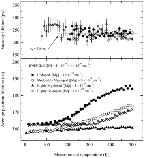
Figure 1.
The average positron lifetime, measured as a function of temperature in HNPS bulk GaN crystals with different impurity and dopant concentrations. The second lifetime component separated from the lifetime spectra is shown in the upper panel, where the line shows the value specific to the Ga vacancy. Data adapted from Refs. [16,31,32].
AM growth of GaN crystals has seen tremendous development in the past 20 years [10,13,35,36,37]. The growth environment is characterized by low temperature (~500 °C) and high pressure (~1 MPa). There are two main variants of the technique, depending on whether acidic or basic mineralizers are employed, with the latter being the more popular choice. As in HNPS growth, O contamination is relatively high, but careful tuning of the growth processes can push the O concentrations down to ~1018 cm−3. For details on the crystal growth, see Refs. [13,36,37] and the references therein.
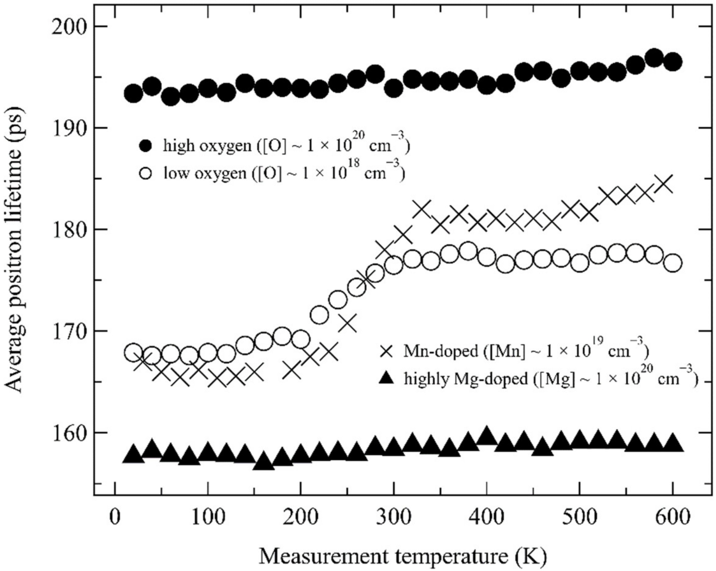
Figure 2 shows the average positron lifetime, measured as a function of temperature in both unintentionally doped as well as Mg- and Mn-doped GaN crystals, grown by basic AM [37,38,39]. The temperature behavior of the average positron lifetime appears to be similar to that of the HNPS crystals. In particular, the highly Mg-doped basic AM crystal shows identical behavior to the Mg-doped HNPS crystal, indicative of no vacancy defects. However, despite the average positron lifetime being higher than the bulk lattice lifetime of ~160 ps in GaN in the other samples, no second lifetime component can be extracted in the positron lifetime spectra. Detailed analysis of lifetime data in the wide selection of basic GaN AM crystals with varying O, Mg, and Mn concentrations [38,39,40] has led to the interpretation that the Ga vacancies are complexed with multiple hydrogen atoms in these samples. These exhibit clearly shorter vacancy-related lifetimes. Hence, the similarity to the HNPS crystals is only apparent, and the Ga vacancy concentrations in the basic AM crystals are one or two orders of magnitude higher, in the 1019 cm−3 range. This indicates that despite the strong dependence of the average positron lifetime on the O content, the thermal formation of vacancies is not the dominant mechanism in AM growth, as the Ga vacancy concentrations should then be lower than in HNPS GaN growth. There are less studies of acidic AM GaN crystals [41], but the results are in line with the findings in basic AM GaN: high concentrations of Ga vacancies complexed with multiple hydrogen atoms.

Figure 2.
The average positron lifetime, measured as a function of temperature in AM bulk GaN crystals with different impurity and dopant concentrations. All the positron lifetime spectra contained only one decay component. Data adapted from Refs. [38,39,40].
The NF synthesis method is an emerging approach for growing high-quality bulk GaN crystals [12]. The growth temperature is between those of HNPS and AM (~900 °C) and the high-pressure conditions are similar to AM (a few megapascals). The O contamination is relatively high (1018–1019 cm−3) and is nonuniform due to the strong faceting during growth and the differences in O incorporation on different growth surfaces [6,33,42,43]. Details on the growth method can be found in Refs. [44,45].
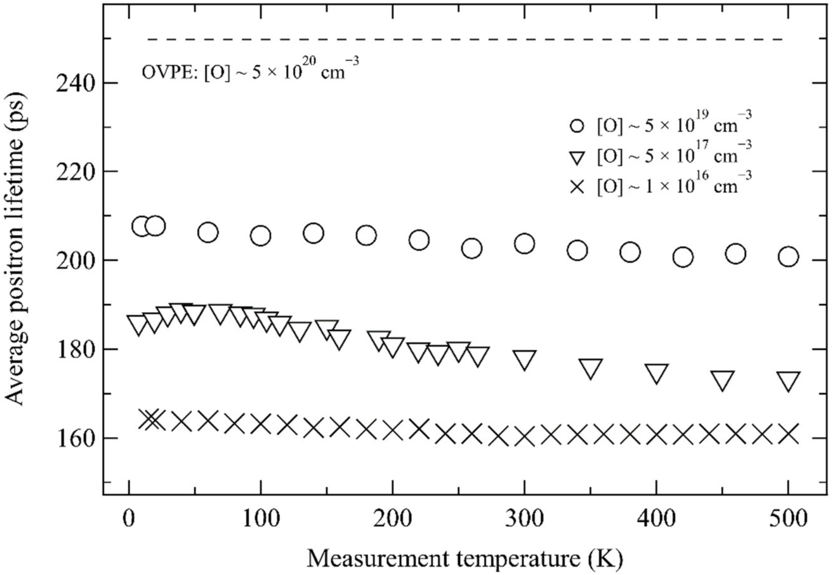
A combined positron lifetime and Doppler broadening study [42] on the different growth regions in NF GaN crystals shows that the vacancy formation in this material is also strongly dependent on the O incorporation. The positron lifetime experiments performed at room temperature reveal a second lifetime component τ2 = 240–250 ps, somewhat longer than that found in HNPS GaN crystals. The concentration of these Ga-vacancy-related defects increases with O concentration, and they are interpreted to account for the loss in transparency of the crystals. The Doppler broadening results lead to the interpretation that the Ga vacancies found in the NF GaN crystals are coupled with one or more N vacancies, forming small vacancy clusters. Additionally, the NF GaN crystals with the lowest O content and highest transparency show no evidence of Ga vacancies.
3.2. Quasi-Bulk GaN Crystals
Halide vapor phase epitaxy (HVPE) is the present-day method of choice for the large-scale manufacture of GaN substrates. As the name suggests, it is fundamentally an epitaxial synthesis method from the vapor phase, characterized by low operating pressure compared to the true-bulk synthesis techniques (~100 kPa). The growth temperatures are in the range of 1000–1250 °C, with only the HNPS method exhibiting higher temperatures. Oxygen contamination and other types of impurities are very low due to the lower growth pressure, in the amount of [O] ~1016 cm−3 or less. Variants of the HVPE technique have also started to emerge, with the purpose of tackling some of the long-term stability issues related to the formation of NH4 Cl and its accumulation in the reaction chambers. Halide-free vapor phase epitaxy (HFVPE) employs the approach of directly reacting gaseous Ga with ammonia (instead of intermediate GaCl), while oxide vapor phase epitaxy (OVPE) employs gallium oxide reacting with ammonia. For further details on these methods, see Refs. [8,9,14,15,46] and the references therein.
Figure 3 shows the average positron lifetime, measured as a function of temperature in HVPE GaN crystals with different O concentrations [26,30,47,48]. OVPE samples were studied only at room temperature [48], exhibiting a very similar average lifetime and shown as the dashed line in the figure. The temperature behavior differs from what is displayed in Figure 1 and Figure 2 as the residual concentrations of acceptor-type (negatively charged) impurities are significantly lower in HVPE GaN growth. The data in Figure 3 indicate the presence of only Ga-vacancy-related defects in the negative charge state and no other negative defects. The Ga vacancy concentrations range from ~1 × 1015 cm−3 (close to the detection limit) to more than 1019 cm−3, depending on the O concentration. As similarly observed in HNPS growth, thermodynamic considerations favor the interpretation that thermal vacancy formation is the dominant mechanism in HVPE growth [34]. In the referenced paper, the Ga vacancy formation energy was determined as Ef = 2.5–3.2 eV at a Fermi level position of EC − EF = 0.5 eV, which was accomplished by combining the positron lifetime and Doppler broadening experiments. It should be noted that most of an HVPE GaN sample is low-impurity material, meaning that HVPE GaN is often used as the “defect-free” reference sample for positron studies in GaN, as the low concentration of Ga vacancies is only detected below room temperature [21,22,30]. HFVPE GaN samples also exhibit low impurity levels, and no evidence of Ga vacancy defects was found [49], even if the Si content is somewhat higher than in the purest HVPE GaN samples.
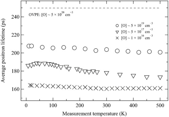
Figure 3.
The average positron lifetime, measured as a function of temperature in HVPE GaN crystals with different oxygen concentrations. The second lifetime component (not shown) separated from the lifetime spectra coincides with the Ga vacancy value found in HNPS GaN. The dashed line shows the room temperature value obtained in OVPE GaN. Data adapted from Refs. [26,30,47,48].
4. Discussion
The true-bulk and quasi-bulk GaN crystals exhibit one feature in common when studied with positrons: if oxygen is the dominant impurity, the formation of Ga-vacancy-related defects during growth is dictated by the O concentration. The greater the oxygen concentration, the greater the concentration of Ga vacancies. The examples of HVPE, HFVPE, and NF growth show that it is possible to synthesize bulk GaN crystals by different methods in a way that leads to varying Ga vacancy concentrations, even below the detection limit of about 1016 cm−3 at room temperature if the O content is low enough. The dependence on oxygen is interesting, as it does not appear to be a function of the vacancy formation mechanism. In AM growth, where the temperature is significantly lower than in the other methods, vacancy concentrations are the highest. Therefore, it would seem that not only does O affect the vacancy formation through the Fermi level position and VGa-ON binding energy [34], but also modifies the kinetics at the growth surface by its presence.
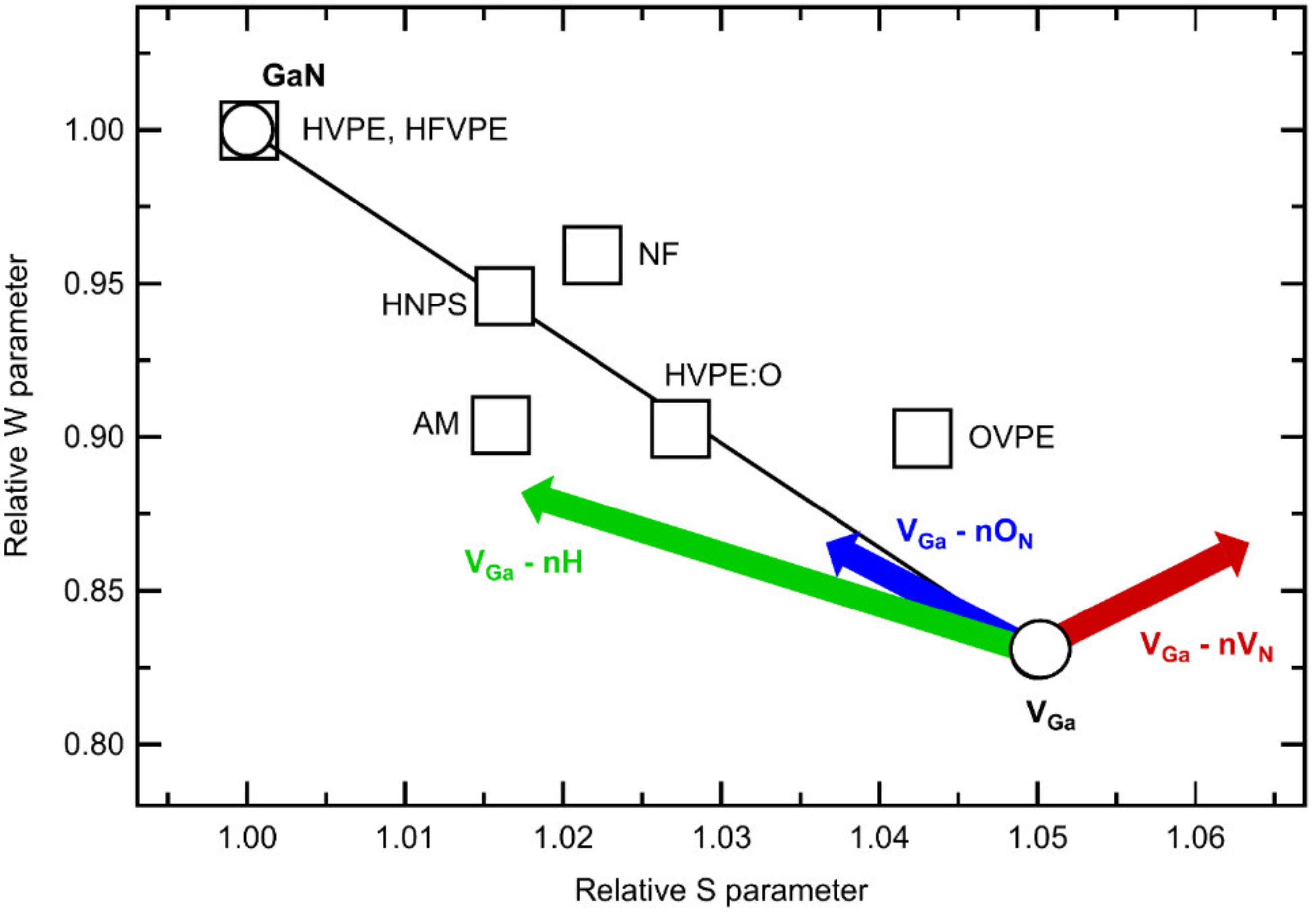
The nature of the Ga-vacancy-related defects is not the same as those found in GaN crystals grown by different methods. Figure 4 collects the Doppler broadening data obtained in the different types of GaN crystals studied with positrons, combined with the results of theoretical calculations for various positron states [11,32,41,42,48,49,50,51]. If all of the studied crystals only contained differing concentrations of pure isolated VGa, all of the experimental data (squares) would fall on the line that connects GaN and VGa. A detailed comparison of theoretical calculations with experiments allows for the identification of the features related to complex formation between VGa, H, O, and VN, shown by the colored arrows in the (S, W) plot [32,50,51]. Low-oxygen HVPE and HFVPE produce data that are similar to those of the GaN lattice, while HNPS and HVPE with excess oxygen are likely to contain VGa–ON (or isolated VGa, but this is less likely, as discussed in Refs. [33,34]). The high Ga vacancy concentrations in basic and acidic AM GaN are identified as VGa–nH complexes. On the other hand, NF with high oxygen content and OVPE are interpreted to contain VGa–nVN complexes.

Figure 4.
The typical relative (S, W) Doppler parameters measured in bulk and quasi-bulk GaN crystals (squares). The parameters of the isolated VGa obtained by combining experiments and state of the art theoretical calculations are shown with the circle, and the arrows depict the calculated effects of complex formation with O, H, and VN. Data adapted from Refs. [11,32,41,42,48,49,50,51].
HNPS, HVPE, and HFVPE GaN crystals are grown at the highest temperatures (above 1000 °C), and the behavior of the Ga vacancies operates as a function of the O content. The identity of the crystals can be fully understood by the thermodynamic considerations and comparing ab initio theoretical calculations [34]. OVPE GaN crystals should belong to this category as well, but the excessively high O concentrations that are close to 1021 cm−3 appear to complicate the interpretations. The presence of ammonia in the growth environment appears to be the key to the extremely high Ga vacancy concentrations and their complexes with multiple H atoms, as observed in AM GaN. NF-grown GaN crystals that also exhibit strong vacancy clustering (VGa–nVN complexes) have much lower vacancy concentrations, possibly owing to the higher growth temperature and improved growth surface kinetics.
Effects of doping on the compensating vacancy defect formation have been studied extensively in thin-film growth of GaN and its alloys [19,20,21,22,23,24,25]. Doping in bulk growth of GaN has been less studied, meaning many aspects concerning dopant activation and compensation by native defects are still unknown. Controlled studies of doping in bulk GaN have the potential to elucidate vacancy formation mechanisms and their dependence on the growth environment. Ion implantation processing combined with high pressure—high-temperature annealing appears to be a promising way to achieve well-defined doping profiles in bulk GaN substrates [52,53].
5. Summary
Positron annihilation spectroscopy has been extensively employed to study vacancy defects in bulk and quasi-bulk GaN crystals over the past 25 years. Ga vacancy defects have been identified as the dominant native acceptor-type defect in n-type crystals, irrespective of the growth method. Even though the formation mechanisms of the Ga vacancy defects strongly depend on the temperature, pressure, and chemistry during synthesis, the amount of O impurities appears as a controlling factor in all GaN crystals: the greater the oxygen concentration, the greater the concentration of Ga vacancies. High-temperature growth favors the formation of VGa–ON complexes, while crystals grown at low temperatures and in the presence of ammonia contain VGa–nH complexes. Other extreme conditions may lead to the formation of VGa–nVN clusters and more complex defect configurations.
Funding
This work was partially supported by the Academy of Finland Grant 315082.
Data Availability Statement
No new data were created or analyzed in this study. Data sharing is not applicable to this article.
Conflicts of Interest
The author declares no conflict of interest.
References
- Morkoç, H. Handbook of Nitride Semiconductors and Devices; Wiley-VCH: Weinheim, Germany, 2008. [Google Scholar]
- Iwinska, M.; Takekawa, N.; Ivanov, V.Y.U.; Amilusik, M.; Kruszewski, P.; Piotrzkowski, R.; Litwin-Staszewska, E.; Lucznik, B.; Fijalkowski, M.; Sochacki, T.; et al. Crystal growth of HVPE-GaN doped with germanium. J. Cryst. Growth 2017, 480, 102. [Google Scholar] [CrossRef]
- Fireman, M.N.; L’Heureux, G.; Wu, F.; Mates, T.; Young, E.C.; Speck, J.S. High germanium doping of GaN films by ammonia molecular beam epitaxy. J. Cryst. Growth 2018, 508, 19–23. [Google Scholar] [CrossRef]
- Heikman, S.; Keller, S.; Denbaars, S.; Mishra, U.K. Growth of Fe doped semi-insulating GaN by metalorganic chemical vapor deposition. Appl. Phys. Lett. 2002, 81, 439–441. [Google Scholar] [CrossRef]
- Amilusik, M.; Zajac, M.; Sochacki, T.; Lucznik, B.; Fijalkowski, M.; Iwinska, M.; Wlodarczyk, D.; Somakumar, A.K.; Suchocki, A.; Bockowski, M. Carbon and Manganese in Semi-Insulating Bulk GaN Crystals. Materials 2022, 15, 2379. [Google Scholar] [CrossRef]
- Grzegory, I.; Leszczynski, M.; Krukowski, S.; Perlin, P.; Suski, T.; Porowski, S. The Application of High Pressure in Physics and Technology of III-V Nitrides. Acta Phys. Pol. A 2001, 100 (Suppl. 57), 57–109. [Google Scholar] [CrossRef]
- Lyons, J.L.; Van de Walle, C.G. Computationally predicted energies and properties of defects in GaN. NPJ Comput. Mater. 2017, 3, 12. [Google Scholar] [CrossRef]
- Geng, H.; Sunakawa, H.; Sumi, N.; Yamamoto, K.; Yamaguchi, A.A.; Usui, A. Growth and strain characterization of high quality GaN crystal by HVPE. J. Cryst. Growth 2012, 350, 44–49. [Google Scholar] [CrossRef]
- Bockowski, M.; Iwinska, M.; Amilusik, M.; Fijalkowski, M.; Łucznik, B.; Sochacki, T. Challenges and future perspectives in HVPE-GaN growth on ammonothermal GaN seeds. Semicond. Sci. Technol. 2016, 31, 093002. [Google Scholar] [CrossRef]
- Dwilińskia, R.; Doradzińskia, R.; Garczyńskia, J.; Sierzputowskia, L.P.; Puchalskia, A.; Kanbarab, Y.; Yagib, K.; Minakuchib, H.; Hayashib, H. Bulk ammonothermal GaN. J. Cryst. Growth 2009, 311, 3015. [Google Scholar] [CrossRef]
- Tuomisto, F.; Makkonen, I. Defect identification in semiconductors with positron annihilation: Experiment and theory. Rev. Mod. Phys. 2013, 85, 1583–1631. [Google Scholar] [CrossRef] [Green Version]
- Mori, Y.; Imade, M.; Murakami, K.; Takazawa, H.; Imabayashi, H.; Todoroki, Y.; Kitamoto, K.; Maruyama, M.; Yoshimura, M.; Kitaoka, Y.; et al. Growth of bulk GaN crystal by Na flux method under various conditions. J. Cryst. Growth 2011, 350, 72–74. [Google Scholar] [CrossRef]
- Mikawa, Y.; Ishinabe, T.; Kawabata, S.; Mochizuki, T.; Kojima, A.; Kagamitani, Y.; Fujisawa, H. Ammonothermal growth of polar and non-polar bulk GaN crystal. Proc. SPIE 2015, 9363, 936302. [Google Scholar]
- Takino, J.; Sumi, T.; Okayama, Y.; Nobuoka, M.; Kitamoto, A.; Imanishi, M.; Yoshimura, M.; Mori, Y. Development of a 2-inch GaN wafer by using the oxide vapor phase epitaxy method. Jpn. J. Appl. Phys. 2019, 58, SC1043. [Google Scholar] [CrossRef]
- Nakamura, D.; Kimura, T.; Horibuchi, K. Halogen-free vapor phase epitaxy for high-rate growth of GaN bulk crystals. Appl. Phys. Express 2017, 10, 45504. [Google Scholar] [CrossRef] [Green Version]
- Saarinen, K.; Laine, T.; Kuisma, S.; Nissilä, J.; Hautojärvi, P.; Dobrzynski, L.; Baranowski, J.M.; Pakula, K.; Stepniewski, R.; Wojdak, M.; et al. Observation of Native Ga Vacancies in GaN by Positron Annihilation. Phys. Rev. Lett. 1997, 79, 3030–3033. [Google Scholar] [CrossRef]
- Rauch, C.; Makkonen, I.; Tuomisto, F. Identifying vacancy complexes in compound semiconductors with positron annihilation spectroscopy: A case study of InN. Phys. Rev. B 2011, 84, 125201. [Google Scholar] [CrossRef] [Green Version]
- Mäki, J.-M.; Makkonen, I.; Tuomisto, F.; Karjalainen, A.; Suihkonen, S.; Räisänen, J.; Chemekova, T.Y.; Makarov, Y.N. Identification of the VAl-ON complex in AlN single crystals. Phys. Rev. 2011, 84, 081204. [Google Scholar] [CrossRef] [Green Version]
- Uedono, A.; Tenjinbayashi, K.; Tsutsui, T.; Shimahara, Y.; Miyake, H.; Hiramatsu, K.; Oshima, N.; Suzuki, R.; Ishibashi, S. Native cation vacancies in Si-doped AlGaN studied by monoenergetic positron beams. J. Appl. Phys. 2012, 111, 013512. [Google Scholar] [CrossRef]
- Uedono, A.; Watanabe, T.; Kimura, S.; Zhang, Y.; Lozac’H, M.; Sang, L.; Ishibashi, S.; Oshima, N.; Suzuki, R.; Sumiya, M. Vacancy-type defects in InxGa1−xN grown on GaN templates probed using monoenergetic positron beams. J. Appl. Phys. 2013, 114, 184504. [Google Scholar] [CrossRef]
- Uedono, A.; Fujishima, T.; Piedra, D.; Yoshihara, N.; Ishibashi, S.; Sumiya, M.; Laboutin, O.; Johnson, W.; Palacios, T. Annealing behaviors of vacancy-type defects near interfaces between metal contacts and GaN probed using a monoenergetic positron beam. Appl. Phys. Lett. 2014, 105, 052108. [Google Scholar] [CrossRef] [Green Version]
- Uedono, A.; Malinverni, M.; Martin, D.; Okumura, H.; Ishibashi, S.; Grandjean, N. Vacancy-type defects in Mg-doped GaN grown by ammonia-based molecular beam epitaxy probed using a monoenergetic positron beam. J. Appl. Phys. 2016, 119, 245702. [Google Scholar] [CrossRef] [Green Version]
- Prozheeva, V.; Makkonen, I.; Cuscó, R.; Artús, L.; Dadgar, A.; Plazaola, F.; Tuomisto, F. Radiation-induced alloy rearrangement in InxGa1−xN. Appl. Phys. Lett. 2017, 110, 132104. [Google Scholar]
- Chichibu, S.F.; Uedono, A.; Kojima, K.; Ikeda, H.; Fujito, K.; Takashima, S.; Edo, M.; Ueno, K.; Ishibashi, S. The origins and properties of intrinsic nonradiative recombination centers in wide bandgap GaN and AlGaN. J. Appl. Phys. 2018, 123, 161413. [Google Scholar] [CrossRef] [Green Version]
- Prozheev, I.; Mehnke, F.; Wernicke, T.; Kneissl, M.; Tuomisto, F. Electrical compensation and cation vacancies in Al rich Si-doped AlGaN. Appl. Phys. Lett. 2020, 117, 142103. [Google Scholar] [CrossRef]
- Hautakangas, S.; Makkonen, I.; Ranki, V.; Puska, M.J.; Saarinen, K.; Xu, X.; Look, D.C. Direct evidence of impurity decoration of Ga vacancies in GaN from positron annihilation spectroscopy. Phys. Rev. B 2006, 73, 193301. [Google Scholar] [CrossRef] [Green Version]
- Suihkonen, S.; Pimputkar, S.; Sintonen, S.; Tuomisto, F. Defects in Single Crystalline Ammonothermal Gallium Nitride. Adv. Electron. Mater. 2017, 3, 1600496. [Google Scholar] [CrossRef] [Green Version]
- Makkonen, I.; Snicker, A.; Puska, M.; Mäki, J.-M.; Tuomisto, F. Positrons as interface-sensitive probes of polar semiconductor heterostructures. Phys. Rev. B 2010, 82, 041307. [Google Scholar] [CrossRef] [Green Version]
- Vera, P.; Ilja, M.; Haoran, L.; Stacia, K.; Umesh, K.M.; Filip, T. Interfacial N Vacancies in GaN/(Al,Ga)N/GaN Heterostructures. Phys. Rev. Appl. 2020, 13, 044034. [Google Scholar]
- Tuomisto, F.; Ranki, V.; Look, D.C.; Farlow, G.C. Introduction and recovery of Ga and N sublattice defects in electron-irradiated GaN. Phys. Rev. B 2007, 76, 165207. [Google Scholar] [CrossRef] [Green Version]
- Saarinen, K.; Grzegory, I.; Lucznik, B.; Nissilä, J.; Hautojärvi, P.; Likonen, J.; Suski, T.; Porowski, S. The influence of Mg doping on the formation of Ga vacancies and negative ions in GaN bulk crystals. Appl. Phys. Lett. 1999, 75, 2441–2443. [Google Scholar] [CrossRef]
- Tuomisto, F.; Prozheeva, V.; Makkonen, I.; Myers, T.H.; Bockowski, M.; Teisseyre, H. Amphoteric Be in GaN: Experimental Evidence for Switching between Substitutional and Interstitial Lattice Sites. Phys. Rev. Lett. 2017, 119, 196404. [Google Scholar] [CrossRef] [PubMed] [Green Version]
- Tuomisto, F.; Saarinen, K.; Łucznik, B.; Grzegory, I.; Teisseyre, H.; Suski, T.; Porowski, S.; Hageman, P.R.; Likonen, J. Effect of growth polarity on vacancy defect and impurity incorporation in dislocation-free GaN. Appl. Phys. Lett. 2005, 86, 031915. [Google Scholar] [CrossRef] [Green Version]
- Tuomisto, F.; Saarinen, K.; Paskova, T.; Monemar, B.; Bockowski, M.; Suski, T. Thermal stability of in-grown vacancy defects in GaN grown by hydride vapor phase epitaxy. J. Appl. Phys. 2006, 99, 066105. [Google Scholar] [CrossRef] [Green Version]
- Pimputkar, S.; Kawabata, S.; Speck, J.; Nakamura, S. Surface morphology study of basic ammonothermal GaN grown on non-polar GaN seed crystals of varying surface orientations from m-plane to a-plane. J. Cryst. Growth 2013, 368, 67–71. [Google Scholar] [CrossRef]
- Ehrentraut, D.; Pakalapati, R.T.; Kamber, D.S.; Jiang, W.; Pocius, D.W.; Downey, B.C.; McLaurin, M.; D’Evelyn, M.P. High Quality, Low Cost Ammonothermal Bulk GaN Substrates. Jpn. J. Appl. Phys. 2013, 52, 08JA01. [Google Scholar] [CrossRef]
- Grabianska, K.; Kucharski, R.; Puchalski, A.; Sochacki, T.; Bockowski, M. Recent progress in basic ammonothermal GaN crystal growth. J. Cryst. Growth 2020, 547, 125804. [Google Scholar] [CrossRef]
- Tuomisto, F.; Mäki, J.-M.; Zajac, M. Vacancy defects in bulk ammonothermal GaN crystals. J. Cryst. Growth 2010, 312, 2620. [Google Scholar] [CrossRef]
- Tuomisto, F.; Kuittinen, T.; Zając, M.; Doradziński, R.; Wasik, D. Vacancy–hydrogen complexes in ammonothermal GaN. J. Cryst. Growth 2014, 403, 114–118. [Google Scholar] [CrossRef]
- Heikkinen, T.; Pavlov, J.; Ceponis, T.; Gaubas, E.; Zając, M.; Tuomisto, F. Effect of Mn and Mg dopants on vacancy defect formation in ammonothermal GaN. J. Cryst. Growth 2020, 547, 125803. [Google Scholar] [CrossRef]
- Uedono, A.; Tsukada, Y.; Mikawa, Y.; Mochizuki, T.; Fujisawa, H.; Ikeda, H.; Kurihara, K.; Fujito, K.; Terada, S.; Ishibashi, S.; et al. Vacancies and electron trapping centers in acidic ammonothermal GaN probed by a monoenergetic positron beam. J. Cryst. Growth 2016, 448, 117–121. [Google Scholar] [CrossRef]
- Uedono, A.; Imanishi, M.; Imade, M.; Yoshimura, M.; Ishibashi, S.; Sumiya, M.; Mori, Y. Vacancy-type defects in bulk GaN grown by the Na-flux method probed using positron annihilation. J. Cryst. Growth 2017, 475, 261–265. [Google Scholar] [CrossRef]
- Tuomisto, F.; Paskova, T.; Kroger, R.; Figge, S.; Hommel, D.; Monemar, B.; Kersting, R. Defect distribution in a-plane GaN on Al2O3. Appl. Phys. Lett. 2007, 90, 121915. [Google Scholar] [CrossRef] [Green Version]
- Imade, M.; Murakami, K.; Matsuo, D.; Imabayashi, H.; Takazawa, H.; Todoroki, Y.; Kitamoto, A.; Maruyama, M.; Yoshimura, M.; Mori, Y. Centimeter-Sized Bulk GaN Single Crystals Grown by the Na-Flux Method with a NeckingTechnique. Cryst. Growth. Des. 2012, 12, 3799. [Google Scholar] [CrossRef]
- Imanishi, M.; Todoroki, Y.; Murakami, K.; Matsuo, D.; Imabayashi, H.; Takazawa, H.; Maruyama, M.; Imade, M.; Yoshimura, M.; Mori, Y. Dramatic reduction of dislocations on a GaN point seed crystal by coalescence of bunched steps during Na-flux growth. J. Cryst. Growth 2015, 427, 87–93. [Google Scholar] [CrossRef] [Green Version]
- Kitamoto, A.; Takino, J.; Sumi, T.; Kamiyama, M.; Tsuno, S.; Ishibashi, K.; Gunji, Y.; Imanishi, M.; Okayama, Y.; Nobuoka, M.; et al. Effect of methane additive on GaN growth using the OVPE method. Jpn. J. Appl. Phys. 2019, 58, SC1021. [Google Scholar] [CrossRef]
- Oila, J.; Kivioja, J.; Ranki, V.; Saarinen, K. Ga vacancies as dominant intrinsic acceptors in GaN grown by hydride vapor phase epitaxy. Appl. Phys. Lett. 2003, 82, 3433. [Google Scholar] [CrossRef] [Green Version]
- Uedono, A.; Takino, J.; Sumi, T.; Okayama, Y.; Imanishi, M.; Ishibashi, S.; Mori, Y. Vacancy-type defects in bulk GaN grown by oxide vapor phase epitaxy probed using positron annihilation. J. Cryst. Growth 2021, 570, 126219. [Google Scholar] [CrossRef]
- Kimura, T.; Kataoka, K.; Uedono, A.; Amano, H.; Nakamura, D. Growth of high-quality GaN by halogen-free vapor phase epitaxy. Appl. Phys. Express 2020, 13, 085509. [Google Scholar] [CrossRef]
- Ishibashi, S.; Uedono, A. First-principles calculation of positron states and annihilation parameters for group-III nitrides. J. Phys. Conf. Ser. 2014, 505, 012010. [Google Scholar] [CrossRef]
- Reshchikov, M.A.; Usikov, A.; Helava, H.; Makarov, Y.N.; Prozheeva, V.; Makkonen, I.; Tuomisto, F.; Leach, J.H.; Udwary, K. Evaluation of the concentration of point defects in GaN. Sci. Rep. 2017, 7, 9727. [Google Scholar] [CrossRef]
- Uedono, A.; Sakurai, H.; Narita, T.; Sierakowski, K.; Bockowski, M.; Suda, J.; Ishibashi, S.; Chichibu, S.F.; Kachi, T. Effects of ultra-high-pressure annealing on characteristics of vacancies in Mg-implanted GaN studied using a monoenergetic positron beam. Sci. Rep. 2020, 10, 17349. [Google Scholar] [CrossRef]
- Sierakowski, K.; Jakiela, R.; Lucznik, B.; Kwiatkowski, P.; Iwinska, M.; Turek, M.; Sakurai, H.; Kachi, T.; Bockowski, M. High Pressure Processing of Ion Implanted GaN. Electronics 2020, 9, 1380. [Google Scholar] [CrossRef]

Publisher’s Note: MDPI stays neutral with regard to jurisdictional claims in published maps and institutional affiliations. |
© 2022 by the author. Licensee MDPI, Basel, Switzerland. This article is an open access article distributed under the terms and conditions of the Creative Commons Attribution (CC BY) license (https://creativecommons.org/licenses/by/4.0/).