Article

The Mechanisms of AlGaN Device Buffer Layer Growth and Crystalline Quality Improvement: Restraint of Gallium Residues, Mismatch Stress Relief, and Control of Aluminum Atom Migration Length

1
State Key Laboratory of Integrated Optoelectronics, Institute of Semiconductors, Chinese Academy of Sciences, Beijing 100083, China
2
College of Materials Science and Opto-Electronic Technology, University of Chinese Academy of Sciences, Beijing 100049, China
3
Center of Materials Science and Optoelectronics Engineering, University of Chinese Academy of Sciences, Beijing 100049, China
*
Authors to whom correspondence should be addressed.
Crystals 2022, 12(8), 1131; https://doi.org/10.3390/cryst12081131
Submission received: 15 July 2022 / Revised: 7 August 2022 / Accepted: 8 August 2022 / Published: 12 August 2022
(This article belongs to the Special Issue Preparation and Characterization of Optoelectronic Functional Films)

Abstract

:
The mechanisms of AlGaN device buffer layer growth were studied. Gallium residues in the reactor chamber may be harmful to the quality of the AlN strain modulation layer, which eventually worsens the AlGaN buffer layer. By restraining the gallium residues, the crystalline quality of the AlGaN layer is markedly improved. In addition, enhancing stress relief in nucleation and coalescence stages will reduce the edge dislocations induced by strain relaxation in the 2D growth stage. A slower precursor flow rate can promote the stress relief in nucleation and coalescence stages. By comparison, a suitable suppression of Al atoms’ surface migration can decrease surface roughness, which can be realized by increasing the precursor flow rate. Eventually, we obtained a AlGaN buffer layer having both low edge dislocation density and a flat surface using a two-step growth method.

1. Introduction

AlGaN materials have wide-ranging applications in the ultraviolet (UV) optoelectronic field, such as UV laser diodes (UV LDs) and UV light emission diodes (UV LEDs) [1,2,3,4,5,6,7,8]. Cathodoluminescence-based AlGaN materials with carbon nanotube field emitters are also promising light sources for sterilization, disinfection, and water purification [9]. For UV LDs, when the emission wavelength is below 360 nm, a high-quality AlGaN buffer layer with Al composition higher than 15% will be needed in many nitride device applications [10,11,12,13,14,15]. Hence, the growth in the AlGaN buffer film with high crystal quality is essential. However, due to the short migration length of Al atoms and the lack of substrate with matched lattice constants, the achievement of AlGaN growth with high crystal quality is a challenge [5]. One solutions is the use of patterned GaN(AlN) substrate [10,11,12,13]. However, patterned GaN(AlN) substrate will raise manufacturing costs compared to sapphire substrate. Thus, sapphire substrate is still widely used for the heterostructural growth of AlGaN films. Many studies have tried to address the lattice mismatch problem of sapphire substrate be inserting an AlN strain modulation layer [16,17,18]. Therefore, it is important to study and optimize the AlGaN buffer growth on the AlN strain modulation layer.
Using the AlN strain modulation layer, we grew several AlGaN samples on sapphire substrates by metal-organic chemical vapor deposition (MOCVD). The mechanisms of AlGaN growth and the optimization of growth condition are discussed.

2. Materials and Methods

In this work, we used an AIXTRON CCS 6 × 2 MOCVD device (Aixtron, Aachen, Germany) for AlGaN sample growth. Firstly, a 500 nm AlN strain modulation layer was grown on the sapphire (001) substrates at 1120 °C for all samples. Then, AlGaN layers were grown after the AlN strain modulation layer at 1070 °C. The structure of the samples can be seen in Figure 1. All studied AlGaN buffer samples A, B, C, D, E, and F are about 2~3 μm thick, with Al composition of 16.1~19.0%. The Al composition was measured by X-ray diffraction (XRD) reciprocal space mapping (RSM, Rigaku, Tokyo, Japan) [19,20]. The details of Al composition measurement can be seen in the Supplementary Materials, Figure S1 and Table S1. All samples’ growth parameters are shown in Table 1 and Table 2. For samples C, D, E, and F, before the AlGaN buffer growth, one additional AlGaN film growth run has performed in the MOCVD reactor in order to create a reactor chamber environment suitable for the further AlGaN growth. However, no such earlier AlGaN growth run was undertaken for samples A and B. Instead, their growth occurred with an additional pre-trimethylaluminum (pre-TMAl) flow rate treatment. Two different flow rates of pre-TMAl were passed into the reactor chamber before the AlN strain modulation layer growth. The various runs were separated by a baking process that cleaned the chamber. For better quality material, back-to-back AlGaN runs and minimizing the bakes is important. Furthermore, ensuring the chamber/susceptor and showerhead are cleaned out periodically can reduce the particle issues on the wafer. During the baking process, 20,000 sccm H2 was passed into the reactor chamber. This process lasted 40 min at 1100 °C.
It can be seen from Table 1 that samples C, D, and E have different gas precursor flow rates, thus they have various AlGaN growth rates. Among these three samples, the flow rate of sample C is the lowest and that of sample E is the highest. The precursor flow rates of samples A and B are the same as that of sample C. In addition, sample F was grown with a so-called two-step growth method, in which the precursor flow rate of the AlGaN layer is divided into two steps. One lower flow rate is employed in nucleation and coalescence stages, and a higher rate is used in the 2D growth stage, as shown in Table 2. The details of sample F’s design and growth are discussed later. The atomic force microscope (AFM) can provide the surface information of the AlGaN buffer, and XRD is widely used for crystal dislocation measurement. Hence, during this study, AFM and XRD tests were conducted to analyze crystalline qualities of the AlGaN buffer layers.

3. Results

The AFM results can be seen in Figure 2 and Table 3. Sample A shows a clear surface morphology related to step bunching and trench-like roughness. These phenomena were not evident on other samples. Compared to B, samples C, D, E, and F have clearer step flow morphology. The root mean square roughness (Rq) and average roughness (Ra) information show that the surface of sample E is the flattest and that of A is the roughest. Furthermore, B is also far rougher than C, D, E, and F. According to AFM images and roughness information data, sample A has the worst surface quality, and the surface quality of B is also far lower than that of the other three samples. Sample E has the highest surface quality.
Table 3 and Figure 3 also show the XRD results of AlGaN buffer layers. The full width of half maximum (FWHM) values of (002) (β(002)) and (102) (β(102)) were directly measured by rocking curves. FWHM of (100) (β(100)) are calculated from the formula:
β ( 100 ) = β ( 102 ) 2 cos 2   θ β ( 002 ) 2 sin 2   θ
where θ is the angle between (002) and (102). The normal direction of (002) is in the vertical direction because the AlGaN is grown in the <002> direction. During the (102) XRD rocking curve tests, the sample stage was tilted until the normal direction of (102) was in the vertical direction. This process can be calibrated by the XRD diffraction intensity during the test. In this case, θ is equal to the tilt angle of sample stage, which is near 43°. It is known that the values of β(002) and β(100) are proportional to the screw and edge dislocation densities in the samples, respectively [21].
Samples A, B, and C have the same precursor flow rate. In all these samples, A has the largest AlGaN β(100) whereas C has the smallest. Among the four samples having additional AlGaN growth, samples C and F have relatively smaller AlGaN β(100), but sample E has far larger β(100) than the other three samples.

4. Discussion

4.1. Restrain of Gallium Residues

GaN-based materials are sensitive to MOCVD reactor chamber environment condition [22]. Therefore, environment treatment is very important for the epitaxy growth of the AlGaN buffer. Firstly, we studied the influence of reactor chamber residues on AlGaN growth quality by samples A and B. Two different pre-TMAl flow rates of 1 and 5 sccm for A and B, respectively, were passed in the reactor before the growth of the AlN strain modulation layer. Regardless of the surface topography, roughness, or the value of AlGaN β(100), the crystalline quality of sample B was far better than that of A, which suggests that a higher Pre-TMAl flow rate can lead to better AlGaN quality. One reasonable explanation is that an Al-rich environment is beneficial to AlN’s nucleation and growth, which will improve the quality of the AlN strain modulation layer and the AlGaN film grown above it. Our MOCVD reactor is used not only for growing AlGaN, but also for GaN. Therefore, residual GaN in the reactor chamber may decompose during the temperature lifting process because the growth temperature of AlN is higher than the decomposition temperature of GaN. Then Ga atoms may participate in the chemical deposit reaction and form AlGaN, which hinders the growth of the AlN strain modulation layer [23]. Hence, a pre-TMAl flow rate can alleviate the unwanted problem of deposition of gallium and indium, enabling the AlN layer to have a higher crystalline quality [23]. Eventually, this leads to better AlGaN buffer quality.
To verify the above hypothesis, the β(002) and β(102) of AlN for these samples were measured. The AlN β(002) of sample A was 220 arcsec and its β(102) is 1512 arcsec. However, sample B had a lower AlN β(002) (174 arcsec) and β(102) (1152 arcsec). This supports our assumption that increasing the pre-TMAl flow rate can improve the crystalline quality of the AlN strain modulation layer.
By comparison, the gallium residue problem can be also solved if the MOCVD has just undertaken additional AlGaN growth. Sample C used the same AlGaN growth parameters as those of A and B but yielded a better surface topography and a lower AlGaN β(100) than the samples without earlier AlGaN growth. This suggests that additional AlGaN growth created an environment that is beneficial to the subsequent AlGaN growth. Restraining gallium residues can reduce AlGaN dislocations and improve its surface.

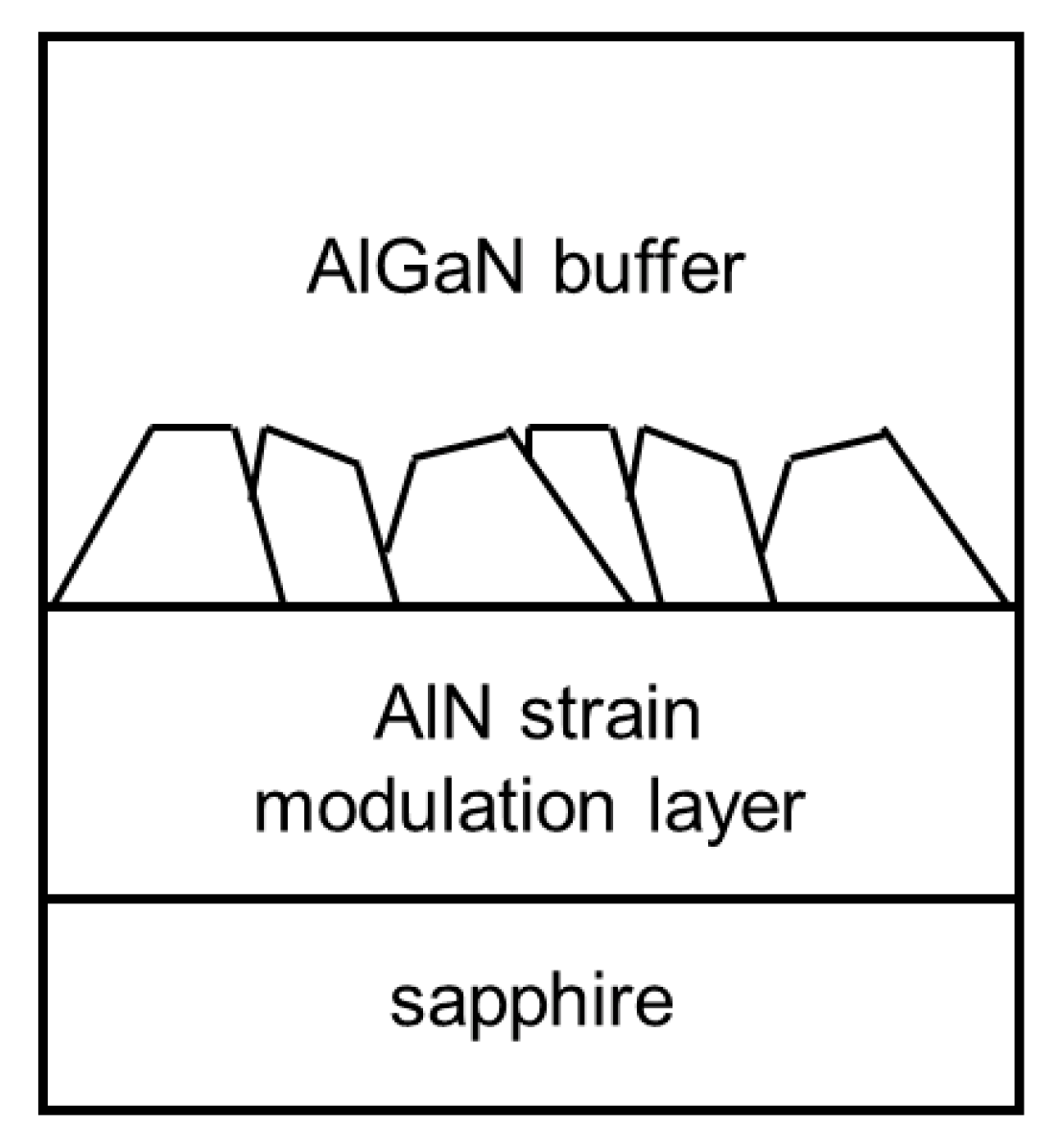
4.2. Mismatch Stress Relief

The growth model of AlGaN on the AlN strain modulation layer can be described by three stages: (i) nucleation; (ii) coalescence; and (iii) two-dimensional growth (2D growth); these are shown in Figure 4a [24,25]. Due to the large mismatch strain between AlN and AlGaN, deposited AlGaN will not form a flat surface, but first form a large number of small grains, which is called the nucleation stage [24]. The surface becomes rougher and rougher during stress relief through nucleation and grain growth. The in situ reflectance curve shows a drop at the nucleation stage. Then, at the coalescence stage, grains continue to grow and start to coalesce. Furthermore, the surface becomes smoother and the optical reflectance rises. Finally, the reflectance stops increasing and 2D growth of the AlGaN begins. If the mismatch strain is released adequately at the nucleation and coalescence stages, AlGaN will be relaxed in the beginning of 2D growth stage. Otherwise, the remaining stress will be released at the 2D growth stage by forming new dislocations, specifically, threading edge dislocations [26]. Strain relaxation will mainly cause the twist of (100) faces, which can be detected by the broadening of β(100) [27].
It is noted that the growth conditions of samples C, D, and E in Table 1, i.e., their source gas flow rates, are different. The XRD results of samples C, D, and E are different, as shown by Table 3. This indicates that the source gas flow rate can influence AlGaN’s β(100) of XRD. Among these three samples, sample C’s precursor flow rate is the lowest and that of E is the highest. When the flow rate is too high, the mismatch strain between AlN and AlGaN is unable to be released adequately during the nucleation and coalescence stages. As shown in Figure 4b, compared to sample C, the nucleation and coalescence stages of sample E are much shorter. The duration of the nucleation and coalescence stages of sample E is less than 20 min, whereas the duration of C is over 80 min. Moreover, sample E’s reflectance decrease during the nucleation stage is also less, which means that the mismatch strain relief may be not adequate at these stages. The remaining stress will be released at the 2D growth stage by the generation of a higher density of edge dislocations, which results in the highest AlGaN β(100) value of sample E among the three samples. Therefore, it is assumed that enhancing stress relief in nucleation and coalescence stages can decease the density of AlGaN edge dislocations.

4.3. Control of Aluminum Atom Migration Length

Another important quality index of AlGaN buffer is the surface roughness [28,29]. A smooth surface will actively contribute to the growth of the subsequent layer structure. This study found that appropriate restraint of the Al atom migration length improved the AlGaN surface. According to the AFM image results of samples C, D, and E, a higher precursor flow rate can yield a better surface. The roughness results also show that sample E has the flattest surface. A low source gas flow rate leads to a low AlGaN growth rate at the 2D growth stage. The growth rates for samples C, D, and E at the 2D growth stage were 1.45, 2.52, and 3.35 μm/h, respectively. Generally, a slower growth rate can increase the Al atom migration length and thus induce a flatter surface. An Al atom migration length that is too short will hinder step flow growth. However, even sample E, which has the faster growth rate among samples C, D, and E, had a clear step flow morphology. This indicates the Al atom migration length was enough for a good step flow growth mode in our study. In this case, increasing the Al atom migration length may no longer result in a flatter surface. Conversely, when the growth rate is too low, the migration distance of Al atoms on the surface will be too large, so the Al atom migration distance may be much higher than the separation between steps [30,31]. A step edge on the grown surface will be much more likely to interact with more atoms, which may be heterogeneously accumulated and induce a rougher surface [30]. Hence, reducing Al atom migration length appropriately may contribute to a smoother AlGaN surface.

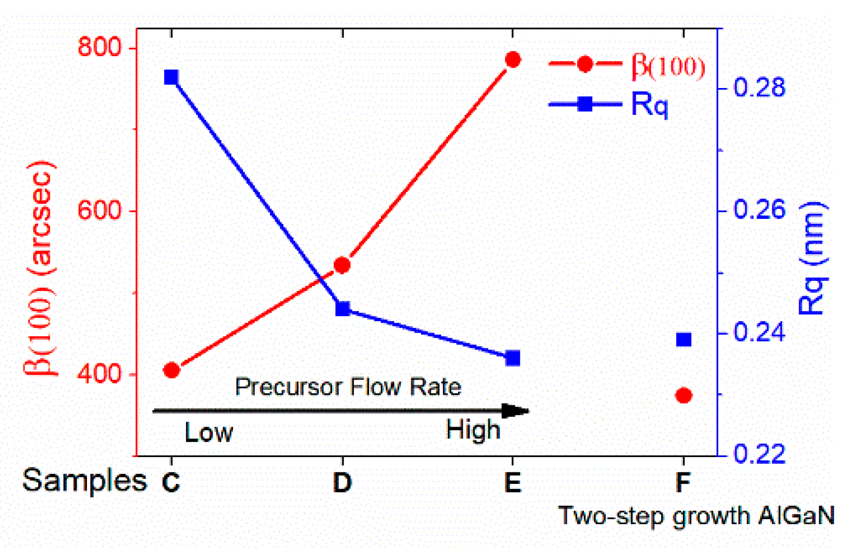
4.4. Two-Step Growth Method

To acquire an AlGaN buffer layer with high crystalline quality, three aspects need to be address, as discussed. Firstly, an additional AlGaN growth step is necessary in order to restrain the influence of gallium residues. Moreover, according to the discussions above, a low precursor flow rate can improve the stress relief in nucleation and coalescence stages, whereas a higher growth rate will reduce Al atom migration length. Hence, precursor flow rate plays an extremely important role in AlGaN quality, which can be clearly seen from Figure 5.
In order to simultaneously acquire both a low edge dislocation density and a flat surface, a two-step AlGaN growth method was designed and tested. As shown in Table 2, this method uses a low precursor flow rate in the nucleation and combination stages, and a higher flow rate in its 2D growth stage. At the beginning of AlGaN growth, a lower precursor flow rate causes longer nucleation and combination stages. The reflectance of sample F drops abruptly and then rises slowly, as shown in Figure 4b. The mismatch stress between the AlN strain modulation layer and the AlGaN buffer layer is adequately released. Then, a higher precursor flow rate is applied at the 2D growth stage. A higher growth rate can reduce the Al atom migration length and thus lead to a better AlGaN surface. The sample F’s XRD β(002) was 207 arcsec, its β(102) was 297 arcsec, and its β(100) was 374 arcsec. This result was also better than typical qualities for AlGaN layers grown on sapphire (366 arcsec for β(002) and 1023 arcsec for β(102)) [32]. These data of the XRD result are close to those of the AlGaN grown using a low gas precursor flow rate (sample C), representing low values of the dislocation densities. By comparison, sample F’s Rq was 0.239 nm and its Ra was 0.188 nm. These values are also relatively low, which means it has a surface quality similar to that of AlGaN layers grown using a high growth rate (such as samples D and E). Based on the two-step growth method, a AlGaN device buffer layer was grown having a low density of edge dislocations and a flat surface.

5. Conclusions

The mechanisms of AlGaN growth and the methods of crystalline quality improvement were studied. Gallium residues left in the MOCVD reactor chamber may influence the quality of the grown AlN strain modulation layer and the AlGaN device buffer layer. Passing TMAl in the reactor chamber during the temperature lifting process can reduce the influence of gallium residues. Furthermore, the problem can be also solved in another manner: by growing an additional AlGaN layer in the MOCVD reactor before the AlGaN buffer growth. In the paper, the effects of the stress relief and Al atom migration length on the AlGaN buffer are discussed. The stress relief in nucleation and coalescence stages can efficiently decrease the density of edge dislocations induced by strain relaxation in the 2D growth stage. By comparison, an appropriate restraint of Al atoms’ surface migration can improve the AlGaN surface. By adjusting the precursor flow rate, the stress relief process and Al atom migration length can be controlled. Hence, a two-step growth method is proposed, in which a low precursor flow rate is applied in nucleation and coalescence stages, and a higher flow rate is applied in the 2D growth stage. Using this two-step growth method, we acquired a high-quality AlGaN buffer layer having both a lower edge dislocation density and a flatter surface.

Supplementary Materials

The following supporting information can be downloaded at: https://www.mdpi.com/article/10.3390/cryst12081131/s1, Figure S1: The (105) RSM of samples A, B, C, D, E, and F; Table S1: The reciprocal space coordinates of AlGaN (105) RSM and the Al composition for the six samples.

Author Contributions

Conceptualization, B.W. and J.Y.; methodology, B.W. and J.Y.; software, Z.L.; validation, Y.Z. and Z.Z.; formal analysis, F.L.; investigation, P.C.; resources, D.Z.; data curation, B.W.; writing—original draft preparation, B.W.; writing—review and editing, B.W.; visualization, Z.L.; supervision, D.Z. and J.Y.; project administration, D.Z. and J.Y.; funding acquisition, D.Z. All authors have read and agreed to the published version of the manuscript.

Funding

This work was supported by Beijing Municipal Science & Technology Commission, Administrative Commission of Zhongguancun Science Park (Z211100004821001), National Natural Science Foundation of China (Grant Nos. 62034008, 62074142, 62074140, 61974162, 61904172, 61874175, 62127807, U21B2061), Key Research and Development Program of Jiangsu Province (BE2021008-1), Beijing Nova Program (Grant No. 202093), Strategic Priority Research Program of Chinese Academy of Sciences (Grant No. XDB43030101), Youth Innovation Promotion Association of Chinese Academy of Sciences (Grant No. 2019115), and Beijing Municipal Science and Technology Project (Grant No. Z211100007921022).

Institutional Review Board Statement

Not applicable.

Informed Consent Statement

Not applicable.

Data Availability Statement

The data that support the findings of this study are available from the corresponding author upon reasonable request.

Conflicts of Interest

The authors declare no conflict of interest.

References

  1. Susilo, N.; Enslin, J.; Sulmoni, L.; Guttmann, M.; Zeimer, U.; Wernicke, T.; Weyers, M.; Kneissl, M. Effect of the GaN:Mg Contact Layer on the Light-Output and Current-Voltage Characteristic of UVB LEDs. Phys. Status Solidi A 2018, 215, 1700643. [Google Scholar] [CrossRef]
  2. Hirayama, H.; Noguchi, N.; Fujikawa, S.; Norimatsu, J.; Kamata, N.; Takano, T.; Tsubaki, K. 222–282 nm AlGaN and InAlGaN Based Deep-UV LEDs Fabricated on High-Quality AlN Template; SPIE: Bellingham, WA, USA, 2009; Volume 7216. [Google Scholar]
  3. Maeda, N.; Jo, M.; Hirayama, H. Improving the Light-Extraction Efficiency of AlGaN DUV-LEDs by Using a Superlattice Hole Spreading Layer and an Al Reflector. Phys. Status Solidi A 2018, 215, 1700436. [Google Scholar] [CrossRef]
  4. Zetian, M.; Hieu Pham Trung, N.; Shaofei, Z.; Ashfiqua, T.C.; Md Golam, K.; Qi, W.; Ishiang, S. Phosphor-free InGaN/GaN/AlGaN core-shell dot-in-a-wire white light-emitting diodes. In Proceedings of the Light-Emitting Diodes: Materials, Devices, and Applications for Solid State Lighting XVIII, San Francisco, CA, USA, 27 February 2014. [Google Scholar]
  5. Guo, Y.; Yan, J.; Zhang, Y.; Wang, J.; Li, J. Enhancing the light extraction of AlGaN-based ultraviolet light-emitting diodes in the nanoscale. J. Nanophotonics 2018, 12, 043513. [Google Scholar] [CrossRef]
  6. Walter, J.; Cremer, T.; Miyagawa, K.; Tashiro, S. A new system for laser-UVA-microirradiation of living cells. J. Microsc. 2003, 209, 71–75. [Google Scholar] [CrossRef] [PubMed]
  7. Amano, H.; Collazo, R.; Santi, C.D.; Einfeldt, S.; Funato, M.; Glaab, J.; Hagedorn, S.; Hirano, A.; Hirayama, H.; Ishii, R.; et al. The 2020 UV Emitter Roadmap. J. Phys. D Appl. Phys. 2020, 53, 503001. [Google Scholar] [CrossRef]
  8. Li, D.B.; Jiang, K.; Sun, X.J.; Guo, C.L. AlGaN photonics: Recent advances in materials and ultraviolet devices. Adv. Opt. Photonics 2018, 10, 43–110. [Google Scholar] [CrossRef]
  9. Mohan, M.K.; Shim, S.K.; Lee, J.K.; Jang, N.; Lee, N.; Tawfik, W.Z. Optimized Aluminum Reflector for Enhancement of UVC Cathodoluminescence Based-AlGaN Materials with Carbon Nanotube Field Emitters. Molecules 2021, 26, 4025. [Google Scholar] [CrossRef]
  10. Kim, S.-B.; Bae, S.-B.; Ko, Y.-H.; Kim, D.C.; Nam, E.-S. Stimulated Emission with 349-nm Wavelength in GaN/AlGaN MQWs by Optical Pumping. Appl. Sci. Converg. Technol. 2017, 26, 79–85. [Google Scholar] [CrossRef]
  11. Tsuzuki, H.; Mori, F.; Takeda, K.; Ichikawa, T.; Iwaya, M.; Kamiyama, S.; Amano, H.; Akasaki, I.; Yoshida, H.; Kuwabara, M.; et al. High-performance UV emitter grown on high-crystalline-quality AlGaN underlying layer. Phys. Status Solidi A 2009, 206, 1199–1204. [Google Scholar] [CrossRef]
  12. Iida, K.; Kawashima, T.; Miyazaki, A.; Kasugai, H.; Mishima, S.; Honshio, A.; Miyake, Y.; Iwaya, M.; Kamiyama, S.; Amano, H.; et al. Laser diode of 350.9 nm wavelength grown on sapphire substrate by MOVPE. J. Cryst. Growth 2004, 272, 270–273. [Google Scholar] [CrossRef]
  13. Iida, K.; Kawashima, T.; Miyazaki, A.; Kasugai, H.; Mishima, S.; Honshio, A.; Miyake, Y.; Iwaya, M.; Kamiyama, S.; Amano, H.; et al. 350.9 nm UV Laser Diode Grown on Low-Dislocation-Density AlGaN. Jpn. J. Appl. Phys. 2004, 43, L499–L500. [Google Scholar] [CrossRef]
  14. Sato, K.; Yasue, S.; Ogino, Y.; Iwaya, M.; Takeuchi, T.; Kamiyama, S.; Akasaki, I. Electrical properties of relaxed p-GaN/p-AlGaN superlattices and their application in ultraviolet-B light-emitting devices. Jpn. J. Appl. Phys. 2019, 58, SC1016. [Google Scholar] [CrossRef]
  15. Iwaya, M.; Terao, S.; Hayashi, N.; Kashima, T.; Amano, H.; Akasaki, I. Realization of crack-free and high-quality thick AlxGa1−xN for UV optoelectronics using low-temperature interlayer. Appl. Surf. Sci. 2000, 159, 405–413. [Google Scholar] [CrossRef]
  16. Omori, T.; Ishizuka, S.; Tanaka, S.; Yasue, S.; Sato, K.; Ogino, Y.; Teramura, S.; Yamada, K.; Iwayama, S.; Miyake, H.; et al. Internal loss of AlGaN-based ultraviolet-B band laser diodes with p-type AlGaN cladding layer using polarization doping. Appl. Phys. Express 2020, 13, 071008. [Google Scholar] [CrossRef]
  17. Sato, K.; Yasue, S.; Yamada, K.; Tanaka, S.; Omori, T.; Ishizuka, S.; Teramura, S.; Ogino, Y.; Iwayama, S.; Miyake, H.; et al. Room-temperature operation of AlGaN ultraviolet-B laser diode at 298 nm on lattice-relaxed Al0.6Ga0.4N/AlN/sapphire. Appl. Phys. Express 2020, 13, 5. [Google Scholar] [CrossRef]
  18. Tanaka, S.; Ogino, Y.; Yamada, K.; Omori, T.; Ogura, R.; Teramura, S.; Shimokawa, M.; Ishizuka, S.; Yabutani, A.; Iwayama, S.; et al. AlGaN-based UV-B laser diode with a high optical confinement factor. Appl. Phys. Lett. 2021, 118, 163504. [Google Scholar] [CrossRef]
  19. Pereira, S.; Correia, M.R.; Pereira, E.; O’Donnell, K.P.; Alves, E.; Sequeira, A.D.; Franco, N.; Watson, I.M.; Deatcher, C.J. Strain and composition distributions in wurtzite InGaN/GaN layers extracted from x-ray reciprocal space mapping. Appl. Phys. Lett. 2002, 80, 3913–3915. [Google Scholar] [CrossRef]
  20. Schuster, M.; Gervais, P.O.; Jobst, B.; Hösler, W.; Averbeck, R.; Riechert, H.; Iberl, A.; Stömmer, R. Determination of the chemical composition of distorted InGaN/GaN heterostructures from x-ray diffraction data. J. Phys. D Appl. Phys. 1999, 32, A56–A60. [Google Scholar] [CrossRef]
  21. Zhang, J.C.; Zhao, D.G.; Wang, J.F.; Wang, Y.T.; Chen, J.; Liu, J.P.; Yang, H. The influence of AlN buffer layer thickness on the properties of GaN epilayer. J. Cryst. Growth 2004, 268, 24–29. [Google Scholar] [CrossRef]
  22. Ran, J.; Wang, X.; Hu, G.; Wang, J.; Li, J.; Wang, C.; Zeng, Y.; Li, J. Study on Mg memory effect in npn type AlGaN/GaN HBT structures grown by MOCVD. Microelectron. J. 2006, 37, 583–585. [Google Scholar] [CrossRef]
  23. Zhang, Y.; Yang, J.; Zhao, D.; Liang, F.; Chen, P.; Liu, Z. The deterioration of AlN quality caused by residual gallium in the MOCVD reaction chamber. Jpn. J. Appl. Phys. 2022, 61, 070905. [Google Scholar] [CrossRef]
  24. Teramura, S.; Kawase, Y.; Sakuragi, Y.; Iwayama, S.; Iwaya, M.; Takeuchi, T.; Kamiyama, S.; Akasaki, I.; Miyake, H. High Crystallinity and Highly Relaxed Al0.60Ga0.40N Films Using Growth Mode Control Fabricated on a Sputtered AlN Template with High-Temperature Annealing. Phys. Status Solidi A 2020, 217, 1900868. [Google Scholar] [CrossRef]
  25. Kawase, Y.; Ikeda, S.; Sakuragi, Y.; Yasue, S.; Iwayama, S.; Iwaya, M.; Takeuchi, T.; Kamiyama, S.; Akasaki, I.; Miyake, H. Ultraviolet-B band lasers fabricated on highly relaxed thick Al0.55Ga0.45N films grown on various types of AlN wafers. Jpn. J. Appl. Phys. 2019, 58, SC1052. [Google Scholar] [CrossRef]
  26. Ji, Q.; Li, L.; Zhang, W.; Wang, J.; Liu, P.; Xie, Y.; Yan, T.; Yang, W.; Chen, W.; Hu, X. Dislocation Reduction and Stress Relaxation of GaN and InGaN Multiple Quantum Wells with Improved Performance via Serpentine Channel Patterned Mask. ACS Appl. Mater. Interfaces 2016, 8, 21480–21489. [Google Scholar] [CrossRef]
  27. Grundmann, M. Defects. In The Physics of Semiconductors: An Introduction Including Nanophysics and Applications; Springer: Berlin/Heidelberg, Germany, 2010; pp. 73–102. [Google Scholar]
  28. Ahaitouf, A.; Ougazzaden, A.; Troadec, D.; Orsal, G.; Patriarche, G.; Salvestrini, J.P.; Pantzas, K.; Gautier, S.; Moudakir, T.; Gmili, Y.E. Characteristics of the surface microstructures in thick InGaN layers on GaN. Opt. Mater. Express 2013, 3, 1111–1118. [Google Scholar]
  29. Svensk, O.; Suihkonen, S.; Sintonen, S.; Kopylov, O.; Shirazi, R.; Lipsanen, H.; Sopanen, M.; Kardynal, B.E. MOCVD growth and characterization of near-surface InGaN/GaN single quantum wells for non-radiative coupling of optical excitations. Phys. Status Solidi C 2012, 9, 1667–1669. [Google Scholar] [CrossRef]
  30. Zhang, Y.H.; Yang, J.; Zhao, D.G.; Liang, F.; Chen, P.; Liu, Z.S. Adjustment of Al atom migration ability and its effect on the surface morphology of AlN grown on sapphire by metal-organic chemical vapor deposition. Semicond. Sci. Technol. 2021, 36, 105010. [Google Scholar] [CrossRef]
  31. Banal, R.G.; Funato, M.; Kawakami, Y. Initial nucleation of AlN grown directly on sapphire substrates by metal-organic vapor phase epitaxy. Appl. Phys. Lett. 2008, 92, 241905. [Google Scholar] [CrossRef]
  32. Zhang, L.; Yan, J.; Wu, Q.; Guo, Y.; Yang, C.; Wei, T.; Liu, Z.; Yuan, G.; Wei, X.; Zhao, L.; et al. Improved crystalline quality of Al-rich n-AlGaN by regrowth on nanoporous template fabricated by electrochemical etching. J. Nanophotonics 2018, 12, 043509. [Google Scholar] [CrossRef]
Figure 1. The schematic diagram of the sample structure in the vertical direction.
Crystals 12 01131 g001
Figure 2. The 5 × 5 μm AFM images of samples (AF).
Crystals 12 01131 g002
Figure 3. The (002) (a) and (102) (b) ω scan of samples A, B, C, D, E, and F.
Crystals 12 01131 g003
Figure 4. (a) The schematic diagram of an in situ reflectance curve divided in 3 parts in the initial stage of AlGaN growth. (b) The in situ 633 nm reflectance curves of samples C, D, E, and F.
Crystals 12 01131 g004
Figure 5. The relationship between precursor flow rate and AlGaN crystalline qualities.
Crystals 12 01131 g005
Table 1. The growth parameters of AlGaN samples A, B, C, D, and E.
SamplePre-TMAl
(sccm)
TMAl
(sccm)
TMGa
(sccm)
NH3
(sccm)
An Additional AlGaN GrowthAluminum
Composition
A127.534.73000No18.2%
B527.534.73000No19.0%
C027.534.73000Yes17.6%
D041.052.04500Yes16.5%
E055.069.46000Yes16.1%
Table 2. The growth parameters of sample F.
Growth StageFlow Rate (sccm)
TMAlTMGaNH3
Nucleation27.534.73000
Coalescence27.534.73000
2D Growth41.052.04500
Pre-TMAl
(sccm)
0An Additional AlGaN GrowthYesAluminum
Composition
16.8%
Table 3. The crystalline quality indexes of 6 AlGaN samples.
SampleAFM Roughness (nm)AlGaN XRD FWHM (arcsec)
RqRa(002)(102)(100)
A0.6220.4781489451373
B0.4140.317152594854
C0.2820.216206315405
D0.2440.194149381534
E0.2360.188153549786
F0.2390.188207297374
Publisher’s Note: MDPI stays neutral with regard to jurisdictional claims in published maps and institutional affiliations.

