
Development of Solution-Processed Perovskite Semiconductors Lasers


Abstract
:1. Introduction
2. Perovskite Semiconductor
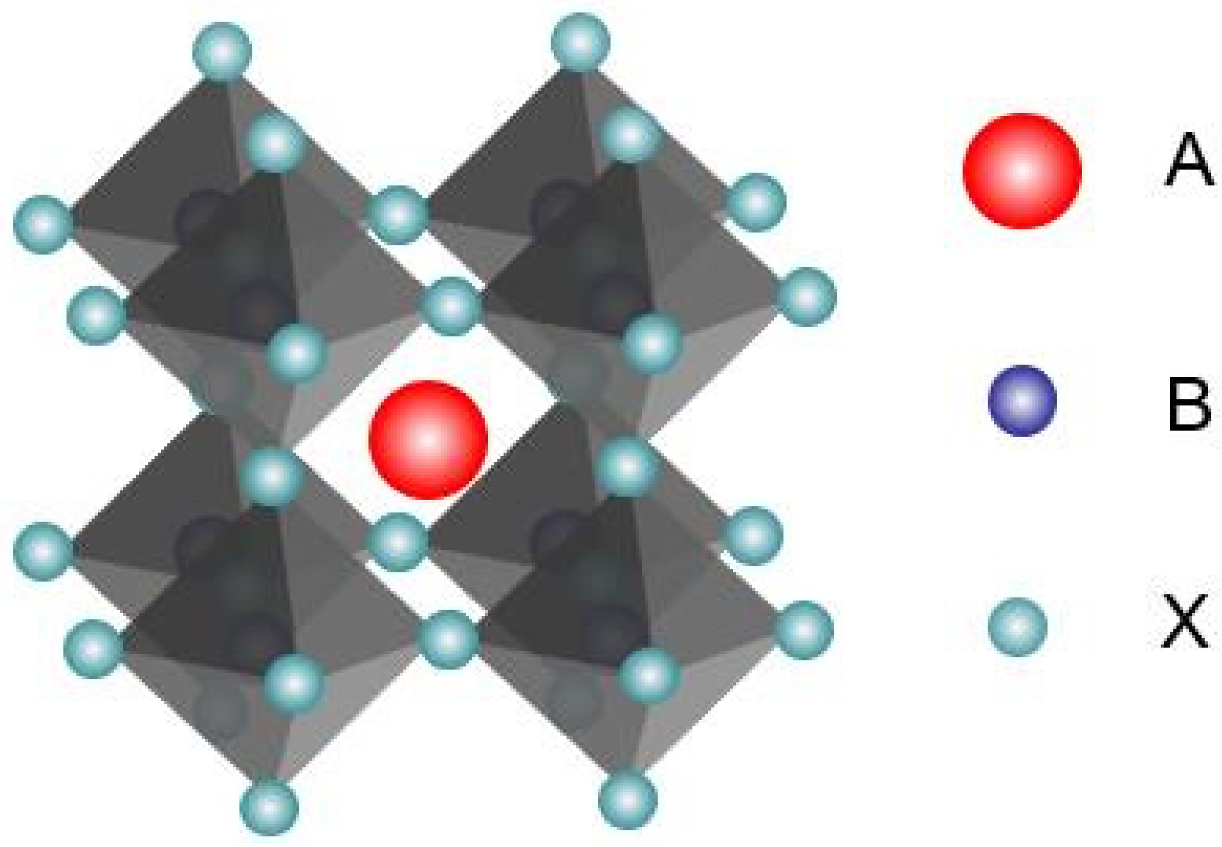
2.1. Crystal Structure
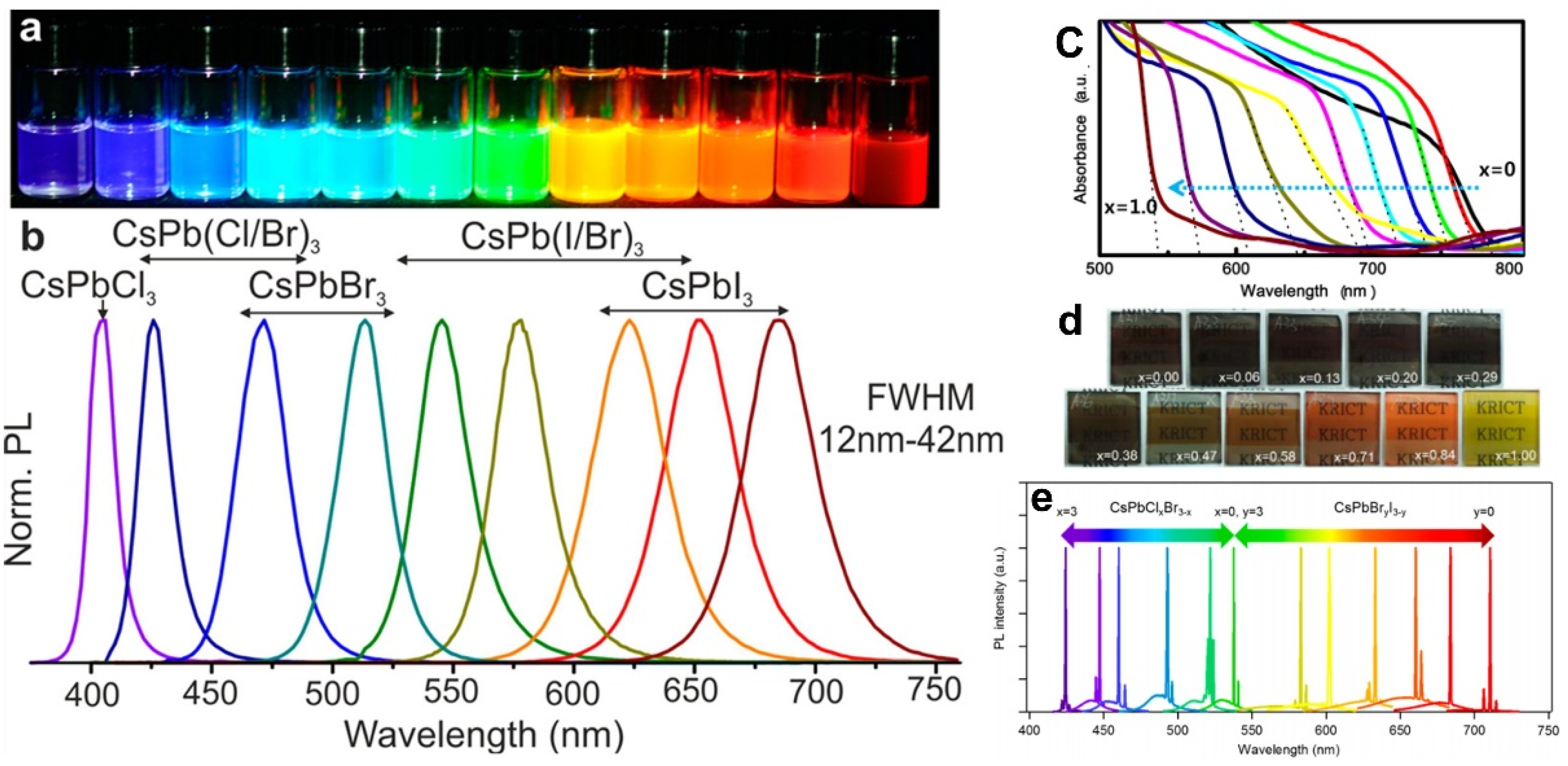
2.2. Luminescence Properties
2.3. Gain Properties
2.4. Carrier Dynamics
2.5. Stability
3. Perovskite Semiconductor Lasers
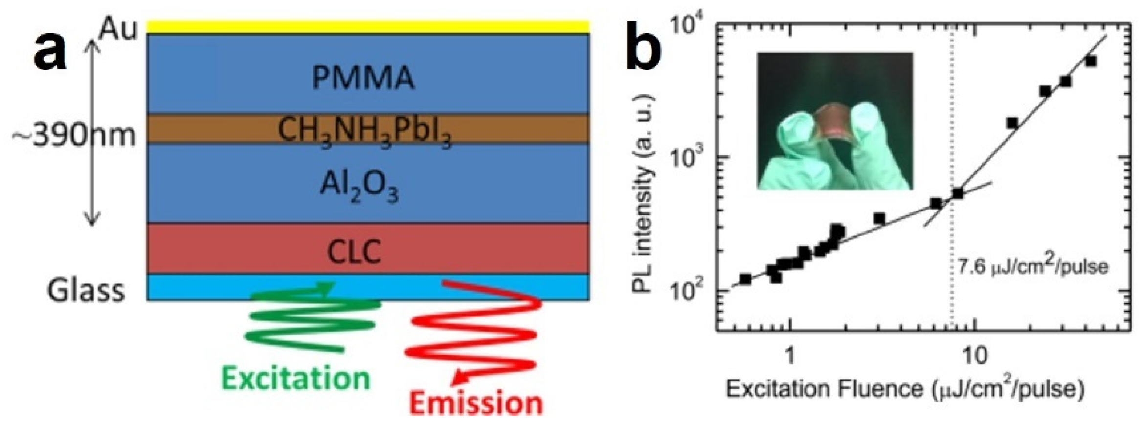
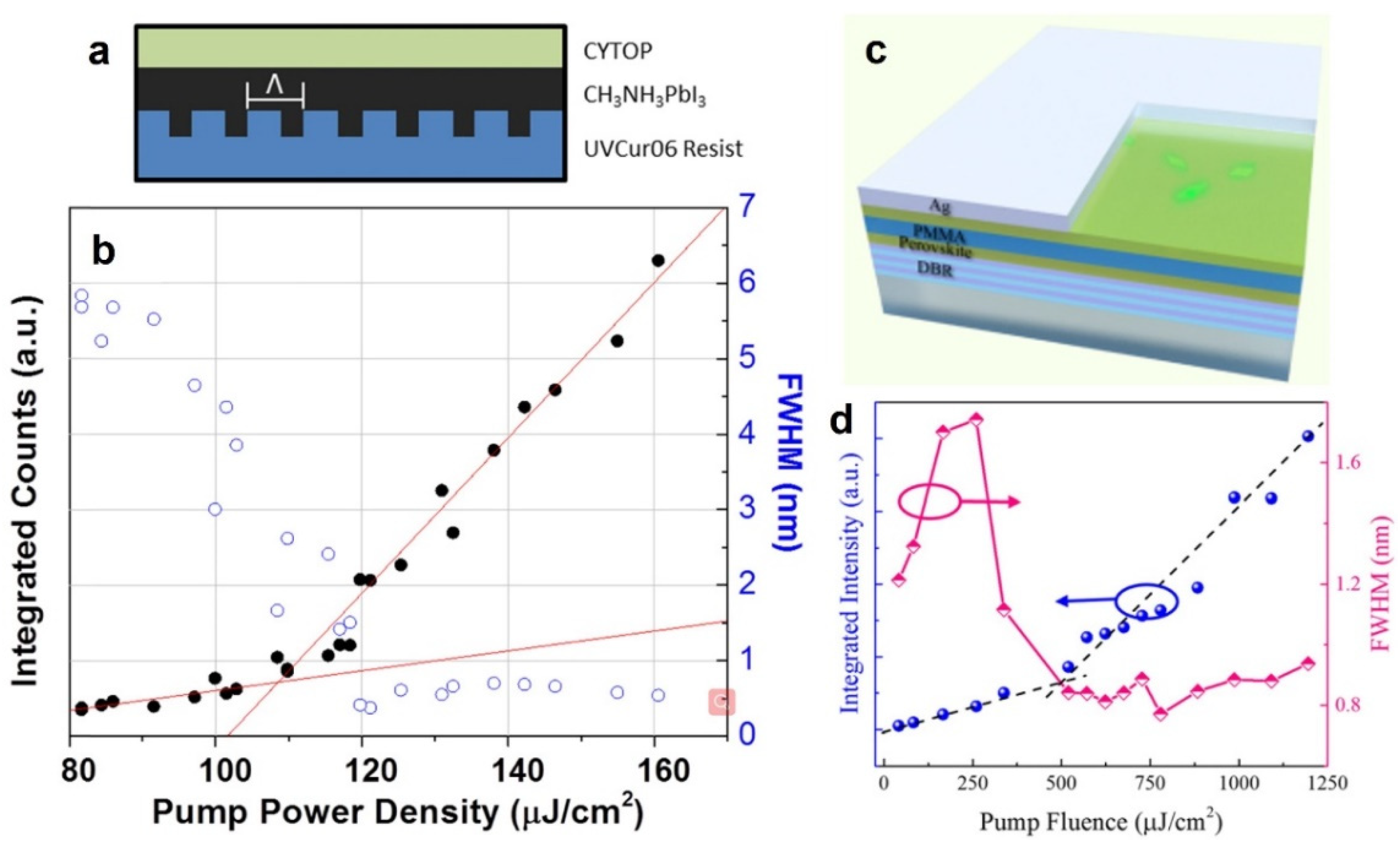
3.1. Polycrystalline Thin-Film Perovskite Lasers
3.2. Single Crystals Perovskite Thin Film Lasers
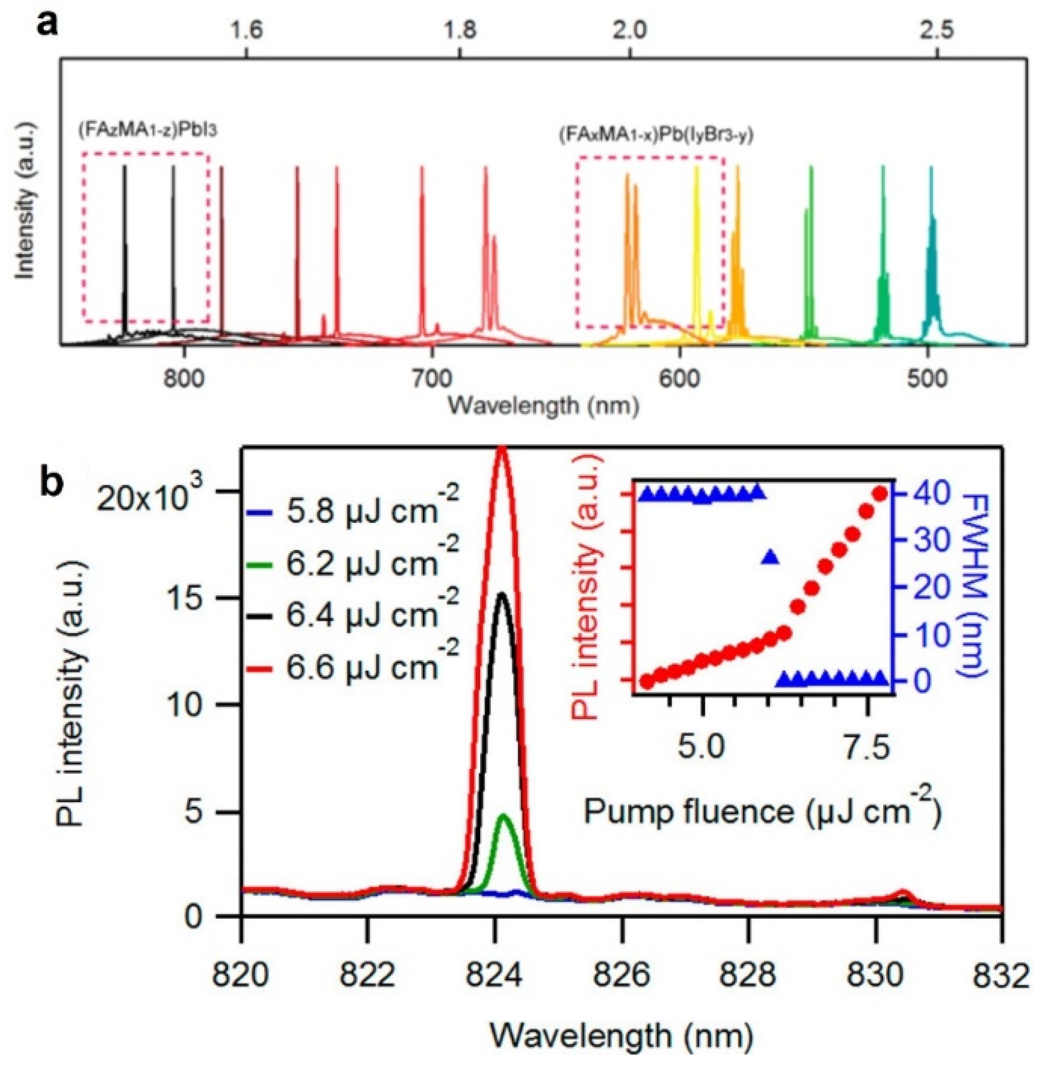
3.3. Single Crystals Perovskite Nanowires Lasers
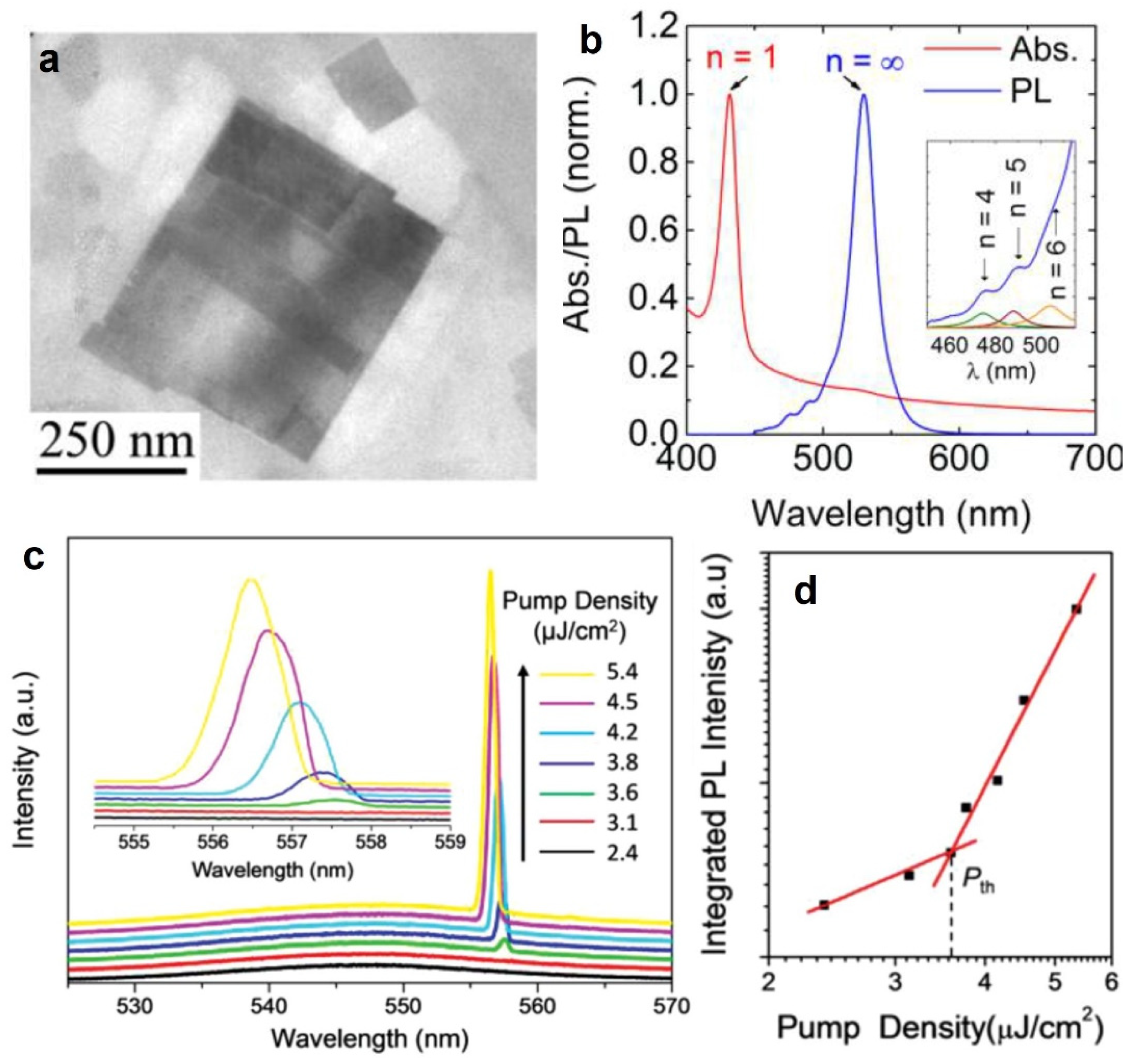
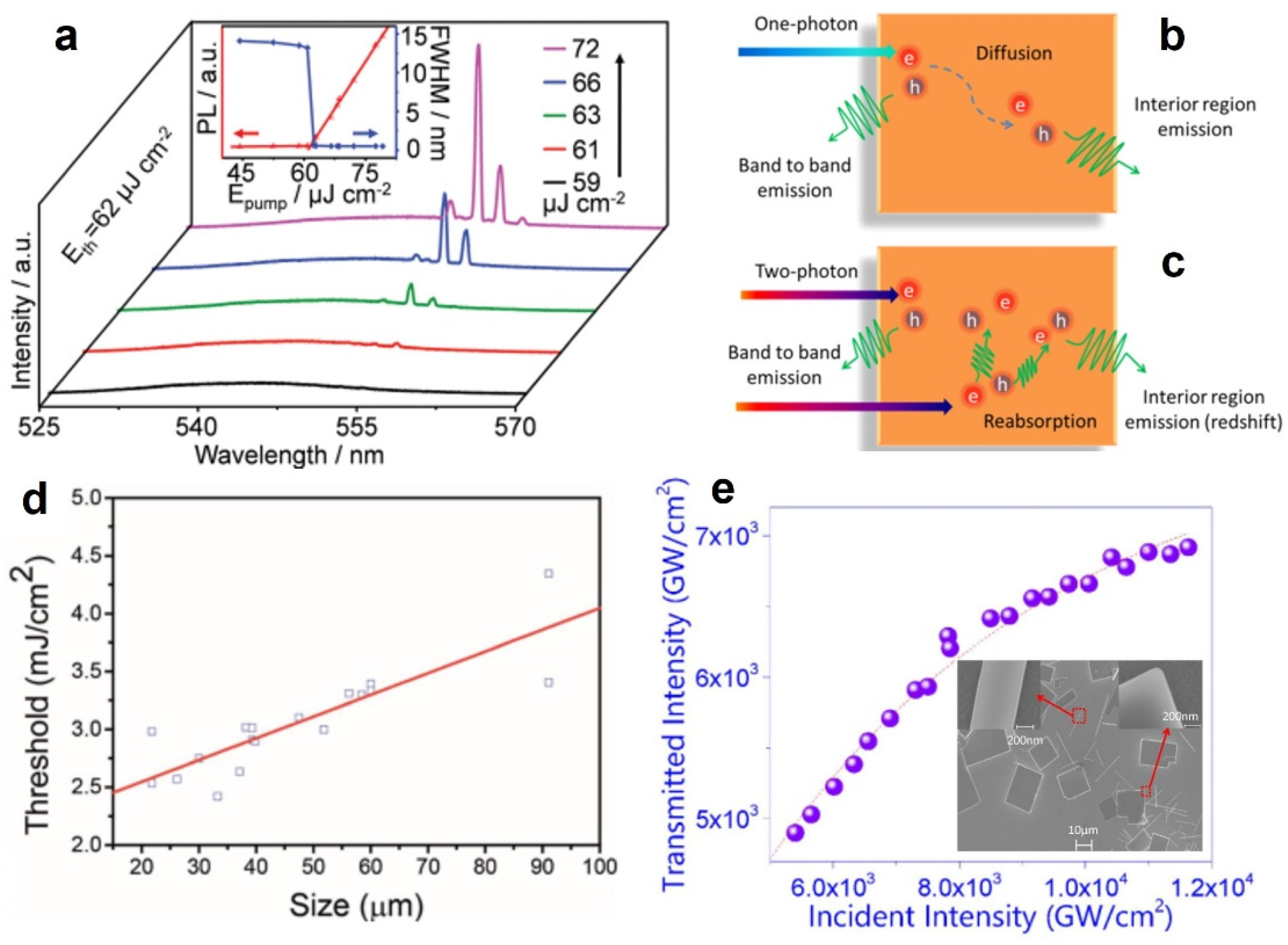
3.4. Single Crystals Perovskite Microplates/Nanoplatelets Lasers
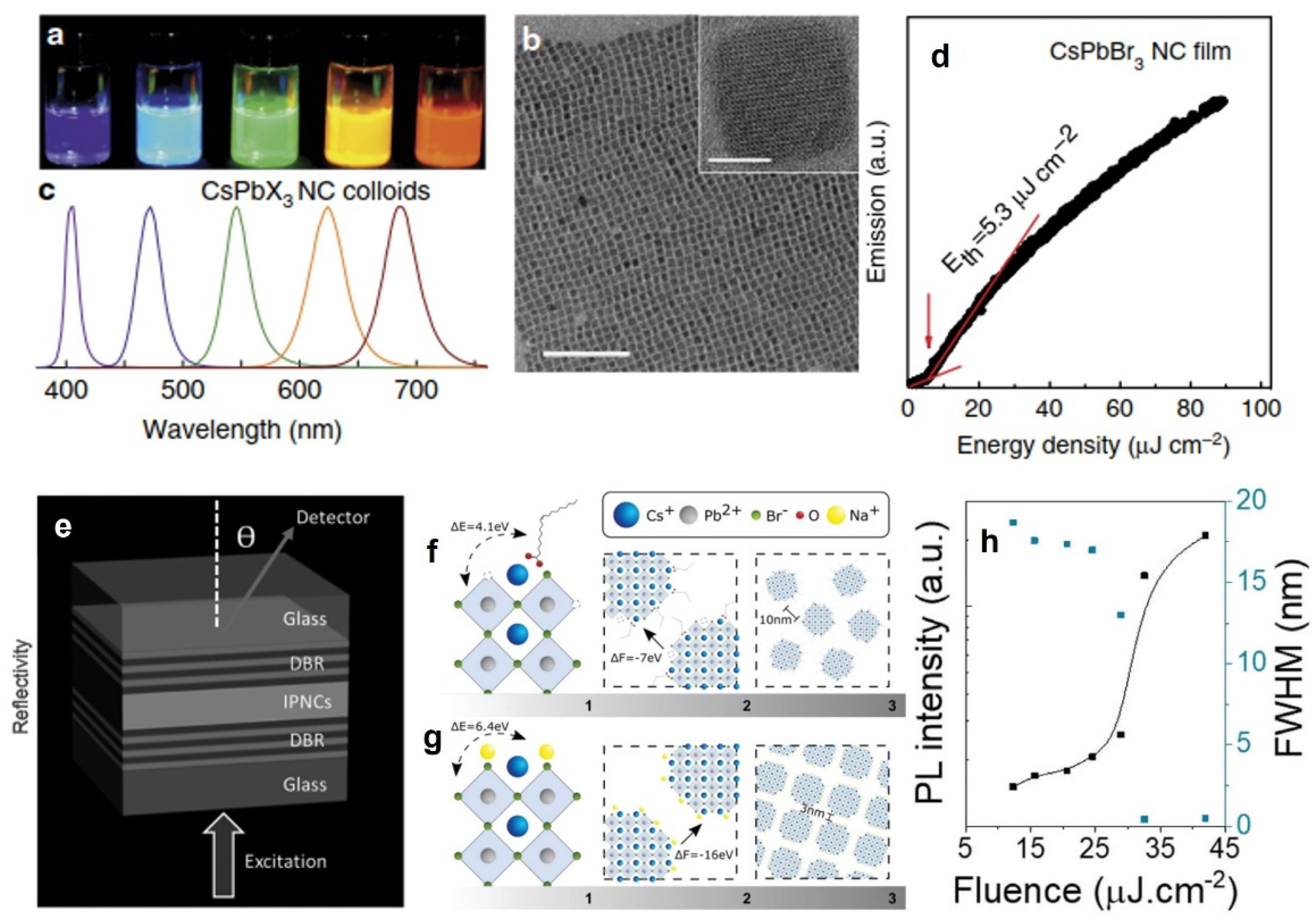
3.5. Perovskite Quantum Dots Lasers
3.6. Others
4. Conclusions
Author Contributions
Funding
Institutional Review Board Statement
Informed Consent Statement
Data Availability Statement
Acknowledgments
Conflicts of Interest
References
- Hall, R.N.; Fenner, G.E.; Kingsley, J.; Soltys, T.; Carlson, R. Coherent light emission from GaAs junctions. Phys. Rev. Lett. 1962, 9, 366. [Google Scholar] [CrossRef]
- Nathan, M.I.; Dumke, W.P.; Burns, G.; Dill, F.H., Jr.; Lasher, G. Stimulated emission of radiation from GaAs p-n junctions. Appl. Phys. Lett. 1962, 1, 62–64. [Google Scholar] [CrossRef]
- Xia, H.; Hu, C.; Chen, T.; Hu, D.; Zhang, M.; Xie, K. Advances in Conjugated Polymer Lasers. Polymers 2019, 11, 443. [Google Scholar] [CrossRef] [PubMed]
- McGehee, M.D.; Heeger, A.J. Semiconducting (conjugated) polymers as materials for solid-state lasers. Adv. Mater. 2000, 12, 1655–1668. [Google Scholar] [CrossRef]
- Zhao, J.; Yan, Y.; Zhao, Y.; Yao, J. Research progress on organic micro/nanoscale lasers. Sci. Sin. Chim. 2018, 48, 127–142. [Google Scholar] [CrossRef]
- Clark, J.; Lanzani, G. Organic photonics for communications. Nat. Photonics 2010, 4, 438–446. [Google Scholar] [CrossRef]
- de Arquer, F.P.G.; Armin, A.; Meredith, P.; Sargent, E.H. Solution-processed semiconductors for next-generation photodetectors. Nat. Rev. Mater. 2017, 2, 16100. [Google Scholar] [CrossRef]
- Zhang, C.; Yan, Y.; Zhao, Y.S.; Yao, J. From molecular design and materials construction to organic nanophotonic devices. Acc. Chem. Res. 2014, 47, 3448–3458. [Google Scholar] [CrossRef]
- Gierschner, J.; Varghese, S.; Park, S.Y. Organic single crystal lasers: A materials view. Adv. Opt. Mater. 2016, 4, 348–364. [Google Scholar] [CrossRef]
- Yan, Y.; Zhao, Y.S. Organic nanophotonics: From controllable assembly of functional molecules to low-dimensional materials with desired photonic properties. Chem. Soc. Rev. 2014, 43, 4325–4340. [Google Scholar] [CrossRef]
- Fang, H.H.; Yang, J.; Feng, J.; Yamao, T.; Hotta, S.; Sun, H.B. Functional organic single crystals for solid-state laser applications. Laser Photonics Rev. 2014, 8, 687–715. [Google Scholar] [CrossRef]
- Sohler, W.; Rue, R. Organic solid-state integrated amplifiers and lasers. Laser Photonics Rev. 2012, 6, 419–462. [Google Scholar]
- Li, Y.J.; Yan, Y.; Zhao, Y.S.; Yao, J. Construction of Nanowire Heterojunctions: Photonic Function-Oriented Nanoarchitectonics. Adv. Mater. 2016, 28, 1319–1326. [Google Scholar] [CrossRef] [PubMed]
- Zhang, W.; Yao, J.; Zhao, Y.S. Organic micro/nanoscale lasers. Acc. Chem. Res. 2016, 49, 1691–1700. [Google Scholar] [CrossRef] [PubMed]
- Jung, H.; Ahn, N.; Klimov, V.I. Prospects and challenges of colloidal quantum dot laser diodes. Nat. Photonics 2021, 15, 643–655. [Google Scholar] [CrossRef]
- Fan, F.; Voznyy, O.; Sabatini, R.P.; Bicanic, K.T.; Adachi, M.M.; McBride, J.R.; Reid, K.R.; Park, Y.-S.; Li, X.; Jain, A. Continuous-wave lasing in colloidal quantum dot solids enabled by facet-selective epitaxy. Nature 2017, 544, 75–79. [Google Scholar] [CrossRef] [PubMed]
- Lim, J.; Park, Y.-S.; Klimov, V.I. Optical gain in colloidal quantum dots achieved with direct-current electrical pumping. Nat. Mater. 2018, 17, 42–49. [Google Scholar] [CrossRef]
- Park, Y.-S.; Roh, J.; Diroll, B.T.; Schaller, R.D.; Klimov, V.I. Colloidal quantum dot lasers. Nat. Rev. Mater. 2021, 6, 382–401. [Google Scholar] [CrossRef]
- Roh, J.; Park, Y.-S.; Lim, J.; Klimov, V.I. Optically pumped colloidal-quantum-dot lasing in LED-like devices with an integrated optical cavity. Nat. Commun. 2020, 11, 1–10. [Google Scholar] [CrossRef]
- Whitworth, G.L.; Harwell, J.R.; Miller, D.N.; Hedley, G.J.; Zhang, W.; Snaith, H.J.; Turnbull, G.A.; Samuel, I.D.W. Nanoimprinted distributed feedback lasers of solution processed hybrid perovskites. Opt. Express 2016, 24, 23677–23684. [Google Scholar] [CrossRef]
- Zhai, W.; Tian, C.; Yuan, K.; Ge, C.; Zhao, S.; Yu, H.; Li, Y.; Chen, W.; Ran, G. Optically pumped lasing of segregated quasi-2D perovskite microcrystals in vertical microcavity at room temperature. Appl. Phys. Lett. 2019, 114, 131107. [Google Scholar] [CrossRef]
- Zhu, H.; Fu, Y.; Meng, F.; Wu, X.; Gong, Z.; Ding, Q.; Gustafsson, M.V.; Trinh, M.T.; Jin, S.; Zhu, X. Lead halide perovskite nanowire lasers with low lasing thresholds and high quality factors. Nat. Mater. 2015, 14, 636–642. [Google Scholar] [CrossRef] [PubMed]
- Xing, G.; Mathews, N.; Lim, S.S.; Yantara, N.; Liu, X.; Sabba, D.; Grätzel, M.; Mhaisalkar, S.; Sum, T.C. Low-temperature solution-processed wavelength-tunable perovskites for lasing. Nat. Mater. 2014, 13, 476–480. [Google Scholar] [CrossRef] [PubMed]
- Yakunin, S.; Protesescu, L.; Krieg, F.; Bodnarchuk, M.I.; Nedelcu, G.; Humer, M.; De Luca, G.; Fiebig, M.; Heiss, W.; Kovalenko, M.V. Low-threshold amplified spontaneous emission and lasing from colloidal nanocrystals of caesium lead halide perovskites. Nat. Commun. 2015, 6, 1–9. [Google Scholar]
- Zhang, Q.; Ha, S.T.; Liu, X.; Sum, T.C.; Xiong, Q. Room-temperature near-infrared high-Q perovskite whispering-gallery planar nanolasers. Nano Lett. 2014, 14, 5995–6001. [Google Scholar] [CrossRef]
- Sutherland, B.R.; Hoogland, S.; Adachi, M.M.; Wong, C.T.; Sargent, E.H. Conformal organohalide perovskites enable lasing on spherical resonators. ACS Nano 2014, 8, 10947–10952. [Google Scholar] [CrossRef]
- Liao, Q.; Hu, K.; Zhang, H.; Wang, X.; Yao, J.; Fu, H. Perovskite microdisk microlasers self-assembled from solution. Adv. Mater. 2015, 27, 3405–3410. [Google Scholar] [CrossRef]
- Dhanker, R.; Brigeman, A.; Larsen, A.; Stewart, R.; Asbury, J.B.; Giebink, N.C. Random lasing in organo-lead halide perovskite microcrystal networks. Appl. Phys. Lett. 2014, 105, 151112. [Google Scholar] [CrossRef]
- Protesescu, L.; Yakunin, S.; Bodnarchuk, M.I.; Krieg, F.; Caputo, R.; Hendon, C.H.; Yang, R.X.; Walsh, A.; Kovalenko, M.V. Nanocrystals of cesium lead halide perovskites (CsPbX3, X= Cl, Br, and I): Novel optoelectronic materials showing bright emission with wide color gamut. Nano Lett. 2015, 15, 3692–3696. [Google Scholar] [CrossRef]
- Huang, L.-y.; Lambrecht, W.R. Electronic band structure, phonons, and exciton binding energies of halide perovskites CsSnCl 3, CsSnBr 3, and CsSnI 3. Phys. Rev. B 2013, 88, 165203. [Google Scholar] [CrossRef]
- Noh, J.H.; Im, S.H.; Heo, J.H.; Mandal, T.N.; Seok, S.I. Chemical management for colorful, efficient, and stable inorganic–organic hybrid nanostructured solar cells. Nano Lett. 2013, 13, 1764–1769. [Google Scholar] [CrossRef]
- Fu, Y.; Zhu, H.; Stoumpos, C.C.; Ding, Q.; Wang, J.; Kanatzidis, M.G.; Zhu, X.; Jin, S. Broad wavelength tunable robust lasing from single-crystal nanowires of cesium lead halide perovskites (CsPbX3, X= Cl, Br, I). ACS Nano 2016, 10, 7963–7972. [Google Scholar] [CrossRef] [PubMed]
- Jiang, Y.; Wang, X.; Pan, A. Properties of excitons and photogenerated charge carriers in metal halide perovskites. Adv. Mater. 2019, 31, 1806671. [Google Scholar] [CrossRef] [PubMed]
- Sutherland, B.R.; Hoogland, S.; Adachi, M.M.; Kanjanaboos, P.; Wong, C.T.; McDowell, J.J.; Xu, J.; Voznyy, O.; Ning, Z.; Houtepen, A.J. Perovskite thin films via atomic layer deposition. Adv. Mater. 2015, 27, 53–58. [Google Scholar] [CrossRef] [PubMed]
- Gao, W.; Yu, S.F. Reality or fantasy-Perovskite semiconductor laser diodes. Ecomat 2021, 3, e12077. [Google Scholar] [CrossRef]
- Shi, D.; Adinolfi, V.; Comin, R.; Yuan, M.; Alarousu, E.; Buin, A.; Chen, Y.; Hoogland, S.; Rothenberger, A.; Katsiev, K. Low trap-state density and long carrier diffusion in organolead trihalide perovskite single crystals. Science 2015, 347, 519–522. [Google Scholar] [CrossRef]
- Frost, J.M. Calculating polaron mobility in halide perovskites. Phys. Rev. B 2017, 96, 195202. [Google Scholar] [CrossRef]
- He, Y.; Galli, G. Perovskites for solar thermoelectric applications: A first principle study of CH3NH3AI3 (A= Pb and Sn). Chem. Mater. 2014, 26, 5394–5400. [Google Scholar] [CrossRef]
- Ye, T.; Wang, X.; Li, X.; Yan, A.Q.; Ramakrishna, S.; Xu, J. Ultra-high Seebeck coefficient and low thermal conductivity of a centimeter-sized perovskite single crystal acquired by a modified fast growth method. J. Mater. Chem. C 2017, 5, 1255–1260. [Google Scholar] [CrossRef]
- Pisoni, A.; Jacimovic, J.; Barisic, O.S.; Spina, M.; Gaál, R.; Forró, L.; Horváth, E. Ultra-low thermal conductivity in organic–inorganic hybrid perovskite CH3NH3PbI3. J. Phys. Chem. Lett. 2014, 5, 2488–2492. [Google Scholar] [CrossRef]
- Yang, A.; Bai, M.; Bao, X.; Wang, J.; Zhang, W. Investigation of Optical and Dielectric Constants of Organic-InorganicCH3NH3PbI3 Perovskite Thin Films. J. Nanomed. Nanotechnol. 2016, 7, 5–9. [Google Scholar]
- Kang, Y.; Han, S. Intrinsic carrier mobility of cesium lead halide perovskites. Phys. Rev. Appl. 2018, 10, 044013. [Google Scholar] [CrossRef]
- Yang, Z.; Xu, Q.; Wang, X.; Lu, J.; Wang, H.; Li, F.; Zhang, L.; Hu, G.; Pan, C. Large and ultrastable all-inorganic CsPbBr3 monocrystalline films: Low-temperature growth and application for high-performance photodetectors. Adv. Mater. 2018, 30, 1802110. [Google Scholar] [CrossRef] [PubMed]
- Ahmad, M.; Rehman, G.; Ali, L.; Shafiq, M.; Iqbal, R.; Ahmad, R.; Khan, T.; Jalali-Asadabadi, S.; Maqbool, M.; Ahmad, I. Structural, electronic and optical properties of CsPbX3 (X = Cl, Br, I) for energy storage and hybrid solar cell applications. J. Alloys. Compd. 2017, 705, 828–839. [Google Scholar] [CrossRef]
- Li, C.; Wang, A.; Deng, X.; Wang, S.; Yuan, Y.; Ding, L.; Hao, F. Insights into ultrafast carrier dynamics in perovskite thin films and solar cells. ACS Photonics 2020, 7, 1893–1907. [Google Scholar] [CrossRef]
- Stranks, S.D.; Burlakov, V.M.; Leijtens, T.; Ball, J.M.; Goriely, A.; Snaith, H.J. Recombination kinetics in organic-inorganic perovskites: Excitons, free charge, and subgap states. Phys. Rev. Appl. 2014, 2, 034007. [Google Scholar] [CrossRef]
- Yamada, Y.; Nakamura, T.; Endo, M.; Wakamiya, A.; Kanemitsu, Y. Photocarrier recombination dynamics in perovskite CH3NH3PbI3 for solar cell applications. J. Am. Chem. Soc. 2014, 136, 11610–11613. [Google Scholar] [CrossRef]
- Tian, J. Investigation of Pulsed Lasing Properties and Mechanisms in Lead-Based Perovskite Micro/Nano-Structures; East China Normal University: Shanghai, China, 2021. [Google Scholar]
- Boyd, C.C.; Cheacharoen, R.; Leijtens, T.; McGehee, M.D. Understanding Degradation Mechanisms and Improving Stability of Perovskite Photovoltaics. Chem. Rev. 2019, 119, 3418–3451. [Google Scholar] [CrossRef]
- Wei, Y.; Cheng, Z.; Lin, J. An overview on enhancing the stability of lead halide perovskite quantum dots and their applications in phosphor-converted LEDs. Chem. Soc. Rev. 2019, 48, 310–350. [Google Scholar] [CrossRef] [PubMed]
- Huang, S.; Xu, Y.; Xie, M.; Xu, H.; He, M.; Xia, J.; Huang, L.; Li, H. Synthesis of magnetic CoFe2O4/g-C3N4 composite and its enhancement of photocatalytic ability under visible-light. Colloids Surf. A 2015, 478, 71–80. [Google Scholar] [CrossRef]
- Jia, Y.; Kerner, R.A.; Grede, A.J.; Rand, B.P.; Giebink, N.C. Continuous-wave lasing in an organic–inorganic lead halide perovskite semiconductor. Nat. Photonics 2017, 11, 784–788. [Google Scholar] [CrossRef]
- Jia, Y.; Kerner, R.A.; Grede, A.J.; Brigeman, A.N.; Rand, B.P.; Giebink, N.C. Diode-pumped organo-lead halide perovskite lasing in a metal-clad distributed feedback resonator. Nano Lett. 2016, 16, 4624–4629. [Google Scholar] [CrossRef] [PubMed]
- Li, G.; Chen, K.; Cui, Y.; Zhang, Y.; Tian, Y.; Tian, B.; Hao, Y.; Wu, Y.; Zhang, H. Stability of perovskite light sources: Status and challenges. Adv. Opt. Mater. 2020, 8, 1902012. [Google Scholar] [CrossRef]
- Wu, X.; Hong, X.; Luo, Z.; Hui, K.S.; Chen, H.; Wu, J.; Hui, K.; Li, L.; Nan, J.; Zhang, Q. The effects of surface modification on the supercapacitive behaviors of novel mesoporous carbon derived from rod-like hydroxyapatite template. Electrochim. Acta 2013, 89, 400–406. [Google Scholar] [CrossRef]
- Fujiwara, K.; Zhang, S.; Takahashi, S.; Ni, L.; Rao, A.; Yamashita, K. Excitation dynamics in layered lead halide perovskite crystal slabs and microcavities. ACS Photonics 2020, 7, 845–852. [Google Scholar] [CrossRef]
- Wang, X.; Chen, H.; Zhou, H.; Wang, X.; Yuan, S.; Yang, Z.; Zhu, X.; Ma, R.; Pan, A. Room-temperature high-performance CsPbBr 3 perovskite tetrahedral microlasers. Nanoscale 2019, 11, 2393–2400. [Google Scholar] [CrossRef]
- Wang, N.; Si, J.; Jin, Y.; Wang, J.; Huang, W.; University, Z.; University, Z. Solution-Processed Organic-Inorganic Hybrid Perovskites:A Class of Dream Materials Beyond Photovoltaic Applications. Acta Chim. Sin. 2015, 73, 171–178. [Google Scholar] [CrossRef]
- Stranks, S.D.; Wood, S.M.; Wojciechowski, K.; Deschler, F.; Saliba, M.; Khandelwal, H.; Patel, J.B.; Elston, S.J.; Herz, L.M.; Johnston, M.B.; et al. Enhanced Amplified Spontaneous Emission in Perovskites Using a Flexible Cholesteric Liquid Crystal Reflector. Nano Lett. 2015, 15, 4935–4941. [Google Scholar] [CrossRef]
- Cha, H.; Bae, S.; Lee, M.; Jeon, H. Two-dimensional photonic crystal bandedge laser with hybrid perovskite thin film for optical gain. Appl. Phys. Lett. 2016, 108, 181104. [Google Scholar] [CrossRef]
- Huo, C.; Wang, Z.; Li, X.; Zeng, H. Low-dimensional metal halide perovskites: A kind of microcavity laser materials. Chin. J. Lasers 2017, 44, 120–131. [Google Scholar]
- Ji, X.; Li, G.; Cui, Y.; Kong, W.; Liu, Y.; Hao, Y. Research Progress in Organic-Inorganic Hybridized Perovskite Lasers. Semicond. Technol. 2018, 43, 401–413, 442. [Google Scholar]
- Zhong, Y.; Liao, K.; Du, W.; Zhu, J.; Shang, Q.; Zhou, F.; Wu, X.; Sui, X.; Shi, J.; Yue, S.; et al. Large-Scale Thin CsPbBr3 Single-Crystal Film Grown on Sapphire via Chemical Vapor Deposition: Toward Laser Array Application. ACS Nano 2020, 14, 15605–15615. [Google Scholar] [CrossRef]
- Tian, C.; Zhao, S.; Guo, T.; Xu, W.; Li, Y.; Ran, G. Deep-blue DBR laser at room temperature from single-crystalline perovskite thin film. Opt. Mater. 2020, 107, 110130. [Google Scholar] [CrossRef]
- Fu, Y.; Zhu, H.; Schrader, A.W.; Liang, D.; Ding, Q.; Joshi, P.; Hwang, L.; Zhu, X.Y.; Jin, S. Nanowire Lasers of Formamidinium Lead Halide Perovskites and Their Stabilized Alloys with Improved Stability. Nano Lett. 2016, 16, 1000–1008. [Google Scholar] [CrossRef]
- Yu, H.; Ren, K.; Wu, Q.; Wang, J.; Lin, J.; Wang, Z.; Xu, J.; Oulton, R.F.; Qu, S.; Jin, P. Organic–inorganic perovskite plasmonic nanowire lasers with a low threshold and a good thermal stability. Nanoscale 2016, 8, 19536–19540. [Google Scholar] [CrossRef]
- Jiang, L.; Liu, R.; Su, R.; Yu, Y.; Xu, H.; Wei, Y.; Zhou, Z.-K.; Wang, X. Continuous wave pumped single-mode nanolasers in inorganic perovskites with robust stability and high quantum yield. Nanoscale 2018, 10, 13565–13571. [Google Scholar] [CrossRef]
- Evans, T.J.; Schlaus, A.; Fu, Y.; Zhong, X.; Atallah, T.L.; Spencer, M.S.; Brus, L.E.; Jin, S.; Zhu, X.Y. Continuous-wave lasing in cesium lead bromide perovskite nanowires. Adv. Opt. Mater. 2018, 6, 1700982. [Google Scholar] [CrossRef]
- Tyagi, P.; Arveson, S.M.; Tisdale, W.A. Colloidal organohalide perovskite nanoplatelets exhibiting quantum confinement. J. Phys. Chem. Lett. 2015, 6, 1911–1916. [Google Scholar] [CrossRef]
- Liu, S.; Sun, W.; Gu, Z.; Wang, K.; Zhang, N.; Xiao, S.; Song, Q. Tailoring the lasing modes in CH3NH3PbBr3 perovskite microplates via micro-manipulation. RSC Adv. 2016, 6, 50553–50558. [Google Scholar] [CrossRef]
- Zhang, W.; Peng, L.; Liu, J.; Tang, A.; Hu, J.S.; Yao, J.; Zhao, Y.S. Controlling the Cavity Structures of Two-Photon-Pumped Perovskite Microlasers. Adv. Mater. 2016, 28, 4040–4046. [Google Scholar] [CrossRef]
- Yang, B.; Mao, X.; Yang, S.; Li, Y.; Wang, Y.; Wang, M. Low Threshold Two-Photon-Pumped Amplified Spontaneous Emission in CH3NH3PbBr3 Microdisks. Acs Appl. Mater. Interfaces 2016, 8, 19587–19592. [Google Scholar] [CrossRef] [PubMed]
- Wei, Q.; Du, B.; Wu, B.; Guo, J.; Li, M.; Fu, J.; Zhang, Z.; Yu, J.; Hou, T.; Xing, G. Two-Photon Optical Properties in Individual Organic–Inorganic Perovskite Microplates. Adv. Opt. Mater. 2017, 5, 1700809. [Google Scholar] [CrossRef]
- Gao, Y.; Wang, S.; Huang, C.; Yi, N.; Wang, K.; Xiao, S.; Song, Q. Room temperature three-photon pumped CH3NH3PbBr3 perovskite microlasers. Sci. Rep. 2017, 7, 1–6. [Google Scholar] [CrossRef]
- Wang, Y.; Li, X.; Nalla, V.; Zeng, H.; Sun, H. Solution-processed low threshold vertical cavity surface emitting lasers from all-inorganic perovskite nanocrystals. Adv. Funct. Mater. 2017, 27, 1605088. [Google Scholar] [CrossRef]
- Chen, S.; Nurmikko, A. Stable green perovskite vertical-cavity surface-emitting lasers on rigid and flexible substrates. ACS Photonics 2017, 4, 2486–2494. [Google Scholar] [CrossRef]
- Huang, C.-Y.; Zou, C.; Mao, C.; Corp, K.L.; Yao, Y.-C.; Lee, Y.-J.; Schlenker, C.W.; Jen, A.K.; Lin, L.Y. CsPbBr3 perovskite quantum dot vertical cavity lasers with low threshold and high stability. ACS Photonics 2017, 4, 2281–2289. [Google Scholar] [CrossRef]
- Zhou, C.; Pina, J.M.; Zhu, T.; Parmar, D.H.; Chang, H.; Yu, J.; Yuan, F.; Bappi, G.; Hou, Y.; Zheng, X. Quantum Dot Self-Assembly Enables Low-Threshold Lasing. Adv. Sci. 2021, 8, 2101125. [Google Scholar] [CrossRef]
- Chen, L.; Zhou, B.; Hu, Y.; Dong, H.; Zhang, G.; Shi, Y.; Zhang, L. Stable Multi-Wavelength Lasing in Single Perovskite Quantum Dot Superlattice. Adv. Opt. Mater. 2022, 10, 2200494. [Google Scholar] [CrossRef]
- Tang, B.; Hu, Y.; Lu, J.; Dong, H.; Mou, N.; Gao, X.; Wang, H.; Jiang, X.; Zhang, L. Energy transfer and wavelength tunable lasing of single perovskite alloy nanowire. Nano Energy 2020, 71, 104641. [Google Scholar] [CrossRef]
- Wang, K.; Sun, S.; Zhang, C.; Sun, W.; Gu, Z.; Xiao, S.; Song, Q. Whispering-gallery-mode based CH3NH3PbBr3 perovskite microrod lasers with high quality factors. Mater. Chem. Front. 2017, 1, 477–481. [Google Scholar] [CrossRef]
- Hu, Z.P.; Liu, Z.Z.; Zhan, Z.J.; Shi, T.C.; Du, J.; Tang, X.S.; Leng, Y.X. Advances in metal halide perovskite lasers: Synthetic strategies, morphology control, and lasing emission. Adv. Photonics 2021, 3, 034002. [Google Scholar] [CrossRef]
- Li, C.; Liu, Z.; Shang, Q.; Zhang, Q. Surface-plasmon-assisted metal halide perovskite small lasers. Adv. Opt. Mater. 2019, 7, 1900279. [Google Scholar] [CrossRef]
- Wang, S.; Fang, J.; Zhang, C.; Sun, S.; Wang, K.; Xiao, S.; Song, Q. Maskless fabrication of aluminum nanoparticles for plasmonic enhancement of lead halide perovskite lasers. Adv. Opt. Mater. 2017, 5, 1700529. [Google Scholar] [CrossRef]
- Wu, X.; Jiang, X.-F.; Hu, X.; Zhang, D.-F.; Li, S.; Yao, X.; Liu, W.; Yip, H.-L.; Tang, Z.; Xu, Q.-H. Highly stable enhanced near-infrared amplified spontaneous emission in solution-processed perovskite films by employing polymer and gold nanorods. Nanoscale 2019, 11, 1959–1967. [Google Scholar] [CrossRef]
- Yang, J.; Liu, Z.; Hu, Z.; Zeng, F.; Zhang, Z.; Yao, Y.; Yao, Z.; Tang, X.; Du, J.; Zang, Z. Enhanced single-mode lasers of all-inorganic perovskite nanocube by localized surface plasmonic effect from Au nanoparticles. J. Lumin. 2019, 208, 402–407. [Google Scholar] [CrossRef]
- Lu, Y.-J.; Shen, T.L.; Peng, K.-N.; Cheng, P.-J.; Chang, S.-W.; Lu, M.-Y.; Chu, C.W.; Guo, T.-F.; Atwater, H.A. Upconversion plasmonic lasing from an organolead trihalide perovskite nanocrystal with low threshold. ACS Photonics 2020, 8, 335–342. [Google Scholar] [CrossRef]
- Lin, H.-C.; Lee, Y.-C.; Lin, C.-C.; Ho, Y.-L.; Xing, D.; Chen, M.-H.; Lin, B.-W.; Chen, L.-Y.; Chen, C.-W.; Delaunay, J.-J. Integration of On-Chip Perovskite Nanocrystal Laser and Long-Range Surface Plasmon Polariton Waveguide with Etching-Free Process. Nanoscale 2022, 14, 10075–10081. [Google Scholar] [CrossRef]
- Li, S.; Yuan, M.; Zhuang, W.; Zhao, X.; Tie, S.; Xiang, J.; Lan, S. Optically-Controlled Quantum Size Effect in a Hybrid Nanocavity Composed of a Perovskite Nanoparticle and a Thin Gold Film. Laser Photonics Rev. 2021, 15, 2000480. [Google Scholar] [CrossRef]
- Xing, D.; Lin, C.C.; Ho, Y.L.; Kamal, A.S.A.; Wang, I.T.; Chen, C.C.; Wen, C.Y.; Chen, C.W.; Delaunay, J.J. Self-Healing Lithographic Patterning of Perovskite Nanocrystals for Large-Area Single-Mode Laser Array. Adv. Funct. Mater. 2021, 31, 2006283. [Google Scholar] [CrossRef]


| Materials | Hole/Electron Mobility (cm2/Vs) | Intrinsic Carrier Concentration (cm−3) | Carrier Lifetime (ns) | Intrinsic Resistivity (Ωm) | Thermal Conductivity (W/mK) | Dielectric Constant |
|---|---|---|---|---|---|---|
| MAPbBr3 | 20–60/20–60 | 5 × 10⁹–5 × 10¹⁰ [36] | 41 [36] | ~108 | 0.1–1.4 | ~5.7@530 nm |
| MAPbI3 | 136/197 [37] | 1016–1018 [38] | 22 [36] | ~1010 [36] ~105 [39] ~109 [40] | 1–3 [38] | ~4.7–9@vislble [41] |
| CsPbX3 | 100–240/80–290 [42] | 1015–1017 [42] | 1.3 (X = Br) [43] | 2.1 × 10¹⁰ X = Br [43] | 0.3 X = I 0.5 X = Cl | 4.1–4.5 [44] X = Cl 3.2–5 [44] X = Br 5–12.7 [44] X = I |
| Materials | Structure | Laser Mode | Wavelength | Pump Laser | Threshold | FWHM | Year |
|---|---|---|---|---|---|---|---|
| MAPbX3 | Polycrystalline thin film | ASE | 390–790 nm | 600 nm, 150 fs | 44 kW/cm2 | N.A. | 2014 [23] |
| MAPbI3 | Polycrystalline thin film | ASE | 780 nm | 530 nm, 4 ns | 76 µJ/cm2 | 1.24 | 2015 [59] |
| MAPbI3 | Polycrystalline thin film | DFB | 784 nm | 515 nm, 200 fs | 4 µJ/cm2 | 0.4 | 2016 [20] |
| MAPbI3 | Polycrystalline thin film | PhC | 780 nm | 532 nm, 400 ps | 200 µJ/cm2 | N.A. | 2016 [60] |
| (PEA)2Csn−1PbnBr3n+1 | Polycrystalline thin film | VCSEL | 532 nm | 355 nm, 8 ns | 500 µJ/cm2 | 0.8 | 2019 [21] |
| MAPbCl3 | Single crystals thin film | VCSEL | 414–435 nm | 355 nm, 8 ns | 211 µJ/cm2 | 0.38 | 2020 [64] |
| MAPbX3 | Single crystals NWs | FP | 500–780 nm | 402 nm, 150 fs | 220 nJ/cm2 | 0.22 | 2015 [22] |
| (FAxMA1−x)Pb(Br3−yIy) | Single crystals NWs | FP | 490–824 nm | 402 nm, 150 fs | 2.6 µJ/cm2 | 0.24 | 2016 [65] |
| MAPbI3 | Single crystals NWs | FP | 776–784 nm | 400 nm, 120 fs | 13.5 µJ/cm2 | 5 | 2016 [66] |
| CsPbX3 | Single crystals NWs | FP | 420–650 nm | 405 nm, CW | 12.3 µJ/cm2 | 0.09 | 2018 [67] |
| MAPbClxBr3−x | Microdisk | WGM | 525–557 nm | 400 nm, 150 fs | 3.6 µJ/cm2 | 1.1 | 2015 [27] |
| MAPbBr3 | Microplates | FP&WGM | 552.3 nm | 900 nm, 150 fs | 62 µJ/cm2 | 0.6 | 2016 [71] |
| MAPbBr3 | Microdisks | ASE | 500–570 nm | 1064 nm, 10 ns | 2.2 mJ/cm2 | N.A. | 2016 [72] |
| CsPbX3 | Quantum dots | ASE | 440–700 nm | 400 nm, 100 fs | 6 µJ/cm2 | N.A. | 2015 [24] |
| CsPbX3 | Quantum dots | VCSEL | 440–700 nm | 400 nm, 100 fs | 9 µJ/cm2 | 0.6 | 2017 [75] |
| CsPbBr3 | Quantum dots | VCSEL | 522 nm | 400 nm, 50 fs 355 nm, 5 nm | 0.39 µJ/cm2 98 µJ/cm2 | 0.9 | 2017 [77] |
| CsPbBr3 | Quantum dots | ASE | 536 nm | 355 nm, 2 ns | 25 µJ/cm2 | 0.4 | 2021 [78] |
| CsPbBr3 | Quantum dots | ASE | 480–508 nm | 400 nm, 40 fs | 30 µJ/cm2 | 0.13 | 2022 [79] |
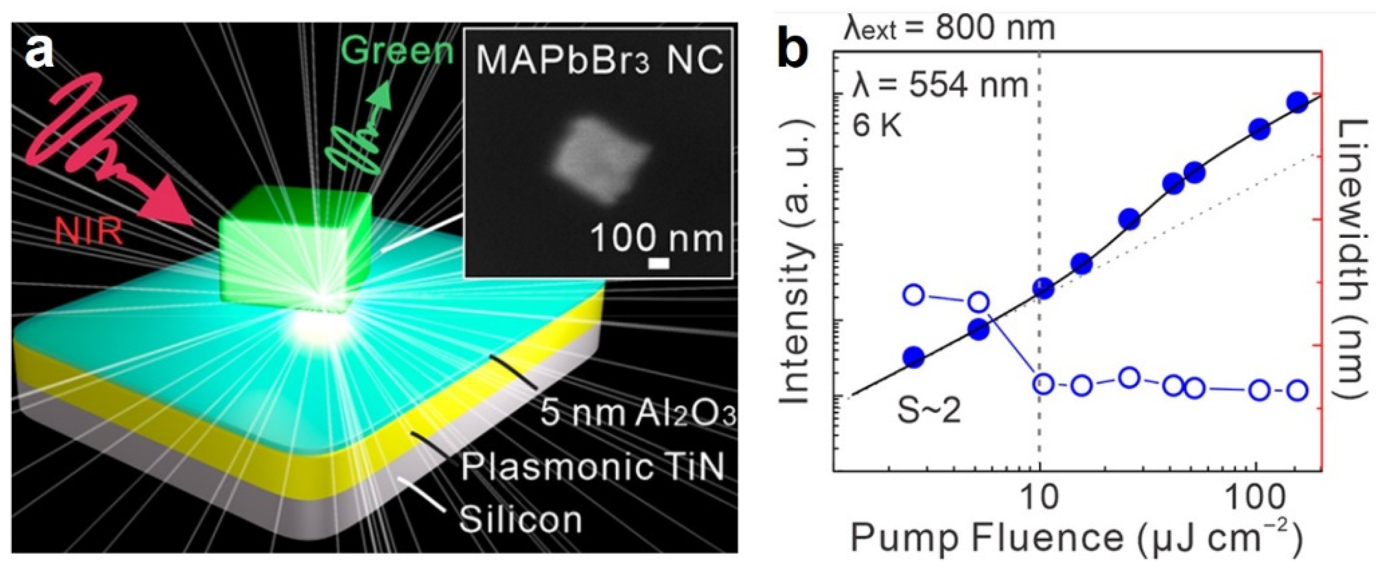
| MAPbBr3 | NCs | SP | 554 nm | 800 nm, 100 fs | 10 µJ/cm2 | 3 | 2021 [87] |
| CsPbBr3 | NCs | SP | 532 nm | 400 nm, 250 fs | 46.8 µJ/cm2 | 20.9 | 2022 [88] |
Publisher’s Note: MDPI stays neutral with regard to jurisdictional claims in published maps and institutional affiliations. |
© 2022 by the authors. Licensee MDPI, Basel, Switzerland. This article is an open access article distributed under the terms and conditions of the Creative Commons Attribution (CC BY) license (https://creativecommons.org/licenses/by/4.0/).
Share and Cite
Zhang, N.; Na, Q.; Xie, Q.; Jia, S. Development of Solution-Processed Perovskite Semiconductors Lasers. Crystals 2022, 12, 1274. https://doi.org/10.3390/cryst12091274
Zhang N, Na Q, Xie Q, Jia S. Development of Solution-Processed Perovskite Semiconductors Lasers. Crystals. 2022; 12(9):1274. https://doi.org/10.3390/cryst12091274
Chicago/Turabian StyleZhang, Nan, Quanxin Na, Qijie Xie, and Siqi Jia. 2022. "Development of Solution-Processed Perovskite Semiconductors Lasers" Crystals 12, no. 9: 1274. https://doi.org/10.3390/cryst12091274