

Isotropic TFT Characteristics in the {100}-Oriented Grain-Boundary-Free Laser-Crystallized Si Thin Films


Abstract
:1. Introduction
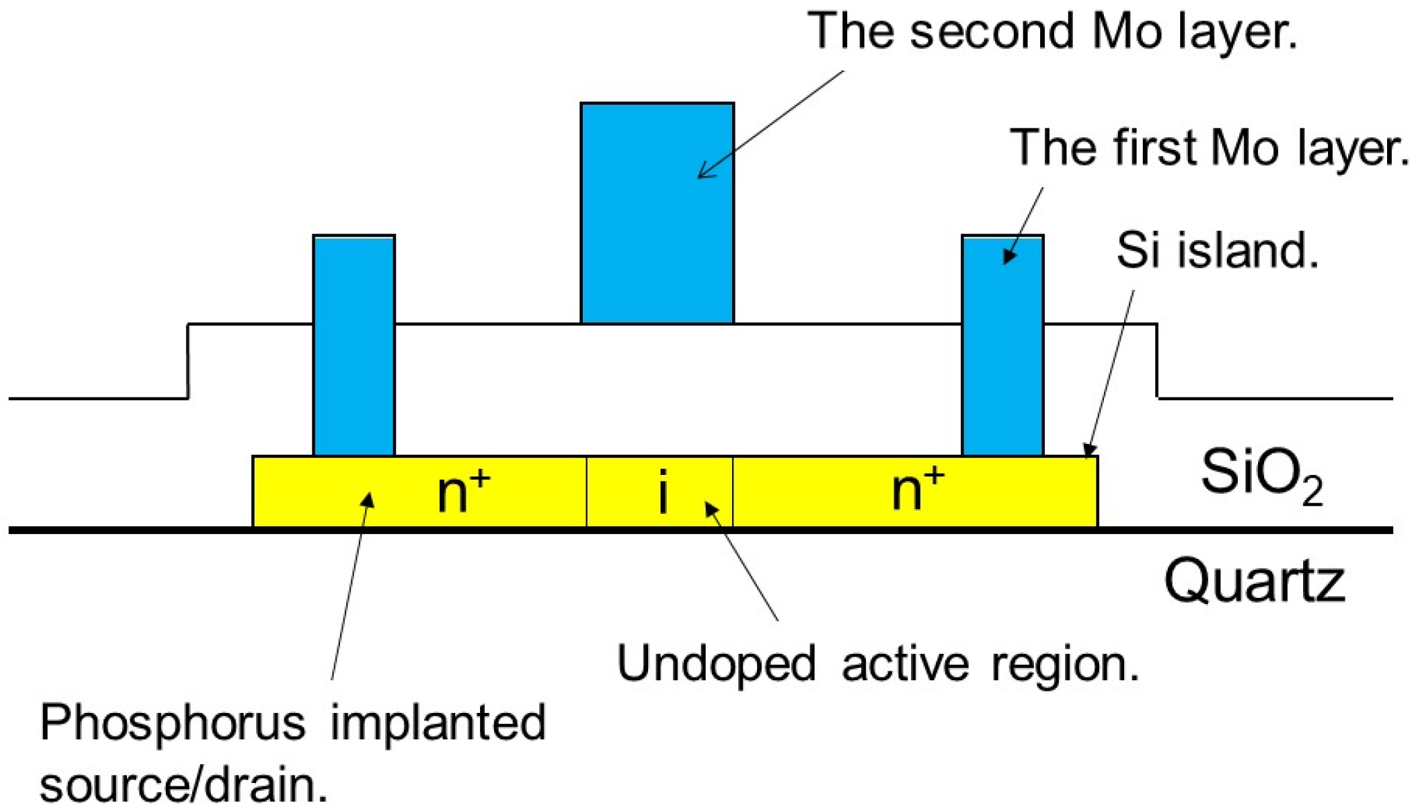
2. Experimental
3. Results
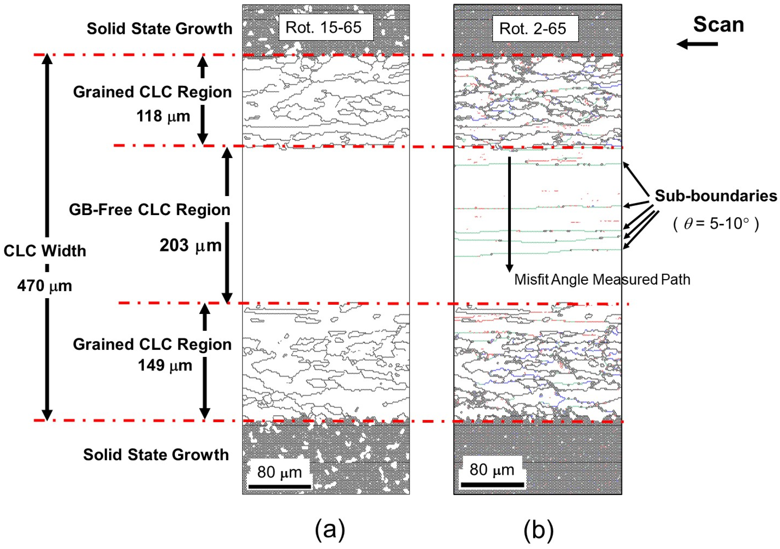
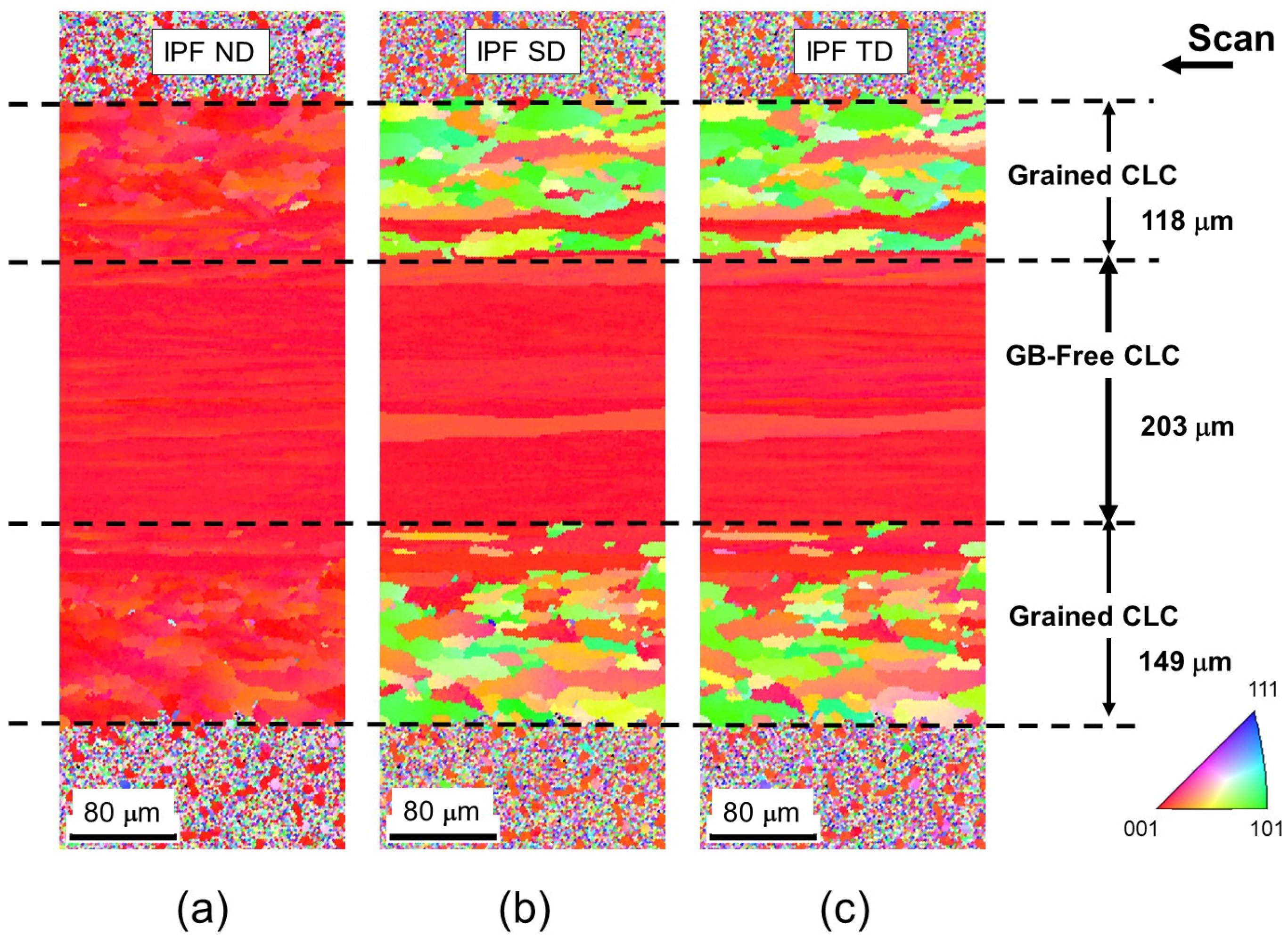
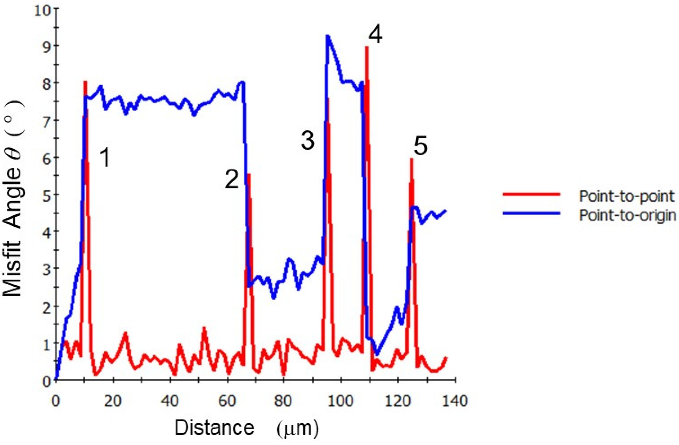
3.1. The Sub-Grains (Sub-G) and Sub-Boundaries (Sub-B) in the GB-Free Area
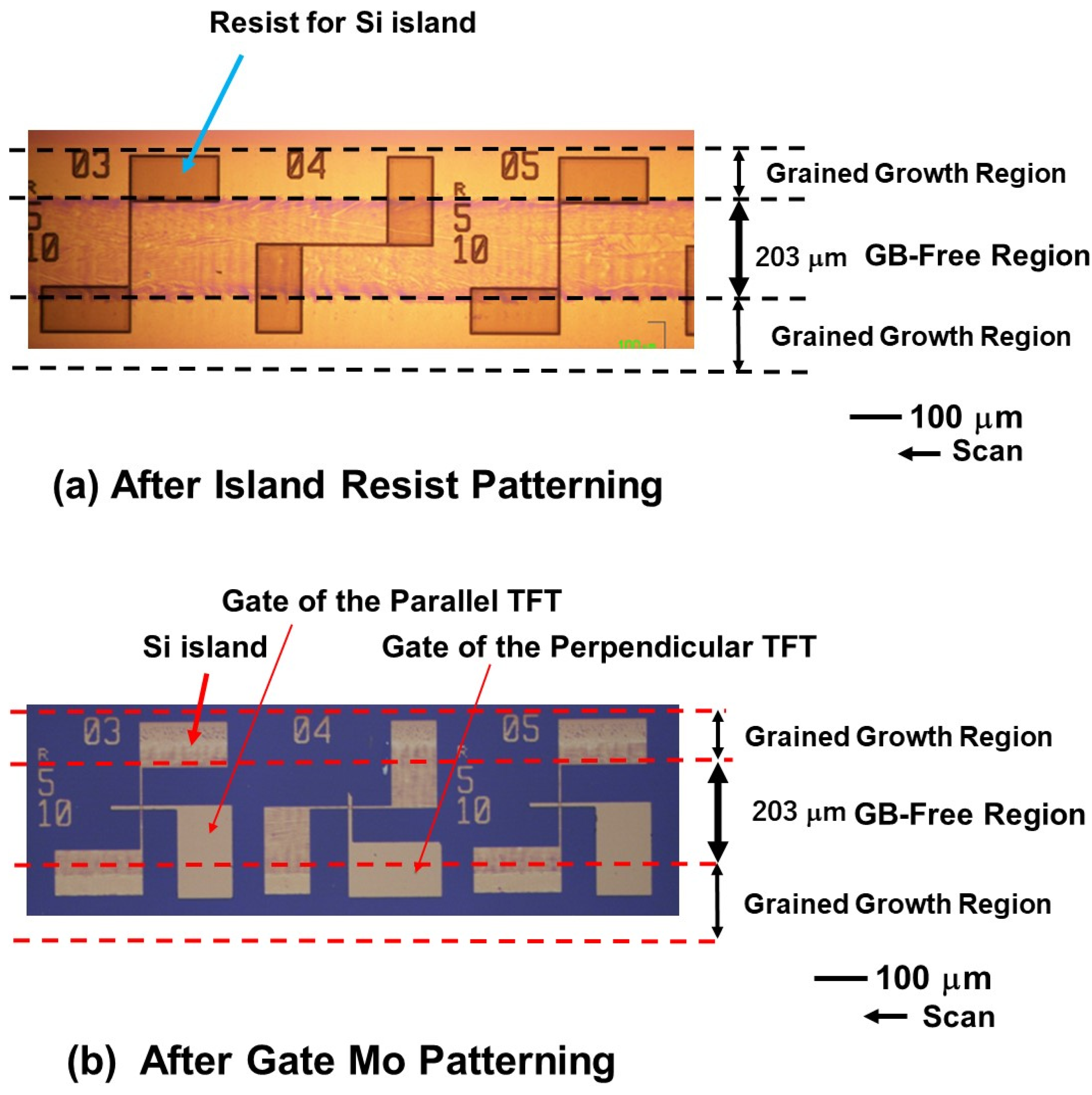
3.2. TFT Alignment in the Laser Scanned Stripe and Contact Resistance
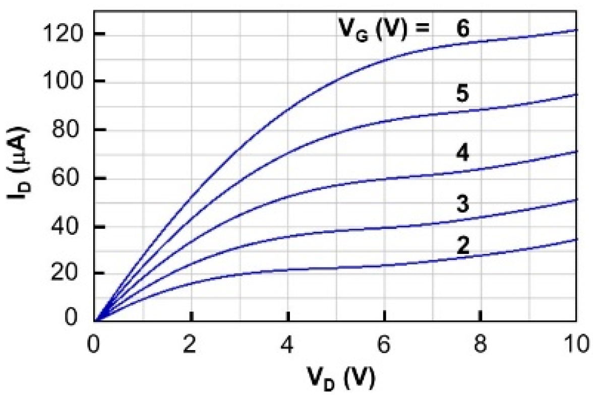
3.3. TFT Characteristics in the GB-Free CLC Region
3.4. TFT Characteristic in the Grained CLC Region
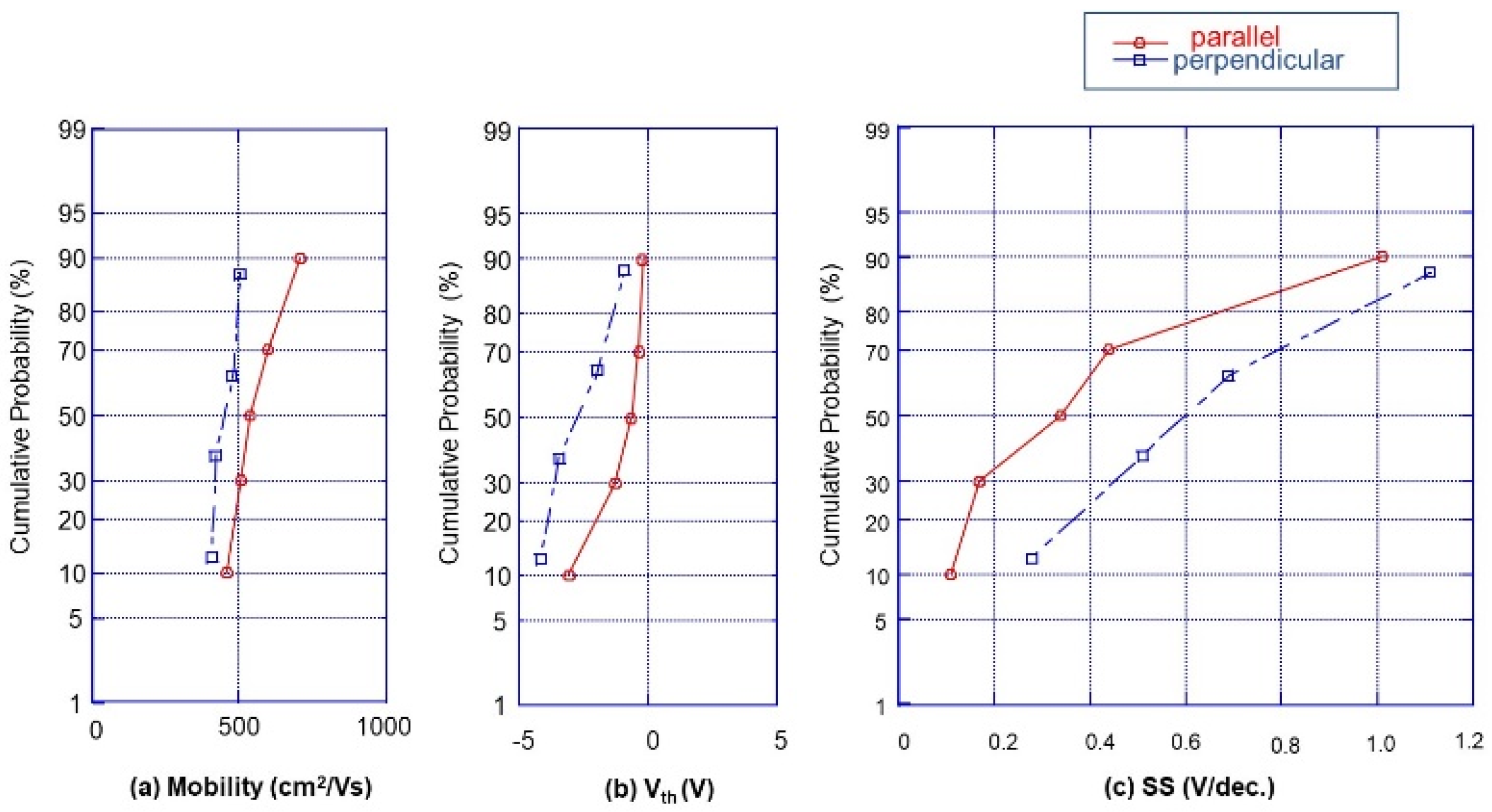
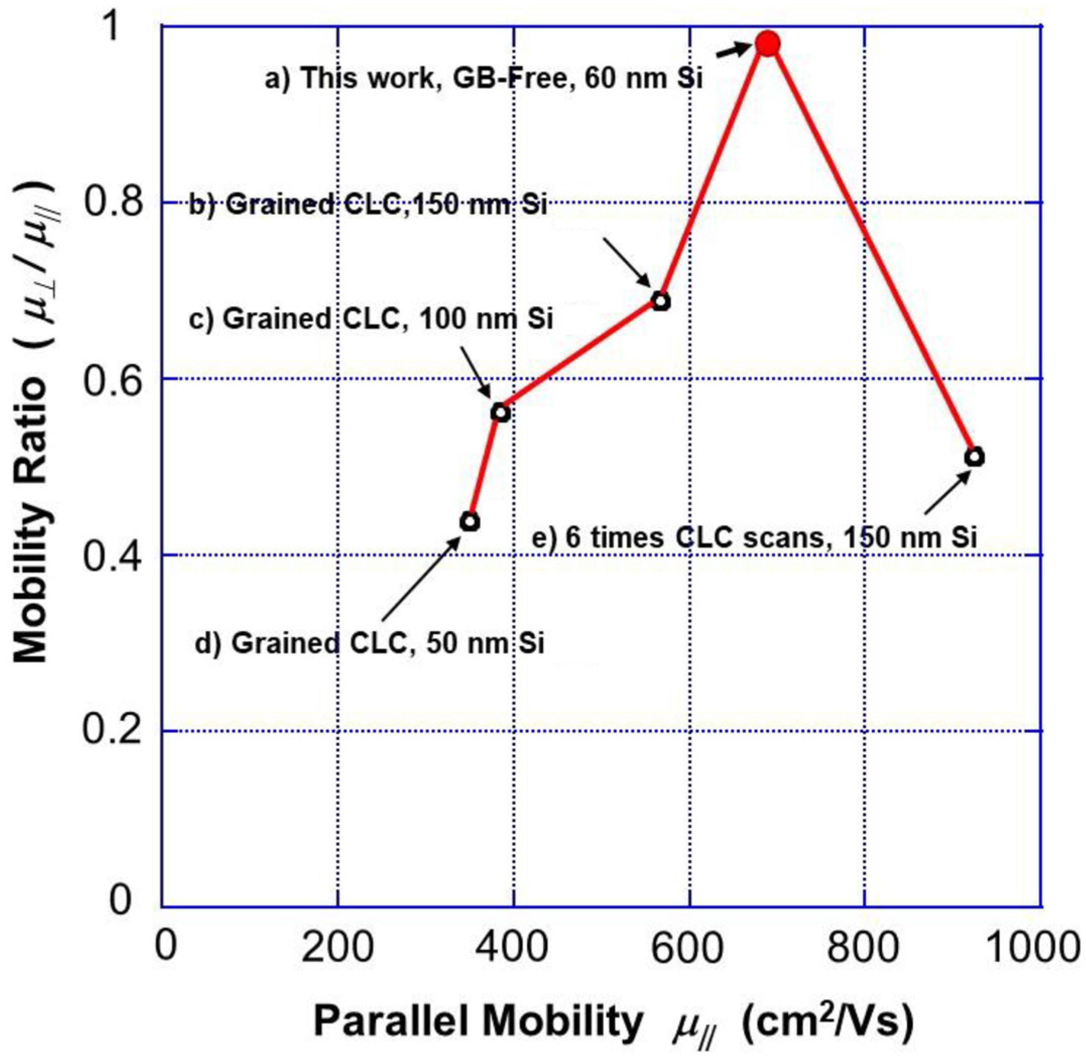
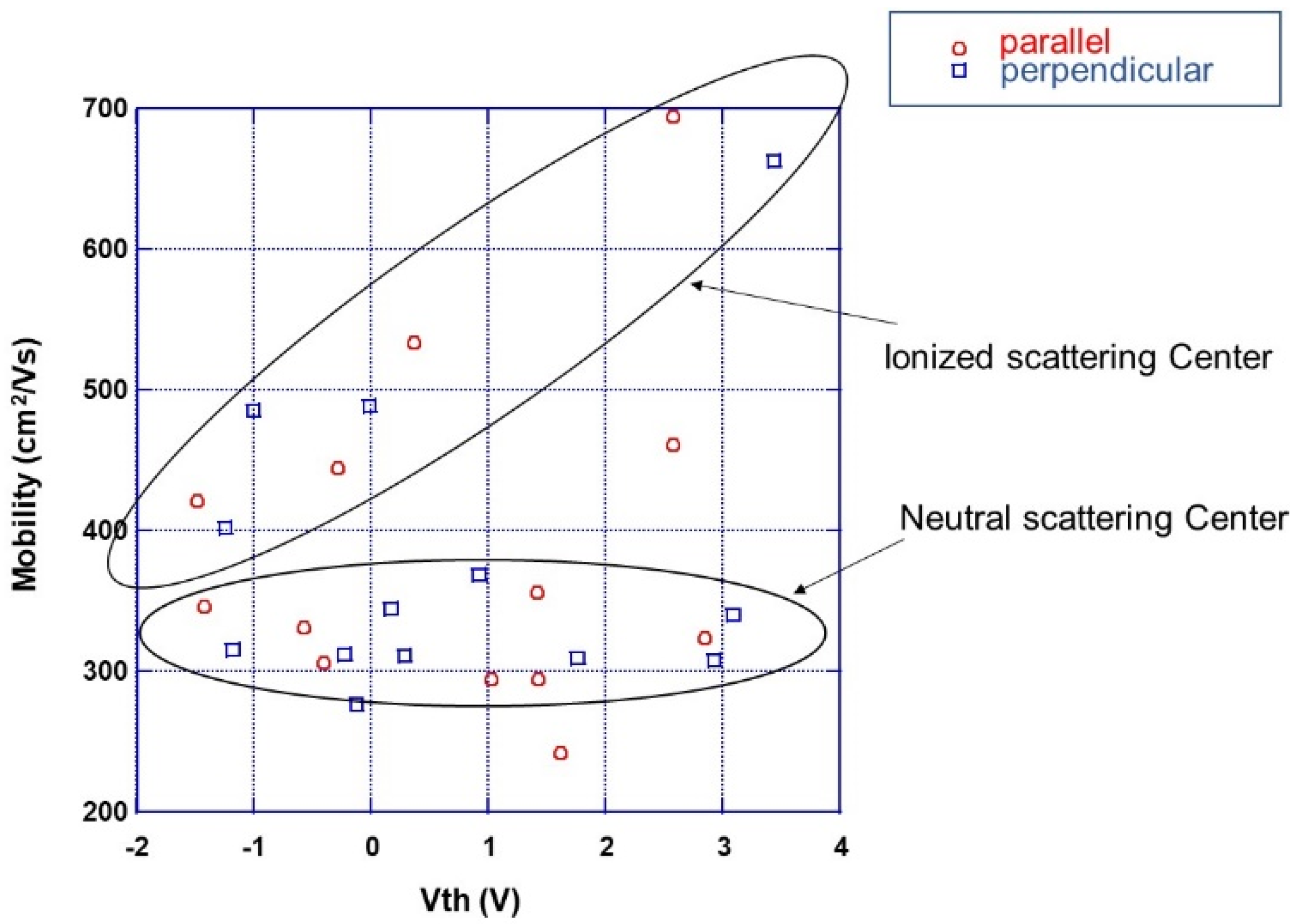
3.5. Comparison of Mobility Ratio Fabricated in the Present GB-Free CLC Film with Those in Other CLC Films
4. Theoretical Considerations and Its Comparison with Experimental Results
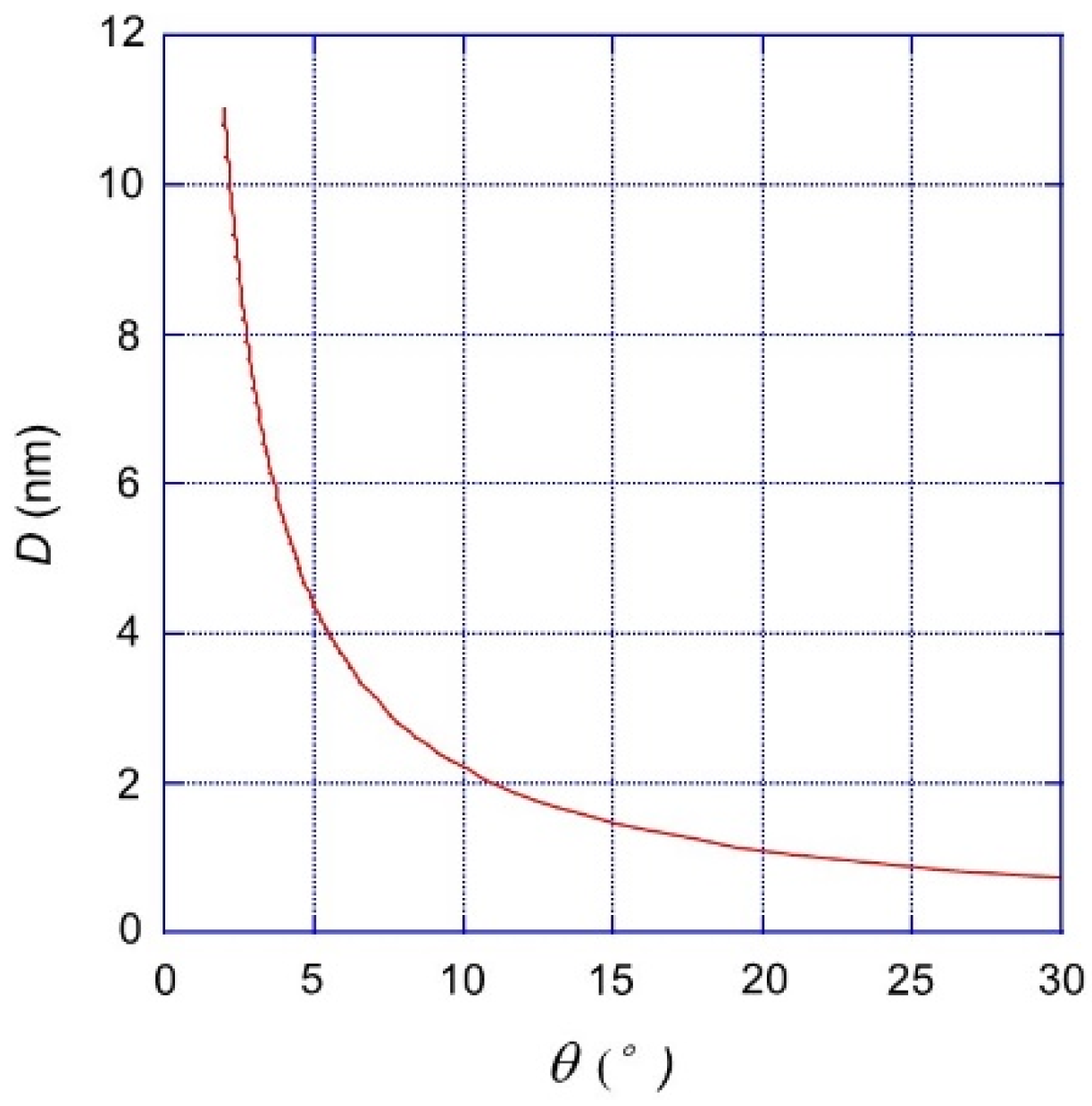
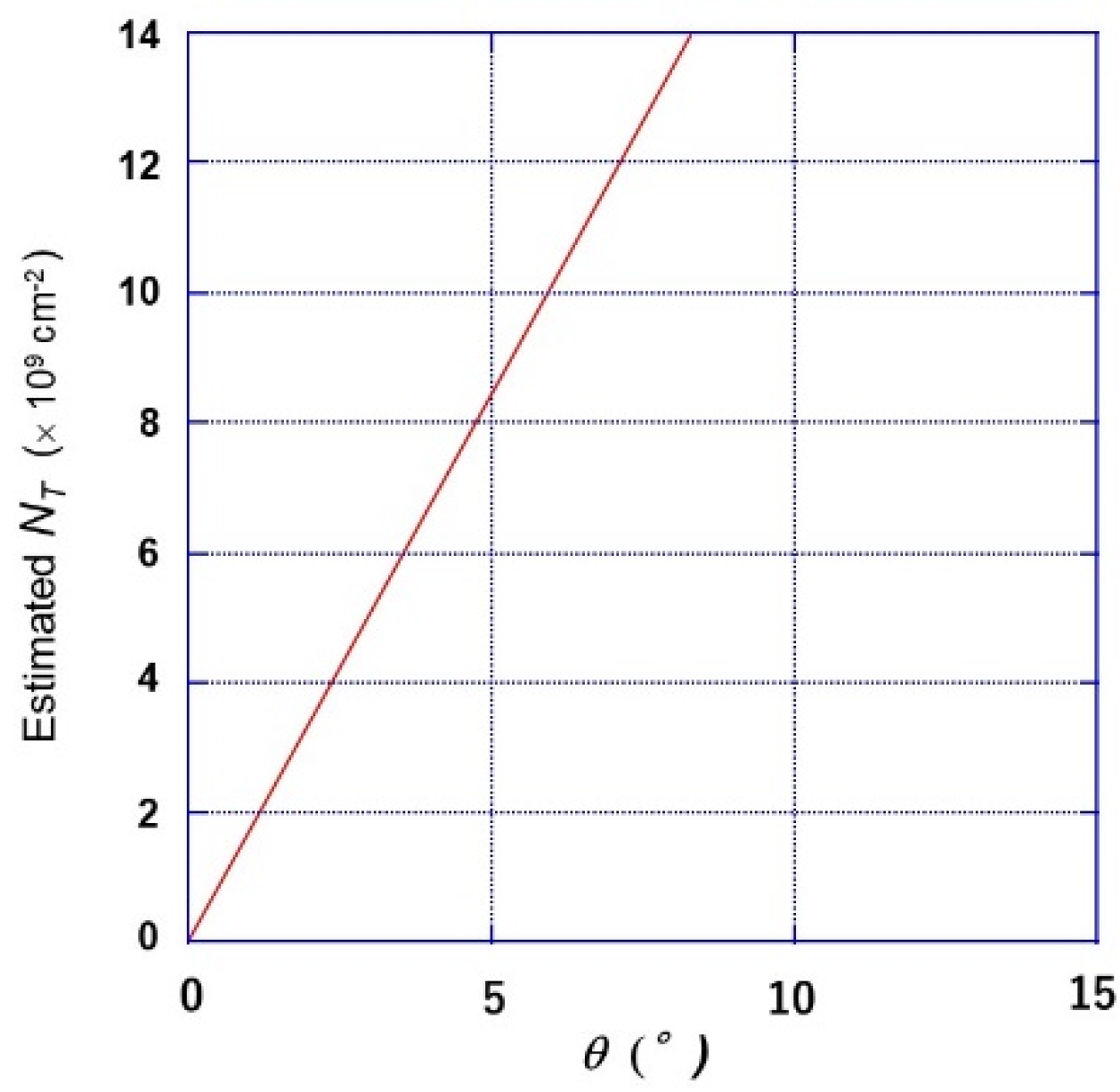
4.1. Trap-State Density at the Sub-Boundaries
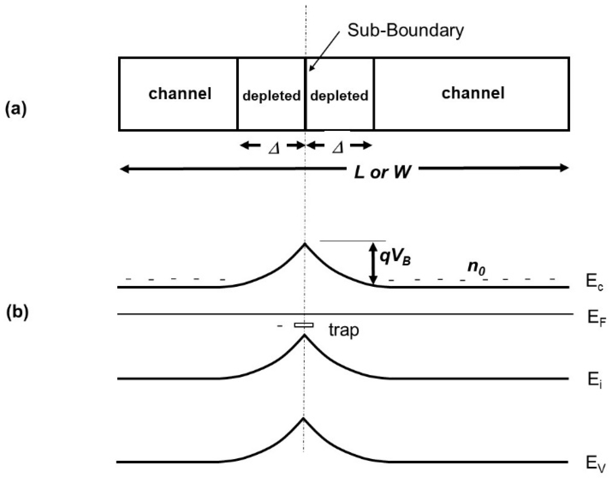
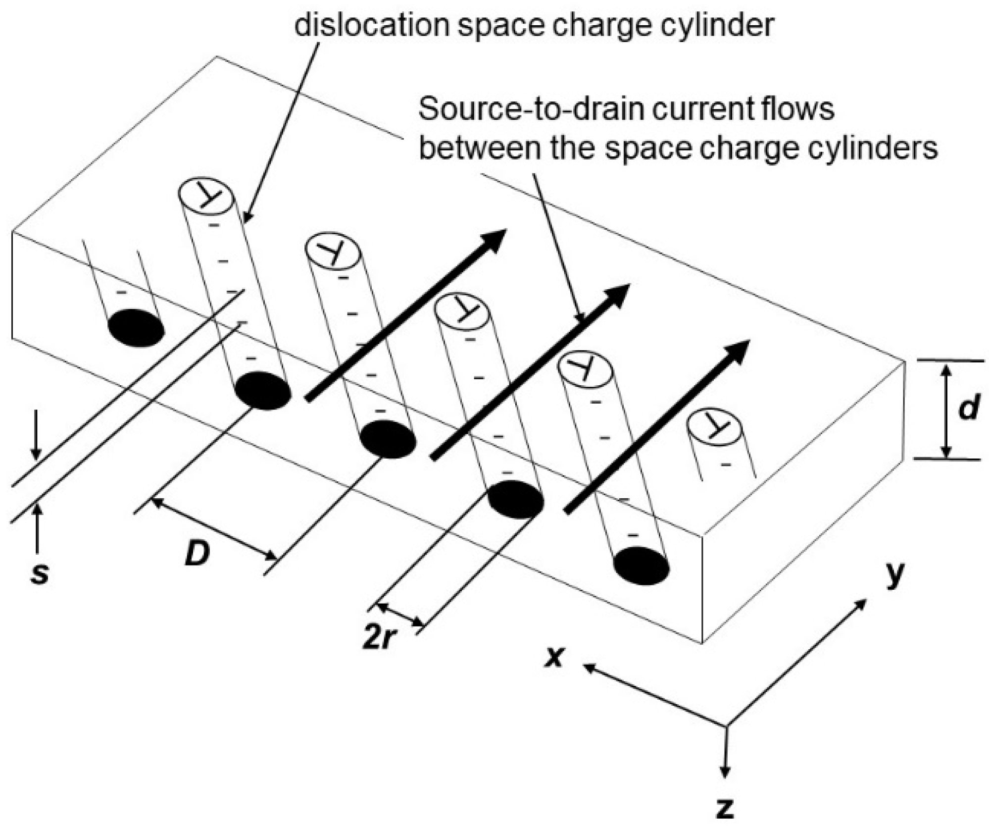
4.2. Space Charge Model at the Sub-Boundaries in the Non-Doped Substrate
4.3. Carrier Conduction in the Parallel TFTs
4.4. Carrier Conduction in the Perpendicular TFTs
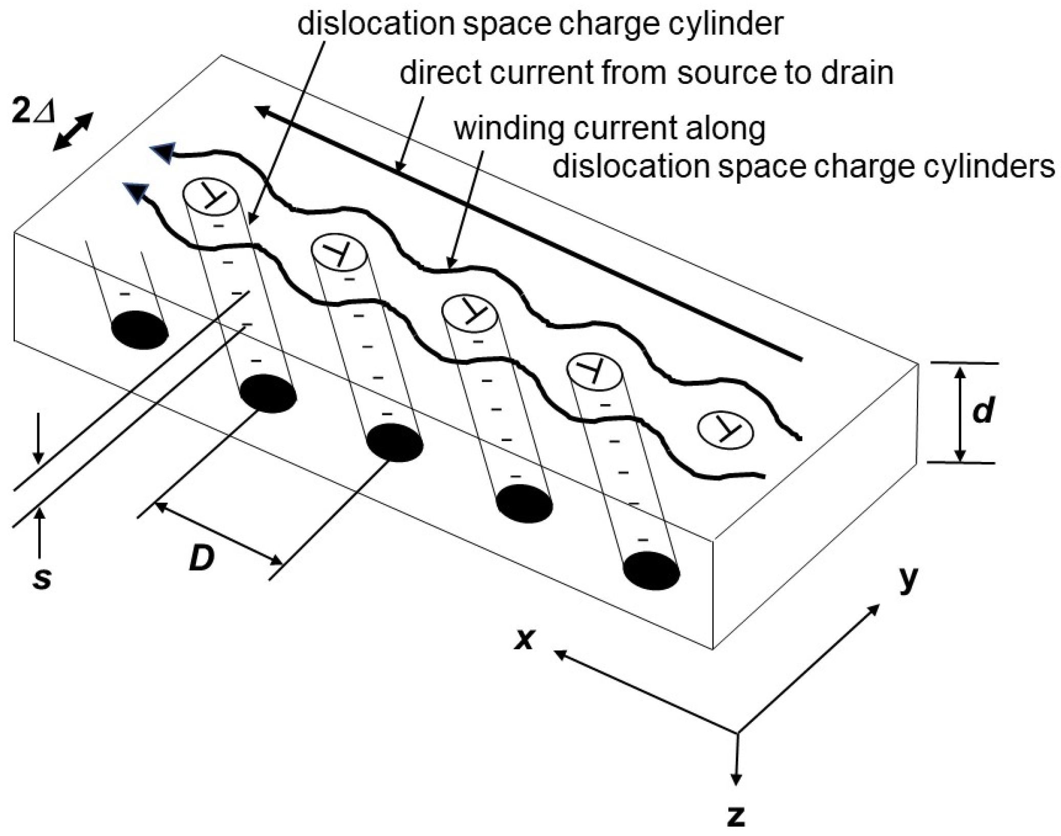
4.5. A New Model of the Perpendicular Carrier Conduction at the Sub-B
4.6. Origin of the Variations in Electrical Characteristics
5. Conclusions
Author Contributions
Funding
Data Availability Statement
Conflicts of Interest
References
- Cunningham, K.L. A process for using oxide TFTs over LTPS TFTs for OLED-TV manufacturing. Inf. Disp. 2015, 31, 28–32. [Google Scholar] [CrossRef]
- Avila-Avendano, C.; Solís-Cisneros, H.L.; Conde, J.; Sevilla-Camacho, P.A.; Quevedo-L, M.A. Modeling and SPICE simulation of the CdS/CDTe neutron detectors integrated with Si-Poly TFTs Amplifier. IEEE Trans. Nucl. Sci. 2022, 69, 1310–1315. [Google Scholar] [CrossRef]
- Bahubalindruni, P.G.; Martins, J.; Santa, A.; Tavares, V.; Martins, R.; Fortunato, E.; Barquinha, P. High-gain transimpedance amplifier for flexible radiation dosimetry using using InGaZnO TFTs. J. Electron Devices Soc. 2018, 6, 760–765. [Google Scholar] [CrossRef]
- Facchetti, A.; Hsiao, C.-C.; Huitema, E.; Inagaki, P. Enabling wearable and other novel applications through flexible TFTs. Inf. Disp. 2016, 32, 6–11. [Google Scholar] [CrossRef]
- Wager, J.F. Oxide TFTs: A progress report. Inf. Disp. 2016, 32, 16–21. [Google Scholar] [CrossRef]
- Brotherton, S.D.; McCulloch, D.; Clegg, J.; Gowers, J. Excimer-laser-annealed poly-Si thin-film transistors. IEEE Trans. Electron Devices 1993, 40, 407–413. [Google Scholar] [CrossRef]
- Mishima, Y.; Yoshino, K.; Takeuchi, F.; Ohgata, K.; Takei, M.; Sasaki, N. High-performance CMOS circuits fabricated by excimer-laser-annealed poly-Si TFTs on glass substrates. IEEE Elec. Dev. Lett. 2001, 22, 89–91. [Google Scholar] [CrossRef]
- Sasaki, N.; Hara, A.; Takeuchi, F.; Mishima, Y.; Kakehi, T.; Yoshino, K.; Takei, M. High throughput CW-laser lateral crystallization for low-temperature poly-Si TFTs and fabrication of 16 bit SRAMs and 270 MHz shift registers. SID Int. Symp. Dig. Tech. Pap. 2002, 33, 154–157. [Google Scholar] [CrossRef]
- Hara, A.; Takei, M.; Takeuchi, F.; Suga, K.; Yoshino, K.; Chida, M.; Kakehi, T.; Ebiko, Y.; Sano, Y.; Sasaki, N. High performance low temperature polycrystalline silicon thin film transistors on non-alkaline glass produced using diode pumped solid state continuous wave laser lateral crystallization. Jpn. J. Appl. Phys. 2004, 43, 1269–1276. [Google Scholar] [CrossRef]
- Park, M.; Vangelatos, Z.; Rho, Y.; Park, H.K.; Jang, J.; Grigoropoulos, C. Comprehensive analysis of blue diode laser-annealing of amorphous silicon films. Thin Solid Films 2020, 696, 137779. [Google Scholar] [CrossRef]
- Sasaki, N.; Arif, M.; Uraoka, Y.; Gotoh, J.; Sugimoto, S. Unseeded crystal growth of (100)-oriented grain-boundary-free Si thin-film by a single scan of the CW-laser lateral crystallization of a-Si on Insulator. Crystals 2020, 10, 405. [Google Scholar] [CrossRef]
- Nguyen, T.T.; Kuroki, S.-I. Dependence of thin film transistor characteristics on low-angle grain boundaries of (100)-oriented polycrystalline silicon thin films. Jpn. J. Appl. Phys. 2019, 58, SBBJ08. [Google Scholar] [CrossRef]
- Yeh, W.; Shirakawa, T.; Pham, A.H.; Morito, S. Twin formation in micro-chevron laser beam scanning induced one directional crystal growth in Si film on SiO2. Jpn. J. Appl. Phys. 2020, 59, SGGJ05. [Google Scholar] [CrossRef]
- Yeh, W.; Hirasue, M.; Ohtoge, K.; Tsuchiya, T. High performance thin-film transistors fabricated on a single crystal Si strip by micro-chevron laser beam scanning method. Jpn. J. Appl. Phys. 2020, 59, 071008. [Google Scholar] [CrossRef]
- Andersen, P.M.; Hirth, J.P.; Lothe, J. Grain boundaries and interfaces. In Theory of Dislocations, 3rd ed.; Cambridge Univ. Press: Cambridge, UK, 2017; pp. 536–540. [Google Scholar]
- Brandon, D.G. The structure of high-angle grain boundaries. Acta Metall. 1966, 14, 1479–1484. [Google Scholar] [CrossRef]
- Sasaki, N.; Nieda, Y.; Hishitani, D.; Uraoka, Y. Power dependence of orientation in low-temperature poly-Si lateral grains crystallized by a continuous-wave laser scan. Thin Solid Films 2017, 631, 112–117. [Google Scholar] [CrossRef]
- Sasaki, N.; Arif, M.; Uraoka, Y. Folded pixel circuit design in grain-boundary free (100) oriented LTPS stripes fabricated by selective CW-laser lateral crystallization. SID Int. Symp. Dig. Tech. Pap. 2018, 49, 755–758. [Google Scholar] [CrossRef]
- Sasaki, N.; Arif, M.; Uraoka, Y. Transition mechanism of the thin Si-films obtained by the CW laser lateral crystallization from the grain-boundary free highly {100} oriented crystal to the twinned {211} crystal depending on the laser power. Jpn. J. Appl. Phys. 2019, 58, SBBJ02. [Google Scholar] [CrossRef]
- Sasaki, N.; Arif, M.; Uraoka, Y. Effect of surface tension on crystal growth of Si thin films by a continuous-wave laser lateral crystallization. Appl. Phys. Express 2019, 12, 055508. [Google Scholar] [CrossRef]
- Arif, M.; Sasaki, N.; Ishikawa, Y.; Uraoka, Y. Extension of the {100}-oriented grain-boundary free Si thin film grown by a continuous-wave laser lateral crystallization. Thin Solid Films 2020, 708, 138127. [Google Scholar] [CrossRef]
- Arif, M.; Sasaki, N.; Takayama, S.; Uraoka, Y. Extension of a 10 mm long {100}-oriented grain boundary free silicon domain crystallized by continuous wave green laser. In Proceedings of the 21st International Meeting on Information Display, Virtual, 25–27 August 2021. [Google Scholar]
- Sasaki, N.; Arif, M.; Uraoka, Y.; Gotoh, J.; Sugimoto, S. Crystal growth study of the grain-boundary free (100) textured Si thin films by using the CW-laser lateral crystallization. In Proceedings of the IEEE SOI-3D-Subthreshold Microelectronics Technology Unified (S3S) Conference, San Jose, CA, USA, 14–17 October 2019. [Google Scholar] [CrossRef]
- Sasaki, N.; Arif, M.; Uraoka, Y.; Gotoh, J.; Sugimoto, S. Continuous-wave laser lateral crystallization of a-Si thin films on polyimide using a heatsink layer embedded in the buffer SiO2. J. Electron. Mat. 2021, 50, 2974–2980. [Google Scholar] [CrossRef]
- Sasaki, N.; Arif, M.; Takayama, S.; Gotoh, J.; Sugimoto, S.; Uraoka, Y. Isotropic TFT mobility in the (100)-oriented grain-boundary-free huge Si thin film grown by the continuous-wave-laser lateral crystallization. In Proceedings of the 2021 International Conference on Solid State Devices and Materials, Virtual, 6–9 September 2021. [Google Scholar]
- Sodini, C.G.; Ekstedt, T.W.; Moll, J.L. Charge accumulation and mobility in thin dielectric MOS transistors. Solid-St. Electron. 1982, 25, 833. [Google Scholar] [CrossRef]
- Chen, K.; Wann, H.C.; Dunster, J.; Ko, P.K.; Hu, C.; Yoshida, M. MOSFET carrier mobility model based on gate oxide thickness, threshold and gate voltages. Solid-St. Electron. 1996, 39, 1515. [Google Scholar] [CrossRef]
- Yang, G.-Y.; Hur, S.-H. A physical-based analytical turn-on model of polysilicon thin-film transistors for circuit simulation. IEEE Trans. Electron Devices 1999, 46, 165. [Google Scholar] [CrossRef]
- Sasaki, N. Change of Si-SiO2 Interface Charge by BT Treatment. Jpn. J. Appl. Phys. 1973, 12, 1458–1459. [Google Scholar] [CrossRef]
- Sze, S.M. Crystal Orientation Effect. In Physics of Semiconductor Devices; Wiley: New York, NY, USA, 1969; pp. 471–473. [Google Scholar]
- Andersen, P.M.; Hirth, J.P.; Lothe, J. Core energy. In Theory of Dislocations, 3rd ed.; Cambridge Univ. Press: Cambridge, UK, 2017; pp. 203–207. [Google Scholar]
- Mataré, H.F. Basic electrical properties of dislocations in semiconductors. In Defect Electronics in Semiconductors; Wiley: New York, NY, USA, 1971; pp. 145–172. [Google Scholar]
- Seto, J.Y. The Electrical Properties of Polycrystalline Silicon Films. J. Appl. Phys. 1975, 46, 5247–5254. [Google Scholar] [CrossRef]
- Baccarani, G.; Riccò, B.; Spadini, G. Transport properties of polycrystalline silicon films. J. Appl. Phys. 1978, 49, 5565–5570. [Google Scholar] [CrossRef]
- Lu, N.C.-C.; Gerzberg, L.; Lu, C.-Y.; Meindl, J.D. Modeling and Optimization of Monolithic Polycrystalline Silicon Resistors. IEEE Trans. Electron Devices, 1981; ED-28, 818–830. [Google Scholar] [CrossRef]
- Levinson, J.; Shepherd, F.R.; Scanlon, P.J.; Westwood, W.D.; Este, G.; Rider, M. Conductivity behavior in Polycrystalline Semiconductor Thin Film Transistors. J. Appl. Phys. 1982, 53, 1193–1202. [Google Scholar] [CrossRef]
- Fossum, J.G.; Oritz-Conde, A. Effects of grain boundaries on the channel conductance of SOI MOSFET’s. IEEE Trans. Electron Devices 1983, ED-30, 933–940. [Google Scholar] [CrossRef]
- Martinez, J.; Criado, A.; Piqueras, J. Grain boundary potential determination in polycrystalline silicon by the scanning light spot technique. J. Appl. Phys. 1981, 52, 1301. [Google Scholar] [CrossRef]
- Proano, R.E.; Ast, D. Effects of the presence/absence of HCl during gate oxidation on the electrical and structural properties of polycrystalline silicon thin-film transistors. J. Appl. Phys. 1989, 66, 2189. [Google Scholar] [CrossRef]
- Walker, P.M.; Mizuta, H.; Uno, S.; Furuta, Y.; Hasko, D.G. Improved off-current and subthreshold slope in aggressively scaled poly-Si TFTs with a single grain boundary in the channel. IEEE Trans. Electron Devices 2004, 51, 212. [Google Scholar] [CrossRef] [Green Version]
- Takagi, S.; Toriumi, A.; Iwase, M.; Tango, H. On the universality of inversion layer mobility in Si MOSFET’s: Part I-effects of substrate impurity concentration. IEEE Trans. Electron. Devices 1994, 41, 2357–2362. [Google Scholar] [CrossRef]


| Data Source From | NT (cm−2) | Grain Size (nm) |
|---|---|---|
| Seto, 1975 [33] | 3.41 × 10¹² | 23 |
| Baccarani et al., 1978 [34] | 3.80 × 10¹² | 30 |
| Lu et al., 1981 [35] | 2.10 × 10¹² | 122 |
| Martinez et al., 1981 [38] | 1.2 × 10¹³ | 1 × 10⁵ |
| Levinson et al., 1982 [36] | 3.9 × 10¹¹ | 40 |
| Fossum et al., 1983 [37] | 1.00 × 10¹² | 1 × 10³ |
| Proano et al., 1989 [39] | 1.1 ~ 2.0 × 10¹² | 100 |
| Yang et al.,1999 [28] | 2.5 × 10¹² | 200 |
| Walker et al.,2004 [40] | 1.0 × 10¹³ | ------- |
| This Work | 0.8 ~ 1.6 × 10¹⁰ (Sub-B) | 2.03 × 10⁵ (Perpendicular Grain Width ) 3.38 × 10⁴ (Perpendicular Sub-G Width ) |
Disclaimer/Publisher’s Note: The statements, opinions and data contained in all publications are solely those of the individual author(s) and contributor(s) and not of MDPI and/or the editor(s). MDPI and/or the editor(s) disclaim responsibility for any injury to people or property resulting from any ideas, methods, instructions or products referred to in the content. |
© 2023 by the authors. Licensee MDPI, Basel, Switzerland. This article is an open access article distributed under the terms and conditions of the Creative Commons Attribution (CC BY) license (https://creativecommons.org/licenses/by/4.0/).
Share and Cite
Sasaki, N.; Takayama, S.; Sasai, R.; Uraoka, Y. Isotropic TFT Characteristics in the {100}-Oriented Grain-Boundary-Free Laser-Crystallized Si Thin Films. Crystals 2023, 13, 130. https://doi.org/10.3390/cryst13010130
Sasaki N, Takayama S, Sasai R, Uraoka Y. Isotropic TFT Characteristics in the {100}-Oriented Grain-Boundary-Free Laser-Crystallized Si Thin Films. Crystals. 2023; 13(1):130. https://doi.org/10.3390/cryst13010130
Chicago/Turabian StyleSasaki, Nobuo, Satoshi Takayama, Rikuto Sasai, and Yukiharu Uraoka. 2023. "Isotropic TFT Characteristics in the {100}-Oriented Grain-Boundary-Free Laser-Crystallized Si Thin Films" Crystals 13, no. 1: 130. https://doi.org/10.3390/cryst13010130
APA StyleSasaki, N., Takayama, S., Sasai, R., & Uraoka, Y. (2023). Isotropic TFT Characteristics in the {100}-Oriented Grain-Boundary-Free Laser-Crystallized Si Thin Films. Crystals, 13(1), 130. https://doi.org/10.3390/cryst13010130