1. Introduction
Silicon-based nanoelectronics have now reached their physical limits. The ongoing trend towards the further optimization of related devices currently emphasizes the importance of both semiconductor active channels with mobile two-dimensional electron gas (2D EG) and dielectric gate layers with a nano-scale-equivalent oxide thickness [
1,
2]. In this regard, semiconductors of the III–V group [
3], metal dichalcogenides and few-layer graphenes [
4] are currently the most promising candidate materials due to their high switching speed and low power consumption, which are important requirements for nanodevices. In turn, high-κ dielectric gate oxides, such as Al
2O
3 [
5] and HfO
2 [
6], as well as HfO-AlO [
7,
8], ZrO-AlO [
8], HfO-LaO [
9] and HfO-chalcogenide [
10] nanolaminate alloy forms, are currently of key interest. The aforementioned active channel materials possess a narrow energy band gap, resulting in the easy generation of defect states, for example, in the multi-layer quantum structure [
7]. Certainly, such states can directly affect transport and optical properties, and clarifying the specific roles of defect states, impurity states in particular, in the noted system is fundamental [
11].
In the present work, the task is to investigate the effect of screening mechanisms on impurity states in a multi-layer quantum structure by studying the impurity optical characteristics, namely, both the calculable and measurable quantities of the impurity binding energy. As for the study of transport characteristics (the scattering rate and mobility) under these conditions, we strictly intend to address this in our forthcoming article.
Generally, an active 2D EG channel in a multi-layer device structure operates under a static polarization field caused by a dielectric mismatch between the componential semiconductor and dielectric layers [
12,
13,
14,
15,
16]. However, for the nano-scale thickness values of the dielectric layers (both passivation and oxide), an additional part of the polarization field might be induced by the existing metal gate [
17,
18]. So, these fields’ resultant substrate screening (SS) mechanism, which is initiated by the image charges located in both the dielectric and metal gate layers, can, together with the 2D EG electronic screening (ES) mechanism [
14,
15], significantly re-normalize the Coulomb interaction of the background impurity centers that occur (intentionally or not) in the active semiconductor channel of the multi-layer structure. As a result, unique circumstances are created in these nanostructures that allow for the manipulation of the physical characteristics of the comprehensively screened impurities via an inter-correlation of important parameters, such as (a) the in-plane density of the 2D EG, (b) the dielectric constants of the semiconductor and oxide layer media and the (c) nano-scale thickness of the oxide layers.
In this regard, since the Coulomb interaction is a key factor for any reliable predictions of dielectrically inhomogeneous system properties to be made [
19,
20], clarifying the role of the impurity states in the semiconductor inversion layers of a multi-layer structure simultaneously influenced by ES and SS mechanisms is currently fundamental, and it is only just starting to be unraveled [
7,
17,
18,
21].
Theoretical studies of the screened Coulomb interaction in the noted system emerged in articles published after [
14], wherein the Coulomb screening potential long-range spatial behavior of a point charge at the 2D limit is revealed in contrast to the short-range nature of that in a 3D case. An analogous result of QW structures was simultaneously established in [
21]. However, in [
14] and the work that followed regarding the screened impurity properties of 2D systems (see [
15,
19,
21,
22,
23] and Refs.13–29 in [
21]]), metal-gate-induced polarization issues were mostly overlooked because general bulk dielectric environment models were developed. The multi-layer structure metal-gate-induced polarization screening effect caused by a thin dielectric layer was taken into account for the first time by Chaplik [
12]. Further, the features of such a specific type of screening effect were discussed in relation to problems mainly associated with the 2D EG plasmon and surface excitation [
12,
13,
17,
24,
25], carrier momentum relaxation time and mobility [
17] and the screened Coulomb interaction intensity [
18] phenomena.
As for the problems related to the screened impurity properties of inversion layers, a complete analytical study has not been carried out to date. In the article presented here, such a problem is developed analytically based on first principles. A wide variety of new analytical features of background impurity screening potential, which are lacking elsewhere, are established. Within the framework of the obtained results, the problem of comprehensively screened background impurity properties (bound state effective radius, effective screening length and bound state binding energy) of multi-layer quantum structures is considered for the first time. A numerical exploration based on realistic heterointerfaces appropriate for the developed theoretical model is also presented.
2. Screened Coulomb Interaction Potential
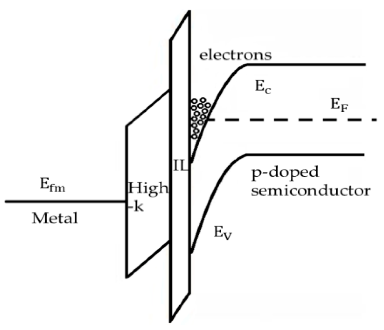
Let us have a multi-layer model structure (
Figure 1) where the region
z ≤ −(L + D) is occupied by the gate metal, the region
−(
L +
D) <
z ≤ −
L is filled by the dielectric oxide layer of thickness
D and dielectric constant
, the region
−L <
z ≤ 0 is filled by the dielectric passivation inter-layer (IL) of thickness
L and dielectric constant
, and finally the region 0 <
z ≤
∞ is occupied by the semiconductor with the dielectric constant
and the dotted line here represents the inversion channel boundary. Here, the z axis is perpendicular to the gate layer interfaces. In order to offer more visibility in
Figure 2, the band vending diagram of the discussed structure is also given.
In the model under discussion, the
n-type 2D EG channel with average surface density nS produces the free carrier screening of the impurity charge center sited at the point
ρ = 0,
z =
z0 > 0 near the semiconductor/oxide heterojunction. The screened Coulomb interaction potential
φ(
ρ,
z) of the impurity center is related to Poisson’s equation as
where
δ is the Dirac delta function,
=
(
,
z), and
ρ is the 2D plane coordinate.
In Equation (1),
ρi is the induced charge density, which, according to the Tomas–Fermi method, has the form [
14]:
where
µ0 ≫
kBT is the chemical potential in the absence of the Coulomb perturbing field,
kBT is the energy scale factor,
is the normalized charge distribution,
ψ(
z) is the self-consistent effective mass equation normalized solution of the electrons transverse motion, and
is averaged over the z coordinates by
ψ(
z) screened potential as
which gives no change in the normalized eigenfunction
ψ(
z) of the electrons’ effective mass equation but gives a difference in its eigenvalue. The ratio (
) in Equation (2) on the condition of the size quantum limit, i.e., when the one-particle ground quantum sublevel is occupied only and the electrons are essentially confined to move in an active channel plane, is determined from the Debye model as
where
me is the electron effective mass.
Poisson’s Equation (1) with Equations (2) and (4) then obtains the form:
and
where
is the screening parameter of the 2D EG as:
In particular, Equation (6) for the degenerate and non-degenerate 2D EG statistics correspondingly takes the forms:
and
To solve Equation (1), we employ the cylindrical coordinate system
ρ,
φ,
z, and, thus, express the interaction potential in Fourier components
φ(
k,
z) with respect to the coordinate
ρ as
where
is the electron 2D plane wave vector and
J0 is the zero-th order Bessel function.
Poisson’s Equation (1) with Equation (8) for the discussed model structure now obtains the form:
and
where
The system of Equation (9) would be solved by applying the appropriate electrostatic boundary conditions:
The appropriate general solutions of the corresponding inhomogeneous and homogeneous Equations (9a) and (9b) are
and
where
,
and
(
I = 1, 2, 3) are the coefficients to be determined by Equation (10). In Equation (11b), the screening influence by the gate metal on the induced potential is taken into account by imposing the condition
φk(
z) = 0 while following Equation (11a). Among the coefficients
Ci, only
C1 corresponds to the channel region and has to be calculated. Applying the boundary conditions after Equation (10) at the
i-th interface, we obtain
C1 as
where
and
are determined by
As a result, the general solution of Equation (9a) is
where
and
Equations (14) and (15) present the screened Coulomb interaction potential Fourier component related to the active channel region for the discussed multi-layer structure.
Here, we take an active channel carrier’s strong quantum confinement (QC) regime under the conditions
≫
d,
≫
d, where
and
are the effective Bohr and Debye radii in the bulk semiconductor, respectively, and
d is the active layer effective thickness. The parameter
d/
a0 determines a criterion of two-dimensionality of the problem, and for that, as shown in [
26], an active channel plasma should be dense and, therefore, weakly nonideal. To the latter in size, quantum limit corresponds to the condition
≫ 1, meaning that the number of surface electrons on the area of the Bohr orbit should be large enough.
With these conditions in Equations (14) and (15), an important role will be played by 2D distances of
ρ ≫
d, since in the 2D wave vector k interval exists, hence
k d ≪ 1. As follows, Equations (14) and (15) should be averaged under the conditions
q z ≪ 1 and
q z0 ≪ 1, which permits in the leading order of the parameter
d/
a0 to obtain a solution of Equation (9a) for any arbitrary normalized charge distribution function
g(
z). Such a calculation gives the result as
which, jointly with Equation (13), generalizes for the first time all similar analytical expressions received before for the individual screening cases in the framework of the 2D screening theory related to the multi-layer structures.
Since the realistic multi-layer engaged nanodevices possess both sufficiently thin passivation and oxide gate layers, Equation (13) should be modified following the long wave-related conditions
qL ≪ 1 and
qD < 1. The result in Equation (13) should be modified following the long wave-related conditions
qL ≪ 1 and
qD < 1. The result with the accuracy of the small term (
q L) (
q D) transforms Equation (16) to the form:
where
is the effective screening parameter formed jointly by the ES and SS mechanisms.
If substitution of Equation (17) into Equation (8) is applied for the demanded 2D distances of ρ ≫ d, then the real-space interaction energy
(
ρ) = −
e (
ρ) of the
e and −
e impurity point charges takes the form:
where
H(
x) and
N(
x) are Struve and Neumann functions.
The screened Coulomb interaction energy
VS(
ρ) in the discussed case holds the same
k and
ρ dependences as the corresponding value in the multi-layer quantum structure with the bulk dielectric layer [
14,
15], but is enhanced twice (due to the factor
εS/2) in relation to the dielectrically homogeneous (
) structure. A similar result is also obtained in the screening problems with the nano-scale thickness dielectric layer for any proportion of
and
in the multi-layer quantum structure [
18] and with the bulk low-κ-type dielectric layer in the three-layer quantum systems [
22,
26,
27].
In turn, following Equations (18) and (19), the interaction energy VS(ρ) is characterized by the more general (compared to previous cases) effective screening parameter , which depends simultaneously on the key physical parameters of 2D EG and dielectric layers (, , , L, D).
In the accepted accuracy by the small-term (
q L) (
D) in Equation (18), the passivation and oxide dielectric layer parameters in
enter symmetrically and the replacement of indices
will have no physical consequences. In this regard, it should be noted that in the real multi-layer quantum structure [
2,
4,
5,
6,
7,
8,
9,
10], the thickness of the passivation layer (~0.05–0.15 nm) is usually small compared to the thickness of the oxide layer (~2–10 nm), and we utilize such a realistic structural design here.
By itself, Equation (18) generalizes the previously derived screening parameter expressions concerning the ES (first term in Equation (18)), as well as the SS mechanisms (second term in Equation (18)), respectively. It is distinctive that in
, the contributions being produced by the above-mentioned screening mechanisms are characterized by separate terms, i.e., additively. So, the oxide layer thickness nano-scale values lead to the corresponding separate terms in the effective screening parameter
as
and
The cross-correlation of the latter leads to the characteristic physical results:
- (1)
Enhancement of the carrier saturation effect specific up to this point at the pure 2D EG screening only;
- (2)
Dependence of the screening mechanism nature (SS and ES) on the low-κ and high-κ types of the oxide layers.
Indeed, if the joint material parameters of the passivation and the oxide layers in Equation (18) satisfy the following condition as
then from Equation (17) we obtain
The values of the
nS/
T parameter allowed for an enhancement of the carrier saturation effect become proper, and can be obtained from Equations (21), (4) and (6) as
where
. Note that these
nS/
T values are also consistent with Equation (7b).
The independence of the 2D screened interaction potential φs(q)│z >0 in Equation (22) from the responsible parameter (i.e., nS/T) of the ES mechanism indicates that the joint effect of the image charges located in the dielectric and metal gate layers of the discussed multi-layer quantum structure would also lead to the enhanced saturation effect taking place for the low nS/T parameter values, i.e., even for the non-degenerate 2D EG statistics.
This is improper if only the 2D EG screening mechanism is taken into account, since, with the latter, the high values of the n
S/T parameter (corresponding to the degenerate 2D EG statistics) only are responsible for the saturation effect [
14]. Based on Equations (22) and (23), here we have a completely different form (
) and meaning for the screening parameter, which does not depend on the 2D carrier concentration at all. The spatial and dielectric characteristics of the quantum structure entirely determine this form. It directly indicates a change in the nature of the saturation effect concerning the purely 2D EG screening case.
At the same time, as we can see from Equations (18) and (19), with the mutual layout of the material parameters of the passivation and oxide layers, it is possible to manipulate the nature of the screening mechanism, i.e., to implement a design of the screened impurity interaction in the multi-layer quantum structure.
This can be achieved by using the dielectric layers of different nano-scale thicknesses with both the low–κ and high–κ dielectric types from one side, and simultaneously applying an appropriate 2D EG type (degenerate or non-degenerate) on the other side.
Here, the selectively specific contribution of the dielectric type of the barrier layer to the SS mechanism should be particularly noted. Indeed, in the case of the high–κ type dielectric layer, in which > and is large, corresponding polarization charges in the dielectric and metal layers act in unison with a joint weakening of the Coulomb interaction. However, in the case of the low–κ-type dielectric layer, where < and becomes small, polarization charges in the dielectric layers enhance an impurity interaction and act in discord with the metal layer corresponding charges, which, again, weakens an interaction. In this regard, Equation (23), independent of , is satisfied better if the nano-scale thicknesses of the dielectric layers decrease, and with that, they should be of high–κ dielectric type.
Based on this, from the number of existing multi-layer quantum systems [
2,
5,
6,
7,
10,
28], the following structural combinations for the passivation and oxide nano-scale thickness layers might, respectively, be interesting to be considered for the screened impurity interaction problem: low-κ/low-κ (ll-κ) and low-κ/high-κ (lh-κ).
3. Screened Background Impurity State Properties
Let us now consider the background impurity ground state key parameters (2D EG effective screening parameter, bound state 2D effective radius, 2D effective screening length and binding energy) depending on the nature of the screening mechanism in the given structure. Proceeding from the analytical form of Equation (19) for the interaction energy, we will rely on the variational calculations as a successfully established method [
14,
15,
21,
29,
30]. For the ground bound state level, we choose one normalized variational parameter
trial wave function in the 2D hydrogenic form as
. The latter is relatively consistent with the chosen realistic model based on the InSb high mobility active medium with the most negligible electron effective mass (
m* ≈ 0.014
m0, where
m0 is the free electron mass)) and a macroscopically significant impurity effective Bohr radius (
a0≈ 64.1 nm) since, under these parameters, the criterion of two-dimensionality of the problem is fully satisfied.
Based on the variational technique, here it is impossible to extract any analytical results concerning the above-mentioned key parameters using Equation (19). Therefore, we will rely entirely on the numerical variational calculations only, which imply the minimization of the expectation value of the binding energy:
with respect to
, where
.
Our calculations are performed on the base of the real nano-scale thickness dielectric layer multi-layer quantum structures, namely, InSb/SiO
2/SiO
2/metal [
28] as the ll-κ type, InSb/S(sulfur)/HfO
2/metal [
10] as the lh-κ type. In particular, the numerical results of the effective screening parameter
, the screened impurity ground state 2D effective radius a
sc≈
λ−1, the 2D effective screening length ρ
s ≈
and the impurity binding energy
as functions of the oxide nano-scale thickness values D ϵ (1.5–8 nm), with the two characteristic n
S/T parameter values
ns/
T|
a ≈ 6.6 × 10
7 cm
−2/
0K as case (a) and
ns/
T|
b≈ 6.6 × 10
8 cm
−2/
0K as case (b), are demonstrated.
For these cases, the characteristic 2D EG statistic parameter takes values as ≈ 0.13 and ≈ 1.3, respectively, i.e., the ES mechanism is provided here by the non-degenerate and near-degenerate types of the 2D EG, respectively. Along with cases (a) and (b), the contributions of the SS and ES mechanisms to the screening parameter (, ) for the degenerate 2D EG (ns/T|c ≈ 6.6 × 109 cm−2/0K) as case (c) are also clarified. The theoretical calculations developed here do not impose restrictions on the selection of semiconductor materials in terms of the energy band gap. However, in connection with device applications, here we are interested in materials with a high mobility, most of which have a small value band gap.
Table 1 lists the data related to the ll-κ-type structure. In the calculations, the thickness of the IL is taken as
L = 0, and values of the dielectric constants are
|InSb ≈ 16.9 and
|SiO
2 ≈ 3.9. Based on the real situation [
28], the thickness of the passivation layer is taken as
L = 0, and the values of the dielectric constants are
|InSb ≈ 16.9 and
|SiO
2 ≈ 3.9. As seen from
Table 1, case (a), in the interval D ϵ (1.75–7 nm), the results of the required parameters are related to the non-degenerate type of 2D EG following Equation (23). Herewith, the
contribution in the
is more than 80%, and the effective screening parameter magnitude forms dominantly due to the SS mechanism contribution.
Consequently, for case (a) for the noted oxide nano-scale thickness range, the impurity state parameters will be influenced very weakly by the ES mechanism, and the practical independence from the parameter
leads to a 2D carrier saturation effect with the non-degenerate EG. So, in contrast to the previously discussed 2D screening cases in multi-layer quantum systems [
14,
15], where the 2D carrier saturation effect was achieved only with a degenerate 2D EG, the same also holds now for the non-degenerate 2D EG. This indicates an enhancement of the 2D EG screening saturation for the multi-layer quantum structure case under discussion.
At the same time, as follows from
Table 1, for the case of (b) and (c) with all admissible values of the oxide thickness
D, the ES mechanism becomes essential and already from the values of
D ~ 4 nm it becomes predominant. This predominance manifests itself starting from the oxide thickness values
D > 5 nm at
ns/
T|
b ≈ 6.6 × 10
8 cm
−2/
0K and from the values
D > 3.75 nm at
ns/
T|
b ≈ 6.6 × 10
9 cm
−2/
0K, respectively. Comparing these results, we may conclude that the SS and ES mechanism’s correlation relationship is more sensitive to changes for the SS parameter
D compared to the ES parameter
ns/
T.
Consider now the SS and ES mechanism’s correlation relationship for the
lh-κ-type multi-layer quantum structure. Herewith, based on the real case from [
10], the thickness of the passivation layer is taken as
L = 1 nm, and the values of the dielectric constants are
|
S ≈ 1 and
|
HfO2 ≈ 25.
As follows, we now, respectively, have correspondingly the low-κ and high-κ passivation and oxide layers in the multi-layer quantum structure instead of the low-κ oxide layer for the former case. As shown in
Table 2, in all cases under discussion, the SS mechanism becomes predominant, which is reasonably expected to now be related to the presence of the high-κ-type oxide layer. In this regard, as in the previous case, a saturation effect for a non-degenerate 2D EG takes place but is more substantial (
Table 2a). At the same time, for the degenerate 2D EG (
Table 2c), starting only at the large values with
D = 8 nm, the balance between the
SS and ES mechanisms becomes equal. In contrast, in the first case, this happens already from the
D = 3.75 nm oxide thickness value (
Table 1c). As follows, the presence of the oxide layer of high-κ type here leads to complete dominance of the SS mechanism in relation to the SC mechanism in the effective screening parameter
, regardless of the increase in the 2D EG
ns/
T parameter.
Let us now demonstrate the numerical calculations of the screened impurity bound state 2D effective radius a
sc and 2D screening length ρ
s parameters.
Figure 3 and
Figure 4 show the dependences of these quantities as a function of the oxide thickness
D for the
ns/
T|
a ≈ 6.6 × 10
7 cm
−2/
0K and
ns/
T|
b ≈ 6.6 × 10
8 cm
−2/
0K parameter fixed values for the InSb/SiO
2/metal (
ll-
κ type) and InSb/S/HfO
2/metal (
lh-
κ type) multi-layer quantum structures, respectively.
As follows, the corresponding graphical pattern in
Figure 3 for the ll-κ-type structure undergoes a significant transformation in cases from (a) to (b). As can be seen, in case (a), with the oxide thickness
D = 6.72 nm (marked by a vertical dashed-dotted line in the figure), the effective radii take equal values as
asc =
ρs = 23.74 nm (marked by a horizontal dashed-dotted line in the figure). This fact is entirely absent in the other presented cases in both figures, due to the joint correlation between the 2D EG statistic types on the one hand, and the dielectric types of the oxide layer on the other, reflected already in
Table 1 and
Table 2. In this connection, note that in the investigated before cases with the QW structure where the metal media is absent, the effective radii support such specified intersecting behavior regardless of the dielectric type of the oxide (see Figures 1 and 3 in [
21]).
However, as observed, the functional behavior of the effective radii graphical curves in both figures up to
D ≈ 4 nm is quite similar (especially for case (b)). This fact indicates a non-significant role of the oxide type (low-κ or high-κ) in forming the impurity-bound state at such thickness values. So, as noted above on the basis of
Table 1 and
Table 2, the SS mechanism becomes strongly dominant and decisive compared to the ES mechanism at these distances due to the proximity of the metallic medium to the active semiconductor channel in the discussed multi-layer quantum structure.
As for the oxide thickness values of
D > 4 nm, as shown in
Figure 3, for the ll-κ-type structure with the condition
εs > >
εD (the low-κ oxide), the effective radii react quite differently to an increase in D. In case (a), the
asc graph starts to decrease noticeably, indicating a significant enhancement of the impurity Coulomb interaction at the required distances. This is due to the growing influence of dielectric polarization in the low-κ oxide layer, and parallel with that, a weakening of the metal layer induced polarization with increasing D. These two positive factors of impurity interaction enhancement outweigh the influence of the ES mechanism at these distances. In these conditions, the effective screening parameter
qs* behaves as
asc, so the
ρs graph increases noticeably. This situation is also favored by the ES mechanism’s insignificance according to the condition following Equation (22). At the same time, the rate decrease of the
asc graph is much slower (≈22%) than the high growth rate of the
ρs ≈
qS*
−1 graph (≈83%). In case (b), for which the condition following Equation (23) is no longer satisfied, the
asc values become almost saturated again, as for the
D < 4 nm oxide thicknesses, and the
ρs growth rate also persists (≈85%). The reason for such results is the strong influence of the EC mechanism, the action of which now outweighs the contribution of dielectric enhancement to the impurity interaction.
As shown in
Figure 4 for the lh-κ-type structure for the discussed oxide thickness interval
D ϵ (2–8 nm), the
asc values decrease almost imperceptibly (≈1.5%) in case (a). In contrast, these values decrease noticeably (≈6.6%) for case (b), while the
ρs values maintain the growth rate for the (a) and (b) cases as ≈ 31% and ≈ 20%, respectively.
It is quite natural to expect that the noted situation should find its joint reflection on the general behavior of the Q2D screened impurity binding energies of the discussed structures (E
sll-k and E
slh-k, respectively).
Figure 5 and
Figure 6, respectively, demonstrate the E
sll-k(
D) and E
slh-k(
D) functional dependencies for the fixed
ns/
T values following
Figure 3 and
Figure 4 numerical data.
As shown in
Figure 5, the binding energy E
sll-k values increase in parallel with the oxide thickness
D, but the growth rates in cases (a) and (b) are quite different. In the first case, the binding energy grows significantly, increasing for the InSb bulk sample from values
Es ≈0.66 meV (marked by a horizontal dashed-dotted line in the figure) at the oxide thickness
D ≈ 2.84 × 10
−7 nm (marked by a vertical dashed-dotted line) to an almost fourfold increased value ≈ 2. 52 meV (marked by a horizontal dashed-dotted line) at thickness
D ≈ 6.75 × 10
−7 nm (marked by a vertical dashed-dotted line), for which the effective radii have equal values (
asc =
ρs= 23.74 nm in accordance with
Figure 3). With the oxide thickness range
D ϵ (3–7 nm), the E
sll-k(
D) functional dependence might be quite satisfactorily characterized as linear growth, as demonstrated in the graph by the dashed line. The latter, as can be clearly seen from the graph, should no longer be attributed to case (b), where the increase in the binding energy is obviously slower and, in terms of magnitude, differs slightly from the InSb bulk sample result
Es ≈ 0.66 meV starting from the
D > 5.33 × 10
−7 nm value (marked by a vertical dashed-dotted line in
Figure 5). This fully corresponds to those already given in the analysis of the data from
Figure 2 regarding the behavior of effective radii related to the increasing influence of the SS mechanism at these oxide thicknesses, which outweighs the contribution of the low-κ dielectric mismatch in the impurity interaction.
At the same time, the binding energy D dependence linear-like growth is more visible in
Figure 6 both in cases (a) and (b) at the oxide thickness range
D ϵ (3–7 nm). Here, in the first case, Es
lh-k remains sizable starting from
D > 3 × 10
−7 nm (marked by a vertical dashed-dotted line in the figure), while the second case takes tiny values for the entire discussed interval
D ϵ (2–8 nm). Such a pattern is wholly consistent with the long-range nature restriction of the Q2D impurity interaction potential due to the high-κ dielectric mismatch effect. In this regard, it should be emphasized that the still sizable values of the binding energy in case (a) are also conditioned by the favorable parameters of the low-k type passivation layer.


