Abstract
InAlAs:Be/InGaAs superlattices grown at low temperatures were investigated in this study. To obtain the highest resistivity and mobility simultaneously, a growth temperature above 200 °C was applied. The electrical properties were conducted via Hall effect measurement and a photoresponse test. The experimental results demonstrate that the sample grown at 257.5~260 °C exhibits the highest resistivity (1290 Ω × cm) and lowest carrier concentration (3.18 × 1014 cm−3), along with the highest mobility (187.2 cm2/Vs). Furthermore, the highest photoresponse (1.21) relative to dark resistivity was obtained under 1500 nm excitation. The optimized growth parameter of InGaAs/InAlAs multilayered structures is of great significance for fabricating high-performance terahertz photoconductive semiconductor antennas.
1. Introduction
Terahertz (THz) radiation refers to the electromagnetic wave lying between the infrared band and millimeter band with a frequency of 0.1~10 THz. Many researchers have studied the potential of THz radiation in THz spectroscopy [1], explosives detection [2], gas sensing [3], biology, and medical testing [4]. The emission and detection of THz waves via optically pumping photoconductive antennas (PCAs) have been widely investigated in THz time-domain spectroscopy (TDS). The photoconductive materials for a PCA emitter or detector must have a sub-picosecond carrier lifetime [5,6]. Meanwhile, the maintenance includes relatively high carrier mobility, high breakdown voltage, appropriate bandgap, and maximizing dark resistivity. Along with materials such as bulk gallium arsenide (GaAs) [7], ion-implanted GaAs [8], and InGaAs/InAlAs heterojunction [9], the low-temperature-grown (LTG) single and multilayered structures have become an essential issue in fabricating PCAs [10,11].
Typically, the LTG is a method to grow material in the temperature range of around 190–350 °C via molecular beam epitaxy (MBE). Growth temperature below standard (Tg~500 °C) suppresses the out-diffusion of arsenic, allowing an excess to be incorporated. Accordingly, using the LTG method can incorporate excess As into Ga lattice sites in GaAs, which forms high concentrations of arsenic antisites defects (AsGa), and the defects density can reach up to 3 1019 cm−3. These defects lie energetically near the conduction band edge with activation energy around 0.7 eV [12]. Similarly, AsGa defects in LTG-InGaAs have activation energy around 30–40 meV; hence, these antisite defects can be thermally excited (AsGa+) under room temperature and form deep donor levels in material. Therefore, ultrashort carrier lifetime can be fabricated by capturing the photocarriers through AsGa+ in LTG-InGaAs [13]. However, due to the low dark resistivity of GaAs and InGaAs materials caused by their natural features, InAlAs were included to further increase the resistivity [9]. Recently, several research works have investigated these multilayered structures to balance the trade-off between carrier lifetime and dark resistivity. In particular, incorporating dopants in the InGaAs layer has been explored [13,14]. However, the trade-off between carrier mobility and carrier lifetime has received relatively less attention despite playing a crucial role in the dynamic range (DNR) of PCAs, especially for THz frequencies above 2 THz. To address this essential issue, localized beryllium (Be) doping has been applied in LTG-InAlAs/InGaAs superlattices (SLs), increasing the carrier mobility via doping in the InAlAs layer while leaving InGaAs undoped [15]. Several relevant approaches have been proposed to handle the essential issue mentioned above, including thermal annealing treatment [10,16], the growth of uniquely optimized heterostructures [17], and ErAs-Be co-doping [18]. In this study, we conducted a further investigation on locally Be-doped SLs grown on InP (100). Materials with high crystalline quality can be grown at a temperature above 200 °C [19]. Therefore, unique crystallinity and electrical properties are about to be discussed within a temperature range of 230–280 °C. Additionally, several PCA samples were prepared to acquire the optimal photoresponse on optimized growth temperature.
2. Materials and Methods
The LTG-InAlAs:Be/InGaAs SLs samples were grown on an InP (100) semi-insulating substrate (SI-InP) using the Gen 930 MBE system from Veeco Instruments, which was equipped with In, Ga, Al, and As as solid sources, and a solid doping source of Be. Before the formal epitaxial growth, the substrates were loaded into the introduction chamber and buffer chamber with molybdenum (Mo) adapting plates. To maintain the clean surfaces of substrates, the organic impurities, moisture, carbon dioxide, and other impurities were degassed at 190 °C and 320 °C in the introduction chamber and buffer chamber, respectively. The substrates were then transferred to the growth chamber to remove the native oxides from the surfaces via thermal flashing at a temperature of 555 °C for 3 min. This deoxidization procedure was conducted under the protection of an arsenic atmosphere (As2-overpressure) to prevent the desorption of indium (In) from InP.
Reflection high-energy electron diffraction (RHEED) is one of the most useful tools for in situ monitoring the growth rates, observing the deoxidization process, calibrating the growth temperature, monitoring the reconstruction of the surface, determining the proper arsenic flux pressure, and monitoring the surface morphology. As the substrate temperature changes, the surface atoms can rearrange themselves, and the RHEED patterns of InP (100) are shown in Figure 1. Before the deoxidization treatment, the surface was rather rough, and the diffraction pattern was hard to distinguish in Figure 1a. The diffraction pattern shown in Figure 1b became clear after deoxidization treatment. In order to calibrate the formal growth temperature, the substrates were then cooled down by 10 °C each minute to observe the rearrangement of surface atoms. The (2 × 4) pattern along the [] direction in Figure 1c was acquired at a temperature of 550 °C. In addition to primary lines, the (2 × 4) pattern has secondary lines with a spacing of of the primary line, which shows the rearrangement of surface atoms, and the surface structures become four times larger than the lattice spacing of the bulk material. As the temperature continues to decrease, the (2 × 4) pattern begins to disappear, and the reconstruction of the (2 × 2) pattern in Figure 1e was acquired at a temperature of 520 °C. Similarly, the (2 × 2) pattern consists of secondary lines with a spacing of of the primary line, which represents the surface structure shrinking as the temperature decreases and the atomic spacing becomes two times larger than the bulk material. A steady-state as-rich growth condition was achieved on the (2 × 2) pattern; thus, the formal growth temperature was calibrated using the Tc~520 °C as a reference.
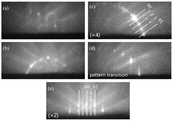
Figure 1.
RHEED patterns of the InP (100) substrate in two azimuthal directions: (a) before the deoxidization process, the surface is spotty; (b) after the deoxidization process, the surface is streaky; (c) a (2 × 4) pattern along the [] crystal orientation with three secondary lines between two primary lines; (d) transition from a (2 × 4) pattern to a (2 × 2) pattern; (e) a (2 × 2) pattern along the [110] crystal orientation with one secondary line between two primary lines.
Epitaxy was then performed in the following order: a lattice-matched buffer layer consisting of 700 nm In0.52Al0.48As was grown at 490 °C with a growth rate of 0.24 μm/h, 100 pairs of alternative 8 nm Be-doped In0.52Al0.48As with a doping concentration of 3.01 × 1019 cm−3, and non-doped 12 nm In0.53Ga0.47As layers were grown on the buffer to form SLs. The growth temperature of SLs was from Tc−280 °C to Tc−250 °C, and the beam equivalent pressure (BEP) of arsenic molecules is 1.35 × 10⁻⁶ Torr. Additionally, the V/III ratio was kept constant at a value of 13 while growing the In0.52Al0.48As buffer, whereas the V/III ratio was 5 while growing SLs due to low substrate temperature.
A combined multilayer structure in this configuration is illustrated in Figure 2a. Typically, when femtosecond fiber lasers with a wavelength of approximately 1.5 μm are incident in the gap of a PCA, photocarriers are generated in the active region. Among the materials that respond to the 1.5 μm wavelength, the ternary alloy InxGa1−xAs is commonly employed as the photoabsorption layer. According to the formula in [20], the bandgap of InGaAs is around Eg~0.751 eV when the In content x = 0.53. However, the inherent features of InGaAs, including the small bandgap and low resistivity, prevent InGaAs from producing a higher photoresponse under strong breakdown voltage. To further increase the dark resistivity and decrease carrier lifetime, the ternary alloy InxAl1−xAs is incorporated to form an alternative-layered structure. Several essential features make InAlAs a key component in fabricating this structure. This ternary alloy has a lattice constant of a = 5.8677 Å when In content x = 0.52, which perfectly matches with InP (a = 5.8687 Å). Meanwhile, InAlAs exhibit higher dark resistivity by two orders of magnitude compared to InGaAs, which significantly reduces the background current when the device is under excitation. Furthermore, photoelectrons can be captured out of the InGaAs layer through a tunneling process and are trapped within the native mid-gap defects, as shown in the mechanism presented in Figure 2b. On this account, the thickness of InxGa1−xAs layers has to be finely considered and grown as thin as possible to enhance the tunneling effect. For our epitaxial samples, 12 nm InGaAs is an adequate thickness. The series of SL samples are then characterized via atomic force microscope (AFM) and X-ray diffraction (XRD) measurements to further discuss the crystalline quality depending on the growth temperature.
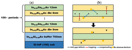
Figure 2.
(a) An illustration of an epitaxy structure on the SI-InP (100) substrate; the multilayered structure in deep blue, light blue, yellow, and green refers to the substrate, buffer layer, and alternative SLs, respectively. (b) An illustration of the electron trapping and compensating mechanism within trapping layers (yellow) and Be atoms (orange).
3. Results and Discussion
The growth of InxAl1−xAs/InxGa1−xAs and GaAs material systems at low temperatures of 150 °C and 200 °C has been investigated in references [15,19]. The observations revealed high resistivity (498 Ω × cm) and high mobility (340 cm2/Vs), resulting in a shorter delay time (300 fs) and a higher dynamic range (70 dB). However, the high density of pyramidal defects and dislocations in the material at the lowest growth temperature of 150 °C resulted in the formation of polycrystalline structures. Moreover, lattice dilation of GaAs grown at a low temperature of 150~200 °C was also observed due to incorporating a high concentration of excess As. These issues will continue to affect the device’s performance unless the growth temperature exceeds 200 °C with promoted crystalline quality. On this account, in our study, growth temperature was set at a range above 200 °C but below 300 °C, aiming to simultaneously acquire the highest resistivity and mobility in SL structures. The substrate temperature was set from 230 °C to 280 °C, and samples grown at 255 °C, 260 °C, 265 °C, and 270 °C were selected to characterize the morphological characteristics. Their unique electrical properties will be further explored in the later discussion. The XRD rocking curves of InP (004) are shown in Figure 3a; it is seen that the arcsec difference between the main 0th InP substrate peak and the InAlAs buffer peak is barely distinguishable in samples grown under 270 °C and 265 °C, which implies the buffer layer is lattice-matched with the substrate and able to offer a flat platform for growing subsequent structures. Though mismatch is still observed in samples grown under 260 °C and 255 °C, it has slight effects in growing the subsequent structure. A fitting curve of the XRD rocking curve is presented at the bottom of Figure 3a; the order number of each peak is clearly shown. The pair of sharp satellite peaks located symmetrically at the sides of the substrate peak is the sixth peak, and the periodic thickness of SLs can be calculated via the following formula,
where D is the periodic length of SLs, λ is the Kα line of the Cu target, θB is the Bragg angle of InP, Δθm is the difference of the Bragg angle corresponding to the difference order number Δm between one satellite peak θm and another satellite peak θm−1, and it is given by
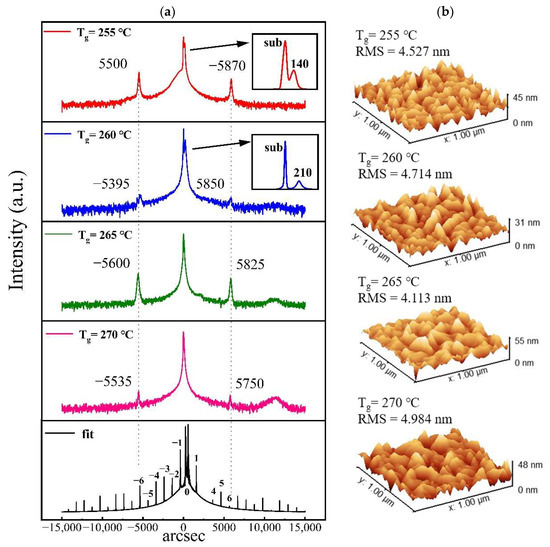
Figure 3.
(a) XRD curves around InP (004) diffraction at the determined temperature region. The mismatch between the sub and buffer is shown in the inset. Δθm is 940.41, 952.08, 937.08, and 947.50 arcsec for samples grown at 270 °C, 265 °C, 260 °C, and 255 °C, respectively. The fit curve is represented, and the satellite peak of each sample corresponds to the peak in the fitted curve. (b) 1 μm2 AFM results in 3D version.
According to the formula above, the periodic length of each sample is 19.85 nm, 19.61 nm, 19.92 nm, and 19.7 nm for samples grown at 270 °C, 265 °C, 255 °C, and 250 °C, respectively. The AFM measurement results are represented in Figure 3b, where the 3D images reveal the rough and uneven interlayer with a root-mean-square (RMS) of 4.527 nm, 4.714 nm, 4.113 nm, and 4.984 nm. The observed roughness can be attributed to the surface mobility reduction during the epitaxy process. In this case, the growth interruption was applied to each epilayer within 5 s to decrease the residence time of surface atoms to fully relax them. Although the crystalline quality is rather poor compared with the morphology obtained above standard temperature (Tg~500 °C), the roughness is sufficient to fabricate photoconductive antennas [21].
High mobility is critical for dynamic range (DNR) performance and operating frequency. A high DNR of 125 at 5 mW was reported in a Fe-doped InGaAs material system [22], and the performance was also optimized through the combination of LTG and Be doping in InGaAs [13]. For InGaAs alloy grown at low temperatures, the thermal excitation of antisite defects under room temperature introduces a significant concentration of mid-gap electron trapping centers which reduce the carrier mobility. By incorporating p-type dopants Be into InGaAs, the compensation effect can effectively decrease the density of carriers generated by ionized AsGa. However, the incorporation of excess Be atoms in InGaAs ionizes AsGa, resulting in the formation of high concentrations of scattering sites and further limiting the carrier transport process. Accordingly, the locally Be-doped profile in the InGaAs/InAlAs multilayered structure expresses doping only in the InAlAs barriers while leaving InGaAs undoped is proposed [15,23]. By doping only in the barrier layer, the concentration of ionized impurity in photoconductive layers is reduced, making it less likely to impede the carrier motion. Such an approach significantly improves the mobility in photoconductive layers; for clarity, the deep-level trapping model and p-doped compensation mechanism are shown in Figure 2b [9,12,24,25]. The variations of the Hall mobility of SL samples are illustrated in Figure 4. This figure not only reveals the correlation between carrier mobility and growth temperature but also depicts its connection with resistivity and carrier concentration as shown in Figure 5. When the temperature ranges between 250 °C and 255 °C, the mobility gradually increases. This rise can be attributed to the compensation of Be at the interface between the InAlAs-InGaAs interface, resulting in a significant amount of ionized defects being balanced, which leads to a notable reduction in carrier concentration, as shown in Figure 5. Thereafter, when the temperature approaches the range from 256 °C to 260 °C, the carrier concentration declines to the lowest level, corresponding to the highest mobility of around 187.2 cm2/Vs. Whereas, after the temperature exceeds 265 °C, the excess Be atoms ionize considerable AsGa and lead to a strong rise of carrier concentration as shown in the curve shown in Figure 5 [13,15]. Therefore, the carrier mobility begins to decline due to the enhanced scattering effect within the InGaAs layer. The study [21] reported a high mobility of 120 cm2/Vs in an undoped InAlAs/InGaAs SLs structure grown on InP (100) at 200 °C, indicating strong electron scattering in this material system.
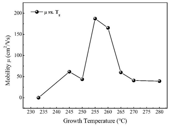
Figure 4.
The carrier mobility versus different growth temperatures characterized at 300 K.
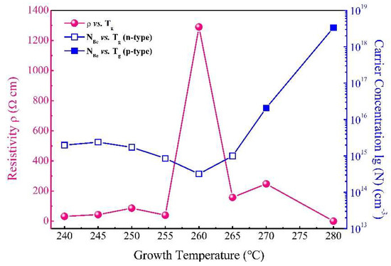
Figure 5.
The relationship between carrier concentration and resistivity depends on the variation of growth temperature.
The curve in Figure 5 compares the relationship between carrier concentration (blue solid and hollow square, right scale) and the Hall resistivity (pink ball, left scale). With an increase in growth temperature, the resistivity gradually rises, reaching approximately 40 Ω × cm at 255 °C. Thereafter, there is a rapid increment, culminating in the peak value of 1290 Ω × cm at around 260 °C, thus more than two times as high as the resistivity of material grown at 150 °C. After reaching the sharp peak, the resistivity decreases rapidly and reaches its lowest point at 280 °C. In line with the trend of the growth temperature, the carrier concentration represents an opposite tendency. It decreases slightly when the growth temperature is set from 240 °C to 255 °C, and the concentration is reduced to the minimum of 3.18 × 1014 cm−3 at 260 °C. It is essential to mention that the carrier concentration increases linearly with temperature until it reaches the maximum at 280 °C. What makes it notable is that the conductivity properties convert at 270 °C from n-type to p-type. In LTG-InGaAs, highly n-conductive performance is mainly attributed to thermal excitation under room temperature. Furthermore, Be atoms incorporated in the InAlAs are distributed at the interlayer between InGaAs and InAlAs, where the dopant concentration is much higher. As a result, high n-type conductivity is exhibited at a growth temperature below 265 °C. However, the transition of conductivity can be attributed to the increased growth temperature above 200 °C; this leads to a higher density of gallium vacancies (VGa), which facilitates the redistribution of AsGa defects [13,19]. Additionally, the crystalline quality of InAlAs continuously promotes as the temperature grows; therefore, the increasing amount of Be atoms is incorporated into the InAlAs lattice and leads to a higher concentration of Be at the InAlAs-InGaAs interface. When the Be concentration and carrier concentration feature the same order, the conductivity transition can be observed. To validate the conductivity transition point, the carrier concentration was calibrated by measuring the Sls sample without the p-doped Be in the InAlAs layer. The result indicates that the background carrier concentration (2.989 1016 cm−3) is in the same order as the carrier concentration at the transition point around 270–280 °C, confirming their strong correlation. Additionally, for growth temperature below 255 °C, the thermal excitation caused high conductivity in InGaAs; hence, the resistivity in these samples is relatively low. However, the growth temperature surpasses 265 °C, and the doping concentration exceeds the carrier density, resulting in the ionization of additional AsGa. As a consequence, the resistivity and carrier concentration both give a reduction, leading to a high conductivity performance. We conclude here that the lowest carrier concentration is responsible for the highest resistivity obtained at a temperature around 257.5–260 °C, and the compensation effect in promoted crystalline quality simultaneously results in the highest mobility.
The current-voltage (I-V) measurements were performed with a probe station. As demonstrated above, the photoresponse of the devices can be influenced by low dark resistance, which further deteriorates their triggering rate. The work presented in [26] evaluated the emission characteristic of a PCA based on a Fe-doped InGaAsP material system, and the researchers showed that the nonuniformity of resistivity is likely caused by the recrystallization process in the InGaAsP/InP heterostructure. This nonuniform resistivity profile deteriorates the performance of the PCA emitter under excitation. Therefore, the PCA emission characteristics can be obtained by evaluating the photocurrent under illumination.
The samples grown at around 260 °C with a resistivity higher than 102 Ω × cm underwent the subsequent semiconductor fabrication process to prepare PCA devices. To begin with, the epitaxial wafer was immersed in acetone and cleaned under ultrasonic waves for 10 min to remove the organic impurities on the surface. Then, a thickness of 800 nm SiO2 film was deposited on the surface using plasma-enhanced chemical vapor deposition (PECVD). The standard lithography was conducted, followed by reactive ion etching (RIE) to form a hard mask. Next, the mesa was formed via one-step inductively coupled plasma (ICP) etching. The hard mask was removed via RIE etching, and a multilayered stack of 400 nm Ti (50 nm)/Pt (50 nm)/Au (300 nm) was deposited on the mesa via physical vapor deposition (PVD) followed by a standard lift-off process to form an ohmic contact. The scanning electron microscopy (SEM) image of the etched mesa with an approximate sidewall depth of 2 μm is shown in Figure 6, meanwhile, a well-fabricated PCA is represented in Figure 7d.
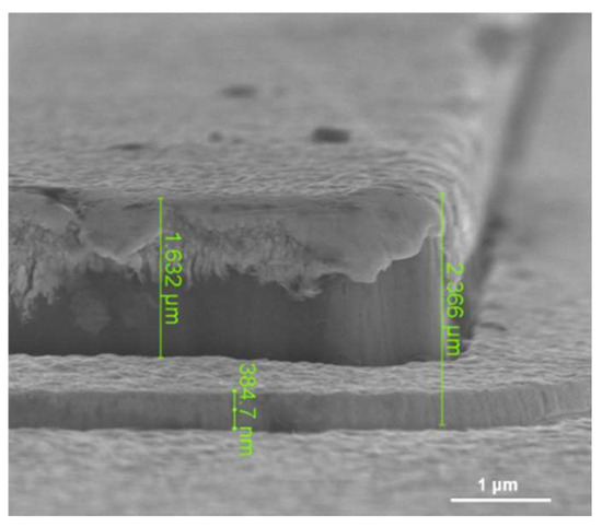
Figure 6.
A SEM image of the etched mesa. The etch depth is 2.366 μm, and the thickness of ohmic contact is 384.7 nm.
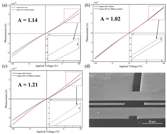
Figure 7.
I-V curves for the three PCAs. The red line refers to the photocurrent obtained under 1500 nm laser excitation, and the blue line refers to the dark current obtained without excitation. The inset shows the enlarged detail of the two curves. (a–c) I-V curves of sample (270 °C), sample (265 °C), sample (260 °C), and (d) SEM image of a fabricated PCA.
The optical fiber is incident at the center of a PCA, and the device is excited via a laser beam with a wavelength of 1500 nm. A DC bias ranging from −10 V to 10 V is applied to the metal contact. Figure 7 shows the dark current and photocurrent measured for all three PCAs. Both the dark current and photocurrent represent a linear against the applied bias, and the photocurrent values are higher than the dark current. This trend is observed from the steeper slope of the curve under excitation compared to the curve obtained under dark conditions. To simplify the explanation, the symbol ‘A’ is introduced to represent the ratio of photoresistance to dark resistance. As shown in the inset of graphs (a) to (c), the value of ratio A is 1.21 for the sample grown at 260 °C, 1.02 for the sample grown at 265 °C, and 1.14 at 270 °C. Based on the data acquired from I-V curves, the highest response was obtained for the sample grown under 260 °C, which partially validates the argument that photocarriers generated with the photoconductive layers encounter less scattering by ionized defects at the optimal growth temperature, resulting in the highest photoresponse under DC bias.
4. Conclusions
This study achieved a balance between high resistivity and high carrier mobility in the InAlAs:Be/InGaAs superlattice utilizing the LTG method. The optimal electrical performance was observed in samples grown at 260 °C, exhibiting the highest resistivity, mobility, and the lowest carrier concentration. To further assess the crystalline quality, four samples were selected for XRD analysis. The results confirmed that the periodic length of these samples matched the expected values, indicating the relatively high crystal quality when utilizing the LTG method. On the other hand, the Hall effect test revealed that temperature exceeding 265 °C resulted in the incorporation of excessive Be atoms in the active layer and ionization of excess defects. This process leads to a decline in resistivity and mobility, disrupting the delicate equilibrium between mobility, concentration, and resistivity. Moreover, several PCAs were prepared for photoresponse measurement, and the highest photoresponse was obtained at the optimal temperature of 260 °C. According to our investigation, the optimal growth temperature for LTG-InAlAs:Be/InGaAs SLs is within the range of 257.5–260 °C.
Author Contributions
Conceptualization, H.N.; methodology, H.N.; investigation, X.S. (Xiangjun Shang), X.S. (Xiangbin Su) and S.L.; optical measurement, D.D.; sample growth, D.D., H.L. and X.S. (Xiangbin Su); writing−original draft preparation, D.D. and H.L.; writing−review and editing, D.D. and H.L.; supervision, H.N. and Z.N.; funding acquisition, H.N. and Z.N. The authors also appreciate Cheng-ao Yang and Faran Chang for polishing the manuscript. All authors have read and agreed to the published version of the manuscript.
Funding
This research was funded by the National Natural Science Foundation of China (Grant Nos. 62035017, 61505196), the National Key Technologies R&D Program of China (Grant No. 2018YFA0306100), and the Key-Area Research and Development Program of Guangdong Province (Grant No. 2018B030329001).
Data Availability Statement
The data that support the findings of this study are available from the corresponding author upon reasonable request.
Conflicts of Interest
The authors declare no conflict of interest.
References
- Hashimshony, D.; Geltner, I.; Cohen, G.; Avitzour, Y.; Zigler, A.; Smith, C. Characterization of the electrical properties and thickness of thin epitaxial semiconductor layers by THz reflection spectroscopy. J. Appl. Phys. 2001, 90, 5778–5781. [Google Scholar] [CrossRef]
- Federici, J.F.; Schulkin, B.; Huang, F.; Gary, D.; Barat, R.; Oliveira, F.; Zimdars, D. THz imaging and sensing for security applications—Explosives, weapons and drugs. Semicond. Sci. Technol. 2005, 20, S266. [Google Scholar] [CrossRef]
- Jacobsen, R.H.; Mittleman, D.M.; Nuss, M.C. Chemical recognition of gases and gas mixtures with terahertz waves. Opt. Lett. 1996, 21, 2011–2013. [Google Scholar] [CrossRef] [PubMed]
- Ashworth, P.C.; Pickwell-MacPherson, E.; Provenzano, E.; Pinder, S.E.; Purushotham, A.D.; Pepper, M.; Wallace, V.P. Terahertz pulsed spectroscopy of freshly excised human breast cancer. Opt. Express 2009, 17, 12444–12454. [Google Scholar] [CrossRef] [PubMed]
- Smith, P.R.; Auston, D.H.; Nuss, M.C. Subpicosecond photoconducting dipole antennas. IEEE J. Quantum Electron. 1988, 24, 255–260. [Google Scholar] [CrossRef]
- Auston, D.H.; Cheung, K.P.; Valdmanis, J.A.; Kleinman, D.A. Cherenkov Radiation from Femtosecond Optical Pulses in Electro-Optic Media. Phys. Rev. Lett. 1984, 53, 1555–1558. [Google Scholar] [CrossRef]
- Gupta, S.; Frankel, M.Y.; Valdmanis, J.A.; Whitaker, J.F.; Mourou, G.A.; Smith, F.W.; Calawa, A.R. Subpicosecond carrier lifetime in GaAs grown by molecular beam epitaxy at low temperatures. Appl. Phys. Lett. 1991, 59, 3276–3278. [Google Scholar] [CrossRef]
- Salem, B.; Morris, D.; Aimez, V.; Beerens, J.; Beauvais, J.; Houde, D. Pulsed photoconductive antenna terahertz sources made on ion-implanted GaAs substrates. J. Phys. Condens. Matter 2005, 17, 7327. [Google Scholar] [CrossRef]
- Sartorius, B.; Roehle, H.; Künzel, H.; Böttcher, J.; Schlak, M.; Stanze, D.; Venghaus, H.; Schell, M. All-fiber terahertz time-domain spectrometer operating at 1.5 µm telecom wavelengths. Opt. Express 2008, 16, 9565–9570. [Google Scholar] [CrossRef]
- Ueda, O.; Ikenaga, N.; Hirose, S.; Hirayama, K.; Tsurisaki, S.; Horita, Y.; Tominaga, Y. Structural evaluation of low-temperature-grown InGaAs crystals on (001) InP substrates. J. Cryst. Growth 2020, 548, 125852. [Google Scholar] [CrossRef]
- Jooshesh, A.; Fesharaki, F.; Bahrami-Yekta, V.; Mahtab, M.; Tiedje, T.; Darcie, T.E.; Gordon, R. Plasmon-enhanced LT-GaAs/AlAs heterostructure photoconductive antennas for sub-bandgap terahertz generation. Opt. Express 2017, 25, 22140–22148. [Google Scholar] [CrossRef] [PubMed]
- Gregory, I.S.; Tey, C.M.; Cullis, A.G.; Evans, M.J.; Beere, H.E.; Farrer, I. Two-trap model for carrier lifetime and resistivity behavior in partially annealed GaAs grown at low temperature. Phys. Rev. B 2006, 73, 195201. [Google Scholar] [CrossRef]
- Globisch, B.; Dietz, R.J.B.; Stanze, D.; Göbel, T.; Schell, M. Carrier dynamics in Beryllium doped low-temperature-grown InGaAs/InAlAs. Appl. Phys. Lett. 2014, 104, 172103. [Google Scholar] [CrossRef]
- Globisch, B.; Dietz, R.J.B.; Nellen, S.; Göbel, T.; Schell, M. Terahertz detectors from Be-doped low-temperature grown InGaAs/InAlAs: Interplay of annealing and terahertz performance. AIP Adv. 2016, 6, 125011. [Google Scholar] [CrossRef]
- Kohlhaas, R.B.; Dietz, R.J.B.; Breuer, S.; Nellen, S.; Liebermeister, L.; Schell, M.; Globisch, B. Improving the dynamic range of InGaAs-based THz detectors by localized beryllium doping: Up to 70 dB at 3 THz. Opt. Lett. 2018, 43, 5423–5426. [Google Scholar] [CrossRef]
- Takahashi, R.; Kawamura, Y.; Kagawa, T.; Iwamura, H. Ultrafast 1.55-μm photoresponses in low-temperature-grown InGaAs/InAlAs quantum wells. Appl. Phys. Lett. 1994, 65, 1790–1792. [Google Scholar] [CrossRef]
- Dietz, R.J.B.; Globisch, B.; Gerhard, M.; Velauthapillai, A.; Stanze, D.; Roehle, H.; Koch, M.; Göbel, T.; Schell, M. 64 μW pulsed terahertz emission from growth optimized InGaAs/InAlAs heterostructures with separated photoconductive and trapping regions. Appl. Phys. Lett. 2013, 103, 061103. [Google Scholar] [CrossRef]
- Nandi, U.; Dutzi, K.; Deninger, A.; Lu, H.; Norman, J.; Gossard, A.C.; Vieweg, N.; Preu, S. ErAs:In(Al)GaAs photoconductor-based time domain system with 4.5 THz single shot bandwidth and emitted terahertz power of 164 µW. Opt. Lett. 2020, 45, 2812–2815. [Google Scholar] [CrossRef]
- Luysberg, M.; Sohn, H.; Prasad, A.; Specht, P.; Liliental-Weber, Z.; Weber, E.R.; Gebauer, J.; Krause-Rehberg, R. Effects of the growth temperature and As/Ga flux ratio on the incorporation of excess As into low temperature grown GaAs. J. Appl. Phys. 1998, 83, 561–566. [Google Scholar] [CrossRef]
- Nee, T.W.; Green, A.K. Optical properties of InGaAs lattice-matched to InP. J. Appl. Phys. 1990, 68, 5314–5317. [Google Scholar] [CrossRef]
- Galiev, G.B.; Vasiliev, A.L.; Vasil’evskii, I.S.; Vinichenko, A.N.; Klimov, E.A.; Klochkov, A.N.; Trunkin, I.N.; Pushkarev, S.S. Structural Characteristics of Epitaxial Low-Temperature Grown {InGaAs/InAlAs} Superlattices on InP(100) and InP(111)A Substrates. Crystallogr. Rep. 2020, 65, 496–501. [Google Scholar] [CrossRef]
- Hatem, O.; Cunningham, J.; Linfield, E.H.; Wood, C.D.; Davies, A.G.; Cannard, P.J.; Robertson, M.J.; Moodie, D.G. Terahertz-frequency photoconductive detectors fabricated from metal-organic chemical vapor deposition-grown Fe-doped InGaAs. Appl. Phys. Lett. 2011, 98, 121107. [Google Scholar] [CrossRef]
- Kohlhaas, R.B.; Nellen, S.; Liebermeister, L.; Globisch, B.; Schell, M. 70 dB signal-to-noise ratio at 3 THz using locally doped InGaAs-based photoconductive detectors. In Proceedings of the 2017 42nd International Conference on Infrared, Millimeter, and Terahertz Waves (IRMMW-THz), Cancun, Mexico, 27 August–1 September 2017; pp. 1–2. [Google Scholar]
- Burford, N.; El-Shenawee, M. Review of terahertz photoconductive antenna technology. Opt. Eng. 2017, 56, 010901. [Google Scholar] [CrossRef]
- Yachmenev, A.E.; Pushkarev, S.S.; Reznik, R.R.; Khabibullin, R.A.; Ponomarev, D.S. Arsenides-and related III-V materials-based multilayered structures for terahertz applications: Various designs and growth technology. Prog. Cryst. Growth Charact. Mater. 2020, 66, 100485. [Google Scholar] [CrossRef]
- Petrov, B.; Fekecs, A.; Sarra-Bournet, C.; Arès, R.; Morris, D. Terahertz Emitters and Detectors Made on High-Resistivity InGaAsP:Fe Photoconductors. IEEE Trans. Terahertz Sci. Technol. 2016, 6, 747–753. [Google Scholar] [CrossRef]
Disclaimer/Publisher’s Note: The statements, opinions and data contained in all publications are solely those of the individual author(s) and contributor(s) and not of MDPI and/or the editor(s). MDPI and/or the editor(s) disclaim responsibility for any injury to people or property resulting from any ideas, methods, instructions or products referred to in the content. |
© 2023 by the authors. Licensee MDPI, Basel, Switzerland. This article is an open access article distributed under the terms and conditions of the Creative Commons Attribution (CC BY) license (https://creativecommons.org/licenses/by/4.0/).