Abstract
The selection of the π-conjugation spacers in semi-conducting polymer backbone is one of the important factors for determining the optoelectrical and morphological properties in organic photodiodes. To study the effects of π-conjugation spacers in donor–acceptor (D-A)-type alternating copolymers on their device performances in all-polymer-based photodiodes (all-PPDs), a series of diketopyrrolopyrrole (DPP)-based copolymers as polymer donors (PDs) were designed and synthesized. In detail, three different π-conjugation spacers, thiophene (T for P1), thienothiophene (TT for P2), and bithiophene (BT for P3), were incorporated into the DPP-based copolymer structures. Interestingly, all-PPDs based on the series of P1–P3 as PDs and N2200 as a polymer acceptor (PA) exhibited totally distinct device performances in terms of external quantum efficiency (EQE), dark current density (JD), and ideal detectivity (D*). The P1-based device showed suppressed JD (6.1 × 10⁻¹¹ A/cm2 at −1 V) compared to those of the P2- and P3-based devices due to the lower lying of the highest occupied molecular orbital (HOMO) level of P1. However, the P3-based all-PPD showed higher EQE (16% at 630 nm wavelength and −1 V) compared to those of the P1- and P2-based devices. And, it mainly originated from the better molecular packing and final blend film morphology, as confirmed by morphological analyses.
1. Introduction
Organic photodetectors (OPDs) are optoelectronic devices that can convert optical signals into electrical signals. They find applications in various fields such as biomedical imaging, environmental monitoring, and military guidance. OPDs have been extensively studied and developed due to their advantages, including solution processability, lightweight nature, low cost, and the ability to fabricate large-area devices [1,2,3,4,5,6,7,8]. Among the different types of photo-active materials, all-PPDs have emerged as a promising next-generation technology due to the following reasons: (i) Device performance: These all-PPDs utilize both a polymer donor (PD) and a polymer acceptor (PA) in their active layers, while conventional OPDs generally utilize the fullerene-based acceptors. Thus, all-PPDs can exhibit superior light-harvesting ability, which can provide higher photocurrent relative to conventional OPDs. (ii) Mechanical stability: The replacement of fullerene acceptors with PAs can significantly improve mechanical properties due to the entanglement effects of polymer chains [9,10,11,12]. This enables the development of wearable and stretchable OPDs, further expanding their potential in emerging fields [13]. To achieve high-performance all-PPDs, two key factors are crucial: the development of new photo-active polymers and the optimization of the bulk-heterojunction (BHJ) film morphology [14,15,16]. The D-A approach, in which a perfectly alternating pattern of covalently bound electron-rich and electron-poor chemical units (push–pull) comprises the backbone, is frequently adopted to obtain PD or PA for the fabrication of organic photoelectronic devices such as OPDs [17], organic photovoltaics (OPVs) [18] and organic field-effect transistors (OFETs) [19,20]. The DPP unit has a strong electron-withdrawing structure, and DPP-based D-A copolymers typically show excellent optical and electrical properties due to their strong and broad absorption and high charge carrier mobility [17,18,19,20]. However, these DPP-based copolymers have been less studied in terms of investigating the relationship between PD structure and device performance in all-PPDs.
In this study, we synthesized new D-A-type copolymers based on DPP by incorporating three different aromatic (Ar) linkers (thiophene (T), thienothiophene (TT), and bithiophene (BT)) into the polymer main backbone. Specifically, we utilized benzodithiopene (BDT) as the donor moiety to construct the alternating copolymers Ar-DPP-Ar-BDT, where Ar represents the specific linker (T for P1, TT for P2, and BT for P3). To assess the influence of the Ar linkers on the performance of PD in all-PPDs, we employed poly{[N,N0-bis(2-octyldodecyl)-naphthalene-1,4,5,8-bis(dicarboximide)-2,6-diyl]-alt-5,50-(2,20-bithiophene)} as the PA. The incorporation of Ar linkers into the PDs greatly affected not only their electronic energy levels but also the blend film morphologies when mixed with N2200 PA. And these effects resulted in totally different ideal detectivity (D*) in the series of P1-, P2-, and P3-based all-PPDs.
2. Materials and Methods
2.1. Materials
3,6-Bis(5-bromothiophen-2-yl)-2,5-bis(2-decyltetradecyl)pyrrolo[3,4-c]pyrrole-1,4(2H,5H)-dione (Br-T-DPP-T-Br), 3,6-bis(5-bromothieno[3,2-b]thiophen-2-yl)-2,5-bis(2-decyltetradecyl)-2,5-dihydropyrrolo[3,4-c]pyrrole-1,4-dione (Br-TT-DPP-TT-Br), 3,6-bis(5’-bromo-[2,2′-bithiophen]-5-yl)-2,5-bis(2-decyltetradecyl)-2,5-dihydropyrrolo[3,4-c]pyrrole-1,4-dione (Br-BT-DPP-BT-Br), (4,8-bis(4,5-dioctylthiophen-2-yl)benzo[1,2-b:4,5-b′]dithiophene-2,6-diyl)bis(trimethylstannane) (Tin-BDT-Tin), and other chemicals were purchased from Sunatech Incorporation(Jiangsu, China), Organtec Ltd. (Beijing, China), Derthon (Shenzhen, China), Sigma Aldrich Co. (Seoul, South Korea), and Tokyo Chemical Industry Co. (Seoul, South Korea). N2200 as a PA was purchased from eFlexPV (Futian, Hong Kong). All materials and reagents were used without further purification.
2.2. Synthesis
Synthesis of P1: Br-T-DPP-T-Br (169.7 mg, 0.15 mmol), Tin-BDT-Tin (169.3 mg, 0.15 mmol), and tetrakis(triphenylphosphine)palladium(0) Pd(PPh3)4 (10.4 mg, 6 mol%) were dissolved into 5 mL of toluene and 1 mL of dimethylformamide (DMF) in a round flask. The solution was flushed with nitrogen for 10 min and then sealed. Then, the polycondensation reaction proceeded at 110 °C for 24 h. The reaction was cooled to room temperature and precipitated in methanol. The precipitate was filtered and subjected to Soxhlet extraction with methanol, acetone, hexane, methylenechloride (MC), and chloroform (CF) in sequence. The fractions extracted by MC and CF were precipitated with methanol and then filtered. The polymers were dried under vacuum. The yield of polymers was 135 mg (MC) and 65 mg (CF). The MC fraction was used for all characterization and device fabrication.
Synthesis of P2: P2 was prepared using the same procedure and reaction conditions as for P1. The yield of polymers was 224 mg (MC) and 15 mg (CF). The CF fraction was used for all characterization and device fabrication.
Synthesis of P3: P3 was prepared using the same procedure and reaction conditions as for P1 and P2. The yield of polymers was 34 mg (MC) and 246 mg (CF). The CF fraction was used for all characterization and device fabrication.
2.3. Fabrication and Characterization of All-PPDs
Our inverted-type all-PPD device configuration follows the structure indium tin oxide (ITO)/pixel define layer (PDL)/zinc oxide (ZnO)/(P1, P2, and P3):N2200/molybdenum trioxide (MoO3)/silver (Ag). The ZnO was prepared through a sol–gel procedure by dissolving 1 g of zinc acetate dihydrate (Zn(O2CCH3)2·(H2O)2, 99.9%) and 0.28 g of ethanolamine (HOCH2CH2NH2, 99.5%) in 10 mL of anhydrous 2-methoxy ethanol (CH3OCH2CH2OH, >99.8%). This mixture was vigorously stirred over 24 h to facilitate the hydrolysis reaction and aging to process. ZnO thin films with a thickness of 30 nm were formed by spin-coating the sol–gel precursor solution at 3000 rpm onto the ITO substrate, followed by heating at 200 °C for 1 h in an air environment. After applying the ZnO layer, all subsequent procedures were conducted within a glove box under a N2 atmosphere. Each blended solution was spin-cast onto an ITO/ZnO substrate at 1000 rpm for 90 s. The final thickness of each film was in the range of 110~120 nm. Subsequently, the substrates were introduced into an evaporation chamber and maintained under high vacuum conditions (below 10−6 Torr) over 1 h before depositing around 10 nm of MoO3 and 100 nm of Ag. The active area of the fabricated devices measured 0.09 cm2. For the assessment of current density–voltage (J–V) characteristics, the OPDs were evaluated using a Keithley 4200 semiconductor parameter analyzer. The external quantum efficiency (EQE) spectra were acquired using a spectral photon-to-electron conversion efficiency measurement system, illuminated by monochromatic light generated by an ozone-free Xe lamp equipped with an optical filter (chopper frequency: 50 Hz).
2.4. Other Characterizations
The nuclear magnetic resonance (NMR) was measured with Bruker AVANCE III HD 500 in CDCl3 solvent at room temperature. The molecular weight (Mn) and polydispersity (Ð) of the polymers used in this study were measured using gel permission chromatography (GPC, Agilent PL-GPC220) eluted with 1,2,4-trichlorobenzene (TCB) heated to 160 °C and a flow rate of 1 mL min-1 relative to polystyrene-divinylbenzene. The GPC column was bought from Tosoh Bioscience LLC (Model: TSKgel GMHHR-H (S) HT2). The thermal properties of polymers from 20 to 300 °C were measured with DSC (TA Discovery) at a rate of 10 °C min−1, and the reported values are from the second heating/cooling cycle. UV–visible (UV–vis) absorption spectra were acquired using a UV-1800 spectrophotometer (Shimadzu Scientific Instruments) at room temperature.
Grazing incidence X-ray scattering (GIXS) measurements were conducted at beamline 9A in the Pohang Accelerator Laboratory (Pohang, South Korea). GIXS samples were prepared by the spin-coating of all-polymer blends or polymer-only solutions (~10 mg/mL) in chloroform (CF) onto a SiO2 substrate at 1000 rpm for 40 s. An incidence angle of approximately 0.12° was selected to ensure complete X-ray penetration into the film. In addition, exposure time was 5 s for all samples. Atomic force microscopy (AFM) measurements were carried out using a Veeco Dimension 3100 instrument in tapping mode.
3. Results and Discussion
3.1. Synthesis and Characterization of PDs and PA
For this study, three PDs were designed and synthesized based on the same polymer backbone. Specifically, different Ar linkers of T, TT, and BT were incorporated onto an Ar-DPP-Ar-BDT backbone with a polycondensation reaction based on Stille coupling to yield P1, P2, and P3, respectively (see Figure 1a). In addition, 6 mol% of Pd(PPh3)4 catalyst was used for the polymerization of the three PDs. The synthesis procedures for monomer preparation and polymerization, along with their NMR and GPC characterizations, are described in the Supporting Information (Figures S1–S3). Additionally, N2200 was purchased from eFlexPV and used as a PA in this study. Figure 1 shows the chemical structures, thin-film UV–vis absorption spectra, and energy-level alignment diagrams of P1, P2, P3, and N2200. Basic information on the three PDs and PA, including molecular weight and electrochemical and optical properties, is summarized in Table 1. P1 (extracted from MC), P2 (extracted from CF), and P3 (extracted from CF) had similar average molecular weights (Mn) in the range of 40~60 kg mol–1, minimizing the influence of molecular weight on their properties (Table S1).
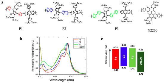
Figure 1.
(a) Molecular structure, (b) thin-film UV–vis spectra, and (c) energy levels of P1, P2, and P3 as PDs and N2200 as a PA.

Table 1.
Material properties of P1, P2, and P3 as PDs and N2200 as a PA used in this study.
The thin-film UV–vis absorption spectra of the P1, P2, and P3 as PDs and N2200 as a PA are presented in Figure 1b. These three polymers exhibit similar absorption onsets at ca. 830 nm, corresponding to an optical band gap (Eg) of 1.5 eV. The maximum absorption peak (λmax) of P1 was at around 765 nm, while P2 and P3 displayed absorption peaks at approximately 758 nm and 750, respectively. Additionally, each PD exhibited a different intensity ratio between two vibronic peaks (A0-0/A0-1). (P1: 1.65, P2: 1.51, and P3: 1.29.) Thus, the incorporation of different Ar linkers in PDs can influence the PD aggregation behaviors in the film states [21,22].
The highest occupied molecular orbital (HOMO) levels of P1, P2, and P3 were measured with photoelectron spectroscopy (AC3, RIKEN KEIKI), while the lowest unoccupied molecular orbital (LUMO) levels were calculated using their optical bandgaps (Table 1). The HOMO/LUMO levels of P1 were found to be −3.60 eV and –5.43 eV, respectively, showing a down-shift compared to both P2 and P3. This down-shift is primarily attributed to the decreased electron density of T linker in P1 when compared to both TT and BT linkers [23]. To further support the observed differences in HOMO levels of each PD, density functional theory (DFT) was employed at the B3LYP/6-311G(d,p) level (Figure S4). These calculations were simplified by using the D-A monomer of each PD and methyl groups in place of the branched alkyl chains on both DPP and BDT moieties. The simulated energy level trends were well matched with corresponding experimental values. Accordingly, it is expected that P1-based all-PPD devices will exhibit a lower dark current density (JD) compared to both P2- and P3-based devices [24]. The thermal properties of the three PDs were characterized with DSC (see Figure S5). However, no clear thermal transitions were observed with DSC, which is consistent with other PDPP-BDT derivatives previously reported in the literature [25].
3.2. All-PPD Device Characterization
We characterized the photoelectric properties of three PDs in all-PPD structures with layers of ITO/PDL/ZnO/active layers (P1:N2200, P2:N2200, and P3:N2200)/MoO3/Ag (Figure 2a). The active layers were directly spin-coated on top of the ZnO layer, followed by the thermal deposition of MoO3/Ag layers. The device fabrication procedure is described in more detail in the experimental section. The optimized blend ratio of PD/PA was 1:1 (w/w), and the optimized film thickness of the active layer spun-cast from a chloroform (CF) solution was approximately 120 nm for all PD types.
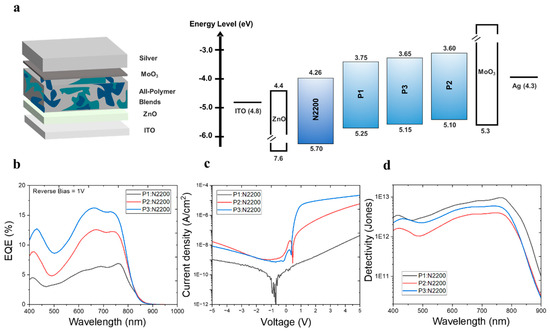
Figure 2.
(a) Inverted-type device structure of all-PPDs used in this study, (b) EQE spectra under reverse bias of 1 V, (c) voltage–dark current density curves, and (d) ideal detectivity spectra under reverse bias of 1 V of three different systems (P1:N2200, P2:N2200, and P3:N2200).
In a device with P3, the external quantum efficiency (EQE) measured at a reverse bias of 1 V in the visible range was higher than that in devices with other PDs. (Figure 2b). The wavelength at maximum EQE (λEQE,max) was 660 nm for P1, 670 nm for P2, and 760 nm for P3. In addition, when comparing the bias dependency (reverse bias range = 0~5 V) of EQE of the three all-PPD devices, similar trends were clearly observed (Figure S6). Thus, the EQE gradually decreased in the order of P3, P2, and P1. Despite the decrease in EQE in devices with P1 compared to those with P2 and P3, the significantly reduced JD contributed to the improved D*, which was calculated as (EQE/1240 × λ)/(2qJD)0.5, where λ is the target wavelength and q is the electric charge [26]. For example, in the comparison between the devices with P1 and P3, the EQE decreased from 15.6% to 6.4%. However, as shown in Figure 2c, the JD was also suppressed by 12.5 times, from 7.6 × 10⁻¹⁰ to 6.1 × 10⁻¹¹ A/cm2. Considering the similarity of active layer thicknesses between the three different all-PPD devices, this suppression mainly originated from the deeper HOMO level of P1 compared to those of the other PDs. Thus, the presence of the lower-lying HOMO level of P1 in the all-PPD device may effectively suppress undesired charge injection under a reverse bias, resulting in an extremely low JD [24,27]. Consequently, D* increased from 5.9 × 10¹² (λEQE,max = 660 nm) for P1 to 8.5 × 10¹² Jones (λEQE,max = 760 nm) for P3 (Figure 2d). However, in the P2-based device, the D* (3.8 × 10¹² at λEQEmax = 670 nm) was lower than those of both P1 and P3, mainly owing to both the lower EQE and the higher JD. When observing the reverse scan of I-V curves in the dark condition, similar trends of JDs were observed in all PD types of the all-PPDs. In addition, the trends of photo current levels under white light illumination in three PD-based all-PPDs were well matched with their EQE levels in the order of P1-, P2-, and P3-based all-PPDs (Figure S7). The effects of the PD:PA ratio (2:1, 1:1, and 1:2) on the EQE levels in all-PPDs with three PDs were further investigated. As shown in Figure S8, the optimized values of EQE were achieved in all PD types of all-PPDs when the PD:PA ratio reached 1:1. To further investigate the effects of Ar linkers in PDs on the electrical performance, the device absorption (nA) was measured using reflectance, and their corresponding internal quantum efficiency (IQE) was calculated according to the equation IQE(λ) = EQE(λ)/nA(λ) [13]. As shown in Figure S9, all-PPDs with different PDs showed very similar nA (82~87%) in the range of 650~750 nm wavelengths. Thus, the origins the of EQE trends were determined by their corresponding IQE values.
3.3. Morphology Characterization
To gain a fundamental understanding of the effect of the structural changes in PDs on their photoelectrical characteristics in all-PPDs, we examined the microstructure and blend morphology of the P1:N2200, P2:N2200, and P3:N2200 films using GIXS and AFM measurements. First, the GIXS results of the pristine P1, P2, and P3 films were compared (Figure 3a,b and Figure S10 and Table 2). All of the PDs had pronounced (100) scattering peaks in the in-plane direction (qxy), but their peak positions differed, corresponding to different lamellar spacings of 23.1, 24.7, and 24.4 Å for P1, P2, and P3, respectively.
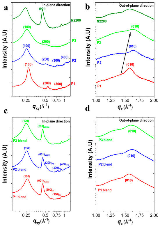
Figure 3.
2D-GIXS linecut profiles of pristine polymer (a,b) and blend films (c,d) in the (a,c) in-plane and (b,d) out-of-plane directions.
Table 2.
Detailed GIXS (100) peak information for IP direction and (010) peak information for OOP direction of pristine films.
Additionally, the P1 and P2 films showed highly ordered structures up to the third-order (300) peaks and fourth-order (400) peaks, respectively, while P3 exhibited no high-order peaks (i.e., (300) and (400)). Furthermore, when evaluating the crystalline order with calculations of the crystalline correlation length (D100) of the polymers using the Scherrer equation [28], the D100 value significantly increased from 8.29 nm (P3) to 10.71 nm (P2) to 20.67 nm (P1). Therefore, the incorporation of different Ar linkers in the Ar-DPP-Ar-BDT backbone significantly affected the crystalline ordering of PDs in thin films. Additionally, the GIXS patterns provide important insights into the π-π stacking behavior of the PD series in thin films. Although all pristine films had a preferential face-on molecular orientation, they exhibited a significant difference in π-stacking distance. The corresponding distances were 3.99 Å for P1, 3.79 Å for P2, and 3.80 Å for P3. Hence, the shorter π-stacking distance in both P2 and P3 could enhance charge transport by reducing the energy barriers for charge hopping/transfer between adjacent molecules [29].
Figure 3c,d and Figure S10e,g compare the GIXS patterns of three PDs:N2200 blends under optimized device conditions, revealing similar trends in π-stacking distance and crystalline orientation in PDs/N2200 blend films. Notably, while the P3/N2200 blend exhibited a single (100)in diffraction peak, both the P1- and P2-based blend films still displayed high-order peaks up to the fourth-order (400)in peaks. This phenomenon in both the P1- and P2-based blends was also observed in highly crystalline all-polymer blends, such as P3HT:N2200 [30] and PPDT2FBT:N2200 [31].
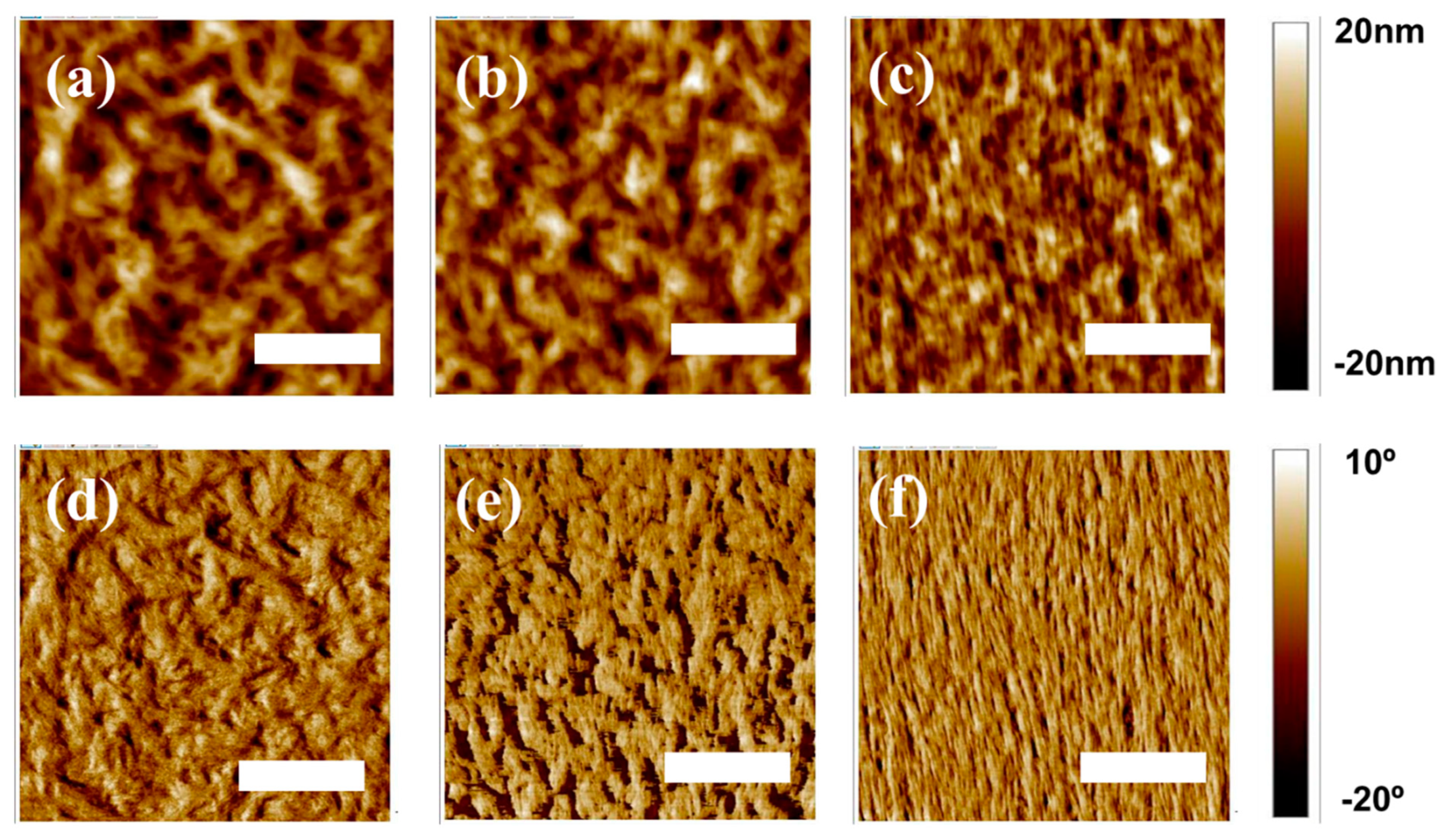
These differences in the tendency for the formation of pure PD crystalline phase in the three different PD:N2200 blends were further investigated by visualizing the AFM images. As shown in Figure 4, distinct domain sizes in the PDs:N2200 blends were evident. Figure 4a,b (or Figure 4d,e) display large aggregates with significantly reduced interfacial areas in both P1- and P2-based blends, which contrasts starkly with the notably finer domains of the P3:N2200 blend (Figure 4c), indicating clear suppression of macroscopic phase separation in the P3:N2200 blend.

Figure 4.
AFM topographical images (3 × 3 μm2) of the surfaces of all-polymer blends, (a) P1:N2200, (b) P2:N2200, and (c) P3:N2200, and the corresponding phase images of (d) P1:N2200, (e) P2:N2200, and (f) P3:N2200 (scale bars: 1 μm).
Moreover, the root-mean-square (rms) roughness of the P3:N2200 blend was lower than those of both the P1- and P2-based blends (P1 for 11.8 nm, P2 for 11.4 nm, and P3 for 5.6 nm). Thus, a lower tendency of self-aggregation behavior in P3 may facilitate intermixing with N2200 PA in the P3:N2200 blend film, potentially enhancing exciton dissociation and charge generation [31,32]. Consequently, not only the narrower π-stacking distance but also the final blend morphology in the P3:N2200 blend may contribute to increased photoelectrical properties compared to those of both the P2- and P1-based blends.
Our work shows sufficiently high D* values near 1013 Jones when comparing the device performances with those of previously reported all-polymer-based OPD systems (Table S2) [16,33,34,35,36,37,38], and this was mainly due to the (1) deeper HOMO level of PD which can provide an excessively low JD less than 0.1 nA/cm2 and (2) finer blend morphology in PD/PA blends which can ensure an efficient charge separation process.
4. Conclusions
In summary, we successfully synthesized new D-A-type copolymers based on an Ar-DPP-Ar-BDT backbone by incorporating three different Ar linkers (Ar = T, TT, and BT) into the polymer main backbone. The introduction of Ar linkers into the PDs significantly impacted their HOMO energy levels, consequently influencing the level of JD in all-PPDs. Furthermore, the three PDs exhibited distinct blend film morphologies in terms of domain size, crystallinity, and crystal orientation when combined with N2200 PA, as evidenced by morphological investigations. Our work demonstrates an important material design strategy to control both the energy level and the crystallinity of PDs, applicable in highly efficient all-PPDs: (i) In terms of energy level, lowering the HOMO level of PD is important for suppressing the JDs. (ii) In terms of crystallinity, developing highly crystalline PDs should be avoided to suppress severe phase separation in the PD/N2200 blend system.
Supplementary Materials
The following supporting information can be downloaded at: https://www.mdpi.com/article/10.3390/cryst13101454/s1, Figure S1: Synthetic procedures for P1, P2 and P3; Figure S2: NMR characterizations of monomers (a–h) and polymers (i–k) used in this study; Figure S3: GPC profiles of three PDs (P1, P2, and P3); Figure S4: DFT calculation for estimation of HOMO/LUMO levels of P1, P2 and P3 polymers; Figure S5: DSC measurements for P1, P2 and P3 (a) 2nd cycle of heating, (b) 2nd cycle of cooling; Figure S6: EQE vs bias dependency of P1 (a), P2 (b), and P3-based all-PPD devices (c); Figure S7: J-V curves of three PDs based all-PPDs under the dark condition (forward and reverse scan) and under the white light; Figure S8: EQE curves of three PDs based all-PPDs with different PD:PA weight ratios (reverse bias = −1V); Figure S9: (a) Device absorption spectrums, and (b) IQE spectrums (reverse bias = 1V) of P1, P2, and P3 based all-PPDs; Figure S10: GIXD reciprocal mapping images of pure polymers and all-polymer blends. (a) P1, (b) P2, (c) P3, (d) N2200; (e) P1:N2200, (f) P2:N2200, (g) P3:N2200; Table S1: Material information of three PDs used in this study (Amount, Mn, Mw, and PDI); Table S2: Comparison of our work with representative OPDs based on all-polymer-based photo-active materials.
Author Contributions
H.K. (Hyunbum Kang), H.K. (Hyungjun Kim), Y.Y. and G.H.L. conceived and designed the experiments. H.K. (Hyunbum Kang), H.K. (Hyungjun Kim) and A.C. contributed to the analysis and discussion of results. Y.Y. and G.H.L. supervised the project. H.K. (Hyunbum Kang), H.K. (Hyungjun Kim), G.H.L. and Y.Y. organized the data and wrote this manuscript. All authors have read and agreed to the published version of the manuscript.
Funding
This work was supported by the National Research Foundation of Korea (NRF) grant funded by the Korea government (MSIT) (No. 2022R1A5A8019303).
Data Availability Statement
Not applicable.
Acknowledgments
We gratefully acknowledge the provision of beamtime at the 9A U-SAXS Beamline at the Pohang Accelerator Laboratory (South Korea). We would like to thank Hyungju Ahn for helpful discussion on the GIWAXS data analysis.
Conflicts of Interest
The authors declare no competing financial interest.
References
- Lee, Y.; Chung, J.W.; Lee, G.H.; Kang, H.; Kim, J.-Y.; Bae, C.; Yoo, H.; Jeong, S.; Cho, H.; Kang, S.-G.; et al. Standalone real-time health monitoring patch based on a stretchable organic optoelectronic system. Sci. Adv. 2021, 7, eabg9180. [Google Scholar] [CrossRef] [PubMed]
- Lee, G.H.; Kang, H.; Chung, J.W.; Lee, Y.; Yoo, H.; Jeong, S.; Cho, H.; Kim, J.-Y.; Kang, S.-G.; Jung, J.Y.; et al. Stretchable PPG sensor with light polarization for physical activity-permissible monitoring. Sci. Adv. 2022, 8, abm3622. [Google Scholar] [CrossRef] [PubMed]
- Fuentes-Hernandez, C.; Chou, W.-F.; Khan, T.M.; Diniz, L.; Lukens, J.; Larrain, F.A.; Rodriguez-Toro, V.A.; Kippelen, B. Large-area low-noise flexible organic photodiodes for detecting faint visible light. Science 2020, 370, 698–701. [Google Scholar] [CrossRef] [PubMed]
- Yokota, T.; Nakamura, T.; Kato, H.; Mochizuki, M.; Tada, M.; Uchida, M.; Lee, S.; Koizumi, M.; Yukita, W.; Takimoto, A.; et al. A conformable imager for biometric authentication and vital sign measurement. Nat. Electron. 2020, 3, 113–121. [Google Scholar] [CrossRef]
- Khan, Y.; Han, D.; Pierre, A.; Ting, J.; Wang, X.; Lochner, C.M.; Bovo, G.; Yaacobi-Gross, N.; Newsome, C.; Wilson, R.; et al. A flexible organic reflectance oximeter array. Proc. Natl. Acad. Sci. USA 2018, 115, E11015. [Google Scholar] [CrossRef]
- Lee, H.; Kim, E.; Lee, Y.; Kim, H.; Lee, J.; Kim, M.; Yoo, H.-J.; Yoo, S. Toward all-day wearable health monitoring: An ultralow-power, reflective organic pulse oximetry sensing patch. Sci. Adv. 2018, 4, eaas9530. [Google Scholar] [CrossRef]
- Park, Y.; Fuentes-Hernandez, C.; Kim, K.; Chou, W.-F.; Larrain, F.A.; Graham, S.; Pierron, O.N.; Kippelen, B. Skin-like low-noise elastomeric organic photodiodes. Sci. Adv. 2021, 7, eabj6565. [Google Scholar] [CrossRef]
- Park, S.; Fukuda, K.; Wang, M.; Lee, C.; Yokota, T.; Jin, H.; Jinno, H.; Kimura, H.; Zalar, P.; Matsuhisa, N.; et al. Ultraflexible near-infrared organic photodetectors for conformal photoplethysmogram sensors. Adv. Mater. 2018, 30, 1802359. [Google Scholar] [CrossRef]
- Noh, J.; Kim, G.-U.; Han, S.; Oh, S.J.; Jeon, Y.; Jeong, D.; Kim, S.W.; Kim, T.-S.; Kim, B.J.; Lee, J.-Y. Intrinsically stretchable organic solar cells with efficiencies of over 11%. ACS Energy Lett. 2021, 6, 2512–2518. [Google Scholar] [CrossRef]
- Kim, T.; Kim, J.-H.; Kang, T.E.; Lee, C.; Kang, H.; Shin, M.; Wang, C.; Ma, B.; Jeong, U.; Kim, T.-S.; et al. Flexible, highly efficient all-polymer solar cells. Nat. Commun. 2015, 6, 8547. [Google Scholar] [CrossRef]
- Choi, J.; Kim, W.; Kim, S.; Kim, T.-S.; Kim, B.J. Influence of acceptor type and polymer molecular weight on the mechanical properties of polymer solar cells. Chem. Mater. 2019, 31, 9057–9069. [Google Scholar] [CrossRef]
- Kang, H.; Lee, W.; Oh, J.; Kim, T.; Lee, C.; Kim, B.J. From fullerene–polymer to all-polymer solar cells: The importance of molecular packing, orientation, and morphology control. Acc. Chem. Res. 2016, 49, 2424–2434. [Google Scholar] [CrossRef] [PubMed]
- Kang, H.; Lee, Y.; Lee, G.H.; Chung, J.W.; Kwon, Y.-N.; Kim, J.-Y.; Kuzumoto, Y.; Gam, S.; Kang, S.-G.; Jung, J.Y.; et al. Strain-Tolerant, High-Detectivity, and Intrinsically Stretchable All-Polymer Photodiodes. Adv. Funt. Mater. 2023, 33, 2212219. [Google Scholar] [CrossRef]
- Wu, Y.; Schneider, S.; Walter, C.; Chowdhury, A.H.; Bahrami, B.; Wu, H.-C.; Qiao, Q.; Toney, M.F.; Bao, Z. Fine-Tuning Semiconducting Polymer Self-Aggregation and Crystallinity Enables Optimal Morphology and High-Performance Printed All-Polymer Solar Cells. J. Am. Chem. Soc. 2020, 142, 392–406. [Google Scholar] [CrossRef]
- Wang, X.; Gao, S.; Han, J.; Liu, Z.; Qiao, W.; Wang, Z.Y. High-Performance All-Polymer Photodetectors Enabled by New Random Terpolymer Acceptor with Fine-Tuned Molecular Weight. ACS Appl. Mater. Interfaces 2022, 14, 26978–26987. [Google Scholar] [CrossRef]
- Zhong, Z.; Li, K.; Zhang, J.; Ying, L.; Xie, R.; Yu, G.; Huang, F.; Cao, Y. High-Performance All-Polymer Photodetectors via a Thick Photoactive Layer Strategy. ACS Appl. Mater. Interfaces 2019, 11, 14208–14214. [Google Scholar] [CrossRef]
- Zhou, X.; Yang, D.; Ma, D. Extremely Low Dark Current, High Responsivity, All-Polymer Photodetectors with Spectral Response from 300 nm to 1000 nm. Adv. Opt. Mater. 2015, 3, 1570–1576. [Google Scholar] [CrossRef]
- Li, W.; Hendriks, K.H.; Wienk, M.M.; Janssen, R.A.J. Diketopyrrolopyrrole Polymers for Organic Solar Cells. Acc. Chem. Res. 2016, 49, 78–85. [Google Scholar] [CrossRef]
- Cheon, H.-J.; An, T.K.; Kim, Y.-H. Diketopyrrolopyrrole (DPP)-Based Polymers and Their Organic Field-Effect Transistor Applications: A Review. Macromol. Res. 2022, 30, 71–84. [Google Scholar] [CrossRef]
- Mun, J.; Ochiai, Y.; Wang, W.; Zheng, Y.; Zhen, Y.-Q.; Wu, H.-C.; Matsuhisa, N.; Higashihara, T.; Tok, J.B.-H.; Yun, Y.; et al. A design strategy for high mobility stretchable polymer semiconductors. Nat. Commun. 2021, 12, 3572. [Google Scholar] [CrossRef]
- Pace, G.; Bargigia, I.; Noh, Y.-Y.; Silva, C.; Caironi, M. Intrinsically distinct hole and electron transport in conjugated polymers controlled by intra and intermolecular interactions. Nat. Commun. 2019, 10, 5226. [Google Scholar] [CrossRef] [PubMed]
- Seo, S.; Kim, J.; Kang, H.; Lee, J.-W.; Lee, S.; Kim, G.-U.; Kim, B.J. Polymer Donors with Temperature-Insensitive, Strong Aggregation Properties Enabling Additive-Free, Processing Temperature-Tolerant High-Performance All-Polymer Solar Cells. Macromolecules 2021, 54, 53–63. [Google Scholar] [CrossRef]
- Li, Y.; Chang, C.-Y.; Chen, Y.; Song, Y.; Li, C.-Z.; Yip, H.-L.; Jen, A.K.-Y.; Li, C. The effect of thieno [3,2-b]thiophene on the absorption, charge mobility and photovoltaic performance of diketopyrrolopyrrole-based low bandgap conjugated polymers. J. Mater. Chem. C 2013, 1, 7526–7533. [Google Scholar] [CrossRef]
- Simone, G.; Dyson, M.J.; Weijtens, C.H.L.; Meskers, S.C.J.; Coehoorn, R.; Janssen, R.A.J.; Gelinck, G.H. On the Origin of Dark Current in Organic Photodiodes. Adv. Opt. Mater. 2020, 8, 1901568. [Google Scholar] [CrossRef]
- Liu, C.; Dong, S.; Cai, P.; Liu, P.; Liu, S.; Chen, J.; Liu, F.; Ying, L.; Russell, T.P.; Huang, F.; et al. Donor–Acceptor Copolymers Based on Thermally Cleavable Indigo, Isoindigo, and DPP Units: Synthesis, Field Effect Transistors, and Polymer Solar Cells. ACS Appl. Mater. Interfaces 2015, 7, 9038–9051. [Google Scholar] [CrossRef]
- Kielar, M.; Dhez, O.; Pecastaings, G.; Curutchet, A.; Hirsch, L. Long-term stable organic photodetectors with ultra low dark currents for high detectivity applications. Sci. Rep. 2016, 6, 39201. [Google Scholar] [CrossRef]
- Huang, J.; Lee, J.; Vollbrecht, J.; Brus, V.V.; Dixon, A.L.; Cao, D.X.; Zhu, Z.; Du, Z.; Wang, H.; Cho, K.; et al. A high-performance solution-processed organic photodetector for near-infrared sensing. Adv. Mater. 2020, 32, 1906027. [Google Scholar] [CrossRef]
- Peng, Z.; Ye, L.; Ade, H. Understanding, quantifying, and controlling the molecular ordering of semiconducting polymers: From novices to experts and amorphous to perfect crystals. Mater. Horiz. 2022, 9, 577–606. [Google Scholar] [CrossRef]
- Lee, C.; Lee, S.; Kim, G.-U.; Lee, W.; Kim, B.J. Recent Advances, Design Guidelines, and Prospects of All-Polymer Solar Cells. Chem. Rev. 2019, 119, 8028–8086. [Google Scholar] [CrossRef]
- Schubert, M.; Collins, B.A.; Mangold, H.; Howard, I.A.; Schindler, W.; Vandewal, K.; Roland, S.; Behrends, J.; Kraffert, F.; Steyrleuthner, R.; et al. Correlated Donor/Acceptor Crystal Orientation Controls Photocurrent Generation in All-Polymer Solar Cells. Adv. Funct. Mater. 2014, 24, 4068–4081. [Google Scholar] [CrossRef]
- Kang, H.; Uddin, M.A.; Lee, C.; Kim, K.-H.; Nguyen, T.L.; Lee, W.; Li, Y.; Wang, C.; Woo, H.W.; Kim, B.J. Determining the Role of Polymer Molecular Weight for High-Performance All-Polymer Solar Cells: Its Effect on Polymer Aggregation and Phase Separation. J. Am. Chem. Soc. 2015, 137, 2359–2365. [Google Scholar] [CrossRef]
- Collins, B.A.; Li, Z.; Tumbleston, J.R.; Gann, E.; McNeill, C.R.; Ade, H. Absolute Measurement of Domain Composition and Nanoscale Size Distribution Explains Performance in PTB7:PC71BM Solar Cells. Adv. Energy Mater. 2013, 3, 65–74. [Google Scholar] [CrossRef]
- Zhong, Z.; Bu, L.; Zhu, P.; Xiao, T.; Fan, B.; Yin, L.; Lu, G.; Yu, G.; Huang, F.; Cao, Y. Dark Current Reduction Strategy via a Layer-By-Layer Solution Process for a High-Performance All-Polymer Photodetector. ACS Appl. Mater. Interfaces 2019, 11, 8350–8356. [Google Scholar] [CrossRef]
- Qi, J.; Qiao, W.; Zhou, X.; Yang, D.; Zhang, J.; Ma, D.; Wang, Z.Y. High-Detectivity All-Polymer Photodetectors with Spectral Response from 300 to 1100 nm. Macromol. Chem. Phys. 2016, 217, 1683–1689. [Google Scholar] [CrossRef]
- Hu, L.; Qiao, W.; Han, J.; Zhou, X.; Wang, C.; Ma, D.; Wang, Z.Y.; Li, Y. Naphthalene diimide–diketopyrrolopyrrole copolymers as non-fullerene acceptors for use in bulk-heterojunction all-polymer UV–NIR photodetectors. Polym. Chem. 2017, 8, 528–536. [Google Scholar] [CrossRef]
- Zhao, Y.; Liu, T.; Wu, B.; Zhang, S.; Prine, N.; Zhang, L.; Pang, S.; Yin, B.; Ye, L.; Gu, X.; et al. High-Performance All-Polymer Solar Cells and Photodetectors Enabled by a High-Mobility n-Type Polymer and Optimized Bulk-Heterojunction Morphology. Chem. Mater. 2021, 33, 3746–3756. [Google Scholar] [CrossRef]
- Murto, P.; Genene, Z.; Benavides, C.M.; Xu, X.; Sharma, A.; Pan, X.; Schmidt, O.; Brabec, C.J.; Andersson, M.R.; Tedde, S.F.; et al. High Performance All-Polymer Photodetector Comprising a Donor–Acceptor–Acceptor Structured Indacenodithiophene–Bithieno [3,4-c]Pyrroletetrone Copolymer. ACS Macro Lett. 2018, 7, 395–400. [Google Scholar] [CrossRef]
- Kim, H.; Kang, J.; Park, J.; Ahn, H.; Kang, I.-N.; Jung, I.H. All-Polymer Photodetectors with n-Type Polymers Having Nonconjugated Spacers for Dark Current Density Reduction. Macromolecules 2022, 55, 9489–9501. [Google Scholar] [CrossRef]


Disclaimer/Publisher’s Note: The statements, opinions and data contained in all publications are solely those of the individual author(s) and contributor(s) and not of MDPI and/or the editor(s). MDPI and/or the editor(s) disclaim responsibility for any injury to people or property resulting from any ideas, methods, instructions or products referred to in the content. |
© 2023 by the authors. Licensee MDPI, Basel, Switzerland. This article is an open access article distributed under the terms and conditions of the Creative Commons Attribution (CC BY) license (https://creativecommons.org/licenses/by/4.0/).