Abstract
Vertically free-standing nanowires, synthesized through vapor-based growth, can undergo changes in their growth directions known as kinking. These alterations can significantly influence the physical and chemical properties of nanowires, thereby expanding their potential applications. The occurrence of kinks is commonly associated with variations in vapor, temperature, seed, and/or their combinations. However, the interplay among different growth factors complicates the identification of the dominating factor and, consequently, limits precise control over nanowire morphology. Theoretical models, incorporating factors like supersaturation, wetting angle, nanowire size, and surface/interface energies tied to growth conditions, have been developed to describe and predict kinking during nanowire growth. While a few pivotal parameters, such as surface/interface energies and wetting angles, can be subtly adjusted through minor alterations in growth conditions, accurately predicting the occurrence of kinks remains a practical challenge. Conversely, in the present review, we attempted to elucidate connections between microscopic aspects, such as changes in composition and the formation of defects, and the nucleation and progression of kinks. This effort aims to construct a predictive framework that enhances our understanding of the tendencies in nanowire growth.
1. Introduction
The persistent drive toward miniaturizing electronic devices, coupled with the limitations encountered by conventional fabrication techniques in producing complex nanostructures, has led to global interest in synthesizing nanostructures, particularly nanowires, through bottom-up approaches. The vapor–liquid–solid (VLS) method stands as a prevalent approach for nanowire synthesis, affording meticulous manipulation over their morphology and compositional attributes [1,2]. Nevertheless, the vapor-based growth of nanowires often encounters complexities, for example, the occurrence of kinks—sudden changes in the growth direction of nanowires. These kinks possess the potential to significantly influence the properties of nanowires; albeit the degree of impact hinges on the specific kink type, whether stemming from defects or shifts in crystallographic orientation. Undoubtedly, these factors play a pivotal role in determining the nanowires’ mechanical resilience and their ability to transmit phonons or charges. Sometimes, these unintended growth patterns are problematic for applications requiring straight and defect-free nanowires. However, effectively managing kinking can unveil new possibilities for innovative device designs.
Taking Si nanowires as an example to show the influence of kinks on their mechanical behaviors, Jiang et al. [3] reported high fracture strains in kinked Si nanowires using molecular dynamic (MD) simulations, as shown in Figure 1a. This diagram shows that fracture stress decreases with periodic length for kinked nanowires compared to straight ones. Also, Chen et al. [4] and Jiang et al. [5] revealed a spring-like elasticity with significantly lower elastic modulus in kinked Si nanowires using MD simulations and indirectly validated by experiments. Noteworthy advancements have been made in utilizing kinked nanowires for electronic devices. Tian et al. [6] developed nanoelectronic devices featuring distinct p–n diodes using 120° kinked nanowires and demonstrated rectification in reverse bias on their current–voltage (I-V) curves. Likewise, Shen et al. [7] harnessed kinked In2O3 nanowires for the fabrication of field–effect transistors (FETs), yielding a compelling outcome of n-type conductivity coupled with remarkable mobilities exceeding 200 cm2/(V·s) (Figure 1b). While Cook and Varga [8] demonstrated the influence of kink geometry on the conductance of nanowires, the controlled growth of kinked nanowires offers new opportunities in advancing high-performance electronic and optoelectronic devices. Kinked nanowires also hold promising potential in addressing challenges related to bio/chemical sensors, showcasing noteworthy sensitivity [9]. Superstructures constructed from these kinked nanowires give rise to three-dimensional (3D) bend-up nanoelectronic probes adept at capturing action potentials from single cells and tissues [9,10,11] (Figure 1c). However, achieving point-like and 3D detectors has persisted as a challenge, demanding enhanced control over kinked nanowires.
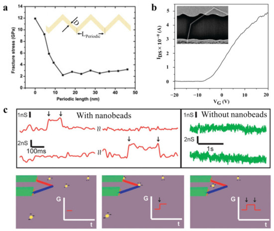
Figure 1.
Effects of nanowire kinking on different properties for mechanical (a), electronical (b), and biological (c) applications. (a) Fracture stress and fracture strain as a function of the periodic length L in zigzag kinked Si NWs alongside the nanowire schematic as the inset (adapted with permission from Ref. [3]. Copyright 2015 Elsevier). (b) Current−voltage data recorded from a FET built on a single kinked In2O3 nanowire. Inset: SEM image of the device structure. Scale bar is 2 μm (adapted with permission from Ref. [7]. Copyright 2011 American Chemical Society). (c) Nanobead sensing in kinked p–n nanowire devices. Top graphs show conductance vs. time data from two devices during nanobead introduction (left) and with only deionized water (right) in the microfluidic channel, marked by signal on/off points (black arrows). Bottom figures display schematic of the nanobead sensing process and the corresponding time-dependent conductance change in the device, with black arrows indicating signal on/off points. The blue and red lines designate the p-doped and n-doped arms, respectively (adapted with permission from Ref. [9]. Copyright 2012 American Chemical Society).
Nanowires can exhibit a single kink or multiple kinks, resulting in periodically modulated structures known as zigzags [12,13,14], sawtooth [15,16,17], or even wormy [18] shapes, as shown in Figure 2a–d. The emergence of kinks can be induced by adjusting growth conditions like vapor pressure, vapor composition, growth temperature, process time, seed composition, etc. The influence of these conditions on the fabrication of kinked nanowires and their potential impact on altering thermodynamical characteristics, together with their altered properties and potential innovative applications, have recently been thoroughly examined in a comprehensive review by Vlassov et al. [19].
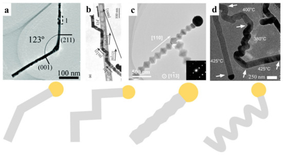
Figure 2.
TEM micrographs and schemes of various nanowire morphologies with single (a) or multiple kinks, including zigzag (b), sawtooth (c), and wormy (d) shapes. (a) Single kinked SnO2 nanowire (adapted with permission from Ref. [20]. Copyright 2015, The Royal Society of Chemistry). (b) Zigzag GaN nanowire (adapted with permission from Ref. [14]. Copyright 2005, AIP Publishing). (c) Sawtooth TiO2 nanowire (adapted with permission from Ref. [21]. Copyright 2019 WILEY-VCH Verlag GmbH & Co. KGaA, Weinheim). (d) Wormy-shaped Si nanowire (adapted with permission from Ref. [18]. Copyright 2009, American Chemical Society).
While these growth parameters are likely to have a high degree of coupling, the prediction of the occurrence of kinks during nanowire growth is further compounded. Since nucleation and lateral expansion of the growth species at the seed–nanowire interface are usually the pivotal stage in vapor-based growth, thermodynamic models [2] and kinetic models [22,23] have been well developed to describe the vapor growth of nanowires. The influencing parameters in these models are supersaturation in seeds, wetting angle at vapor–seed–nanowire interfaces, nanowire size, and surface/interface energies. Theoretical models for kinking will be briefly reviewed in Section 2. On a different note, an exploration of the microscopic attributes of nanowires, which entails an in-depth analysis of crystallographic orientations, defects, and stresses, can provide valuable insights while linking these microscopic attributes to the observed kinking behavior. Aligning with theoretical models, we reviewed the kinking behavior of nanowires as a consequence of different compositions in heterogeneous nanowires, the formation of stacking faults and twin planes in single-phase nanowires, and more interestingly, the local fluctuation induced in defect-free single-crystalline nanowires. Our objective is to forge a coherent connection between growth parameters and kinking behavior. This endeavor aspires to provide a predictive framework that enhances our understanding of kinking tendencies in nanowire growth.
2. Thermodynamic Considerations
Vapor–liquid–solid (VLS) growth was first reported in Si nanowires with Au seeds by Wagner and Ellis in 1964 [24]. VLS growth has several variants like vapor–solid–solid (VSS) growth [25,26], solid–liquid–solid (SLS) growth [27,28], and vapor–adsorption layer–solid (VAdS) growth [21,29]. The process comprises a sequence of four steps, including: (i) mass transport of growth species to the seed surface; (ii) absorption of growth species at the seed; (iii) diffusion of growth species inside the seed; and (iv) incorporation of growth species into nanowires, i.e., the nucleation and lateral expansion of the growth species at the seed/nanowire interface.
The rate-determining step is typically recognized as step (iv) [2]. By assessing the chemical potential of all species involved in this step, the change in free energy () can be evaluated using the following equation:
where is the length of the nanowires. The first term describes the driving force, where is the difference in chemical potential between the growth species within the seed and those of the nanowires, and is the cross-section of the nanowire.
The second term defines the contribution of the surface energy of the nanowire sidewall. is the nanowire perimeter. is the effective lateral surface energy of the nanowire. When a columnar nanowire is enclosed by different facets, refers to the contribution of individual facets, in which, and are the fraction and surface energy of facet . This simple model is employed to predict the switching of growth directions in different nanowires such Si [30], Ge [31,32], GaAs [33], and GeSn [34]. Figure 3 presents a diagram illustrating the configurations at the interfaces between the seed and nanowires, encompassing the parameters discussed earlier.
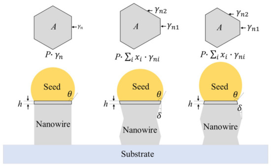
Figure 3.
Geometries at the seed–nanowire interface. and are the area and perimeter of grown nanowires with height h, respectively. is the contact angle. From left to right are cylindrical nanowires, nanowires with widening facets, and nanowires with narrowing facets. is the inclined angle for either widening facets or narrowing facets. and are the surface energy of the facets.
If facet has an incline angle with the nanowire growth direction (as shown in Figure 3, middle and right configurations), includes a correction factor considering the actual area of facet i per unit length [35]. The formation of inclined facets usually involves changes in the shape of seeds and the area of the seed–nanowire interface, the free energy change of which is defined as and , respectively. Although the precise formulations of and can become intricate, they are associated with the contact angle , incline angle , seed surface energy , and seed–nanowire interface energy . These relationships are usually derived with the assumptions that the seed retains a consistent volume during growth and the elementary volumes of the growth species are the same inside the seed and the nanowire [2]. If is much smaller than the radius of the seed, and can be simplified as the product of surface/interface energies and trigonometric functions of relevant angles, successfully predicting the sawtooth growth and its diameter-dependent spacing of Si [35], Ge [36], GaP [36], and TiO2 [17] nanowires. Furthermore, crystal defects, such as twin and stacking faults, are likely involved during the growth of the nanowire [37,38,39]. Correspondingly, the formation energy of these twins or stacking faults referred to as , which also contributes to the nanowire growth (). Incorporating the term, sawtooth patterns in GaAs [40] and InP [41] nanowires, as well as kinking in Ge nanowires [42], are well predicted.
In these cases where the rate-limiting process is the nucleation step, the above equation can be slightly modified to describe the nucleus at the seed–nanowire interface, i.e., the growth front. Variables , , and correspond to the area, perimeter, and effective surface/interface energy of the nucleus, respectively. Depending on the nucleation sites, at the triple phase line or in the center of the seed, the detailed formulation of these variables may differ. This conceptual framework has found utility in elucidating the sawtooth and kinking behaviors of various systems like Si [43], GaP [44], and InP [45].
As kinking involves the competition between two growth pathways, which likely have very close free energies, kinking is expected to be sensitive to slight changes in the free energy (). Any factors, such as changes in seed volume [46] changes in the surface energy of the nanowires due to surface decoration [18,47,48], and changes in seed–nanowire–vapor triple junctions [49,50], can prompt changes in the growth pathways. An integrated continuum model, which incorporates facet dynamics, seed statics, and the emergence of new facets, has been proposed by Schwarz and Tersoff [51]. This continuum model not only successfully captures the kinking behaviors, but also predicts distinct growth modes verified by in situ TEM observation of Au-catalyzed Si nanowire growth [52]. These models typically assume the seed–nanowire interface to be a sharp boundary, which is reasonable for most growth conditions characterized by low growth rates [53]. To address the influence of interface topology, especially the non-axisymmetric geometry of seeds on faceted nanowires, phase-field modeling [22,54] and MD simulations [55] are incorporated to successfully predict the formation of kinking [56], which is often associated with seed unpinning on non-axisymmetric seed–nanowire interfaces. When further examining the seed dynamics using a perturbation approach, Muaralidharan et al. [23] demonstrated that such non-axisymmetric unpinning transitions are inherently unstable, playing a key role in kinking formation. While minor variations in growth conditions can perturb individual parameters such as seeds and facet and seed surface energies, the direct connections between kinking behaviors and observed microstructures can also offer valuable insights. These connections are discussed in the following section.
3. Kinks in Heterostructure Nanowires
Nanowires processing heterostructures, characterized by distinct compositional/structural changes along their lengths, can exhibit preferential growth directions for individual segments and often deviate from their ideal growth trajectories, resulting in the emergence of their kinking morphology. Variations in surface energies among different segments and seed–nanowire interface energies, coupled with diverse surface energies exhibited by seeds of varying compositions, collectively contribute to the observed kinking behavior. Furthermore, lattice mismatches and discrepant thermal expansion coefficients between different structural domains can induce strain, impacting the overall stability [57]. The presence of abrupt compositional interfaces further influences the nucleation and growth processes at the growth front, helping in the development of kinks as the nanowire attempts to accommodate these structural disparities [58,59].
Kinking behaviors have been reported in group III-V and group IV heterostructure nanowires such as Si-GaP [46,60], GaP-InP [58], InAs-GaAs [58,61], InAs-InP [62], and GaAs-GaSb [63]. A few examples are shown in Figure 4a. This arises from the modifications of vapor compositions and corresponding changes in seed compositions. Paladugu et al. [61] detailed the growth of the InAs segment on GaAs by substituting trimethylgallium (TMG) for GaAs growth with trimethylindium (TMI) for InAs while maintaining AsH3 flow in a horizontal-flow metal–organic chemical vapor deposition (MOCVD) reactor. This led to changes in seed composition and subsequent displacement of seeds during the InAs growth period, attributed to lower Au/GaAs interfacial energy compared to that of Au/InAs. Zannier et al. [64] also linked kinking behavior to a low group III-to-Au ratio in the seeds stemming from seed instability and droplet wetting along the sidewalls. On the other hand, Dick et al. [58] reported the influence of growth sequences of segments on their kinking behaviors for various heterostructure nanowires grown using the MOCVD technique. For example, when the GaP segment is grown on Si, the nanowire remains straight; conversely, when the Si segment is grown on GaP, it exhibits kinking. Dick et al. [58] and Ross et al. [59] speculated that the emergence of kinks is linked to island growth (Volmer–Weber) occurring at the seed–nanowire interface rather than the energetically more favorable layer-by-layer growth (Frank-van der Merwe), which depends on the nanowire and seed composition. It is noteworthy that precisely controlling growth conditions, including temperature, vapor, and seed, can yield straight heterogeneous nanowires in various systems such as Si/Ge [65,66,67], Si/GaP [46,60], GaP-InP [58], etc.
Group III–V nanowires, having cubic symmetry zinc blende (ZB) structures, are predominantly grown along <100>ZB and are defect-free; however, ZB/WZ (Wurtzite, hexagonal symmetry) mixed structures are observed for most nanowires grown along the <111>ZB//<0001>WZ nanowires [25,68]. Such phase transitions can occur during nanowire growth [69], resulting in a kinking morphology, particularly when changing the growth temperature and atmosphere. Zhou et al. [70] demonstrated ZB/WZ phase translations in InAs and InP nanowires with a slight incorporation of Sb. Zhang et al. [71] reported this kinking phenomenon in InAs nanowires, from <0001>WZ segments to defect-free <001>ZB in Figure 4b. This is mainly achieved by manipulating the In content in the Au seed at different V/III vapor ratios, together with a small in-plane lattice mismatch at the seed–nanowire interface. Encountered at the junction of multiple titled ZB nanowires, WZ connection segments have been noted in various systems, such as InAs [72] and InSb [73]. Similarly intriguing hexagonal/cubic transitions have been discovered in Si nanowires. A hexagonal Si polymorph is reported by Morral et al. [74] within Si nanowires, and hexagonal Si segments have been observed by He et al. [75], corresponding to the kinking of Si nanowires.
In addition, the introduction of defects can play a crucial role in triggering the formation of kinks within distinct segments of nanowires, often correlating with localized lattice mismatches and stress disparities. Dayeh et al. [43] reported a 19.5° kinking in Au-catalyzed hybrid Ge−Si NWs, evident during higher Si growth rates. This is attributed to the formation of inclined twin boundaries. As a result, it drives nanowire diameter expansion and disturbs the line tension at the vapor, seed, and nanowire triple boundaries, thus switching the growth direction from ⟨111⟩ to ⟨211⟩, as shown in Figure 4c.

Figure 4.
Kinked nanowires induced by different phases: (a) with different compositions, (b) with the same composition, and (c) involving crystal defects (stacking faults and twinning). (a) (1–4) Microstructure of various heterostructure nanowires showing how the relative order of nanowire compositions stacked atop one another influences the formation of either a kink or a straight nanowire (adapted with permission from Ref. [58]. Copyright 2007 American Chemical Society). (b) TEM image of a kinked InAs nanowire illustrating a phase change from wurtzite <> to a zinc blend <> (Adapted with permission from Ref. [71]. Copyright 2015 American Chemical Society). (c) Kinked Ge-Si axial nanowire heterostructure induced by crystal defects. A HRTEM image alongside a molecular dynamics simulation demonstrates how the initiation of a twin boundary in the <112> direction results in a 19.5° kink (adapted with permission from Ref. [43]. Copyright 2011 American Chemical Society).

4. Kinking Associated with Stacking Faults and Twins
While planar defects like stacking faults and twins can be introduced into heterostructure nanowires, resulting in kinking behaviors, it is important to note that in many single-phase nanowires, like Si [76,77], Ge [42], GeSn [34], GaP [78], and ZnO [79], stacking faults and twins emerge as the dominant factors influencing kinking tendencies, as indicated by the term in Equation (1). These planar defects are either parallel to, inclined with respect to, or perpendicular to the growth direction of the nanowires. Within a single kinked nanowire, either a particular orientation type of planar defect or a combination of various orientation types can manifest, thereby giving rise to diverse kink angles. He et al. [39] reported that a multitude of twins and diverse twin types are present at kinks, corresponding to kink angles of ~71°, ~90°, ~109°, ~125°, ~130°, ~141°, and ~160° in In-catalyzed Si nanowires. These can grow in multiple growth directions, including <100>, <110>, <111>, <112>, and <113> under the given growth conditions, as shown in Figure 5a. Similarly, various combinations of differently oriented twins were observed at ~70° and ~110° kinks in Au-catalyzed InP nanowires with ZB structures by Zhang et al. [80] and at ~70°, ~110° and ~124° kinks in GaP nanowires with ZB structures by Krug et al. [78]. Using ZnO nanowires, Zhang et al. [79] discovered the presence of {} and {} twins and notable stacking faults at ~57°, ~70°, and ~117° kinks. Sb doping was adopted to trigger twinning and stabilize specific twin boundaries through Sb segregation.
How kinks are facilitated by inclined and parallel twins at the growth front has been discussed within various nanowire systems. Lenrick et al. [81] recorded a kinking process involving inclined twins in InAs nanowires, highlighting the pivotal role of the intersection between such inclined twins and the seed–nanowire interface. A second twin forms to accommodate this structural change, leading to shifts in growth directions. Koivusalo et al. [82] proposed a twin-mediated growth mode in self-catalyzed GaAs nanowires. This growth mode was attributed to the oscillation of the seed–nanowire interface between the two distinct flat (111) facets with differing polarities. Impressively, they achieved a remarkable 100% yield in altering the growth direction from vertical to horizontal through systematically optimizing the growth conditions, as illustrated in Figure 5b. Such seed–nanowire interface oscillation in InP nanowires has also been recorded using the in situ TEM technique [78].
Stacking faults and twins oriented perpendicular to the growth direction has been frequently observed in <111>ZB-grown group III–V nanowires. These can merge both as the ZB/WZ interfaces and within pure ZB structure, marked by coherent twins. The ZB segments are enclosed by {111} sidewalls, thus resulting in a distinct kink angle of ~141°. Particularly, a periodic twinned structure has been promoted through the addition of zinc in vapor during growth, as demonstrated in InP [41] and GaP [83] nanowires by Algra et al. as well as GaAs nanowires by Burgess et al. [40]. Caroff et al. [84] synthesized periodic twinned InAs nanowires across a wide range of diameters at high growth temperatures. A similar phenomenon has been observed in <0001>-grown wurtzite ZnO nanowires, particularly when doped with Sn [85], and in <111>-grown Zn2SnO4 nanowires at optimized growth temperatures [86], as shown in Figure 5c. The underlying mechanism involves distortion of the seed in response to the evolution of the cross-sectional shape of the nanowires while switching twin segments. In alignment with this mechanism, the spacing between twin segments exhibits a diameter-dependent behavior; a prediction that has been substantiated in various reported nanowire instances.

Figure 5.
Kinked nanowires induced by twins/stacking faults in single-phase nanowires. (a) Microstructure of different kinking in In-catalyzed Si nanowires caused by a combination of the three types of twins (adapted with permission from Ref. [39]. Copyright 2015, The Royal Society of Chemistry). (b) GaAs Nanowire kinking caused by a single twin plane present in the horizontal section. Two different droplet–NW interfaces are dominated by a flat (111)B plane in part 3 and (111)A plane in part 4. (adapted with permission from Ref. [82]. Copyright 2019, American Chemical Society). (c) (1) TEM image of a periodic twin superlattice in Zn2SnO4 (ZTO) nanowires creating a sawtooth shape (1) alongside a schematic of the twin planes labelled by red lines (2) (adapted from Ref. [86]. Copyright 2008 American Chemical Society).

5. Kinking in Defect-Free Single-Crystal Nanowires
Kinking in defect-free single-crystal nanowires is often ascribed to the dynamic interplay between intrinsic material anisotropy and growth dynamics. As nanowires grow, a fresh balance between crystallographic orientations and surface energy gradients can develop, consequently resulting in localized deviations from the initially straight growth trajectory. Under identical growth conditions, kinked nanowires can coexist with their straight counterparts featuring homogenous seeds, which can be attributed to size-dependent free energy that varies across different oriented nanowires. This behavior has been observed across diverse nanowire systems, including Si [87], Ge [31], and In2O3 [88]. Kinking frequently occurs under growth conditions that can favor multiple growth directions, as reported in ZnO [18] and SnO2 [89].
The controlled synthesis of kinked nanowires can be achieved through strategic alterations in global growth conditions like temperature and vapor, or by inducing localized perturbations within growth conditions that may accommodate multiple growth directions. Tian et al. [6], for instance, showcased the feasibility of creating connection segments while momentarily purging vapor reactant between two straight <112>-oriented segments produced under supersaturated reactants. Its success has been demonstrated in producing 120° kinks in Si, Ge, and GdS. Conversely, Musin et al. [32] introduced methyl germane (GeH3CH3) instead of germane (GeH4) vapor, enabling the growth of both <110>- and <111>-oriented nanowires at identical growth temperatures. This manipulation allowed for the formation of multiple kink angles, creating connections between <110>- and <111>-oriented Ge segments, as shown in Figure 6a.
An additional mechanism of vapor-induced kinks revolves around the passivation of nanowire surfaces, effectively reducing surface energies ( in Equation (1)) and thereby stabilizing new facets. During Au-seeded nanowire growth, the attachment of Au adatoms or clusters to the nanowire surface can be involved, consequently altering the kink behaviors of Si nanowires, as reported by Madras et al. [18]. Shin and Filler [90] produced kinked nanowires through the addition of hydrogen to Si nanowire sidewalls. The authors demonstrated that surface chemistry, i.e., covalently bonded hydrogen atoms, is responsible for the commonly observed transition in Si nanowires from ⟨111⟩ to ⟨112⟩ in their growth direction.
The controllable synthesis of kinks can also be facilitated by enhancing localized perturbations during growth, such as varying seed compositions and structural fluctuations in inhomogeneous seeds. For instance, Ge nanowires exhibited a <111> to <110> kink due to Ga diffusion into the Au seed at high temperatures [91]. The growth trajectory of GaN nanowires with an Au–Ni bimetallic seed can shift from <> for Ni-rich seeds to <> for Au-rich seed while remaining a single-crystal structure, as shown in Figure 6b. The underlying mechanism involves Ni incorporation into either the nanowire’s bulk or its surface sites, along with the formation of volatile Ni-containing species [92]. On the other hand, kinked TiO2 nanowires from <110> to <111> are observed using Au–Ag bimetallic seeds. This kinking arose due to an unexpected Ag-rich segregation at the growth front, altering the force balance at the triple phase line (represented by , , and , resulting in corresponding changes in and in Equation (1)), as illustrated in Figure 6c. This segregation can also influence the adsorption and mass transfer behaviors of growth species, consequently influencing the nucleation sites and changing the growth direction without introducing defects [21,93].

Figure 6.
Kinking in a single-crystalline nanowire. (a) Effect of vapor species modulation on kinking: Ge nanowire kinking superstructures are created at 325 °C by controlling GeH3CH3 injection during VLS growth. SEM images show various superstructures with distinct GeH3CH3 cycling times (adapted with permission from Ref. [32]. Copyright 2012 American Chemical Society). (b) Effect of seed composition on kinking: TEM images and CBED diffraction pattern of GaN nanowire with an Au–Ni bimetallic seed illustrating growth direction switching (adapted with permission from Ref. [92]. Copyright 2014 American Chemical Society). (c) Effect of structural fluctuation of inhomogeneous seeds on kinking: SEM image show kinked TiO2 nanowire with an Au–Ag bimetallic seed (scale bar is 1 µm). TEM image alongside the 3D model indicates the growth direction change from <110> to <111> (scale bar is 500 nm). EDX elemental mapping of a bead-shaped nanowire (top) and a prismatic nanowire (bottom) with scale bars of 50 nm. They both demonstrate the segregation of Ag, which is located at the nanowire–seed interface for kinked nanowires (Adapted with permission from Ref. [21]. Copyright 2019 WILEY-VCH Verlag GmbH & Co. KGaA, Weinheim).

6. Conclusions and Outlook
Kinking, a phenomenon characterized by abrupt changes in the growth direction of vapor-based nanowires, has emerged as a compelling avenue of exploration in recent years. This phenomenon has evolved into a powerful tool for tailoring the morphology and properties of nanowires. Various studies have highlighted the multifaceted nature of factors influencing the growth direction, including temperature, vapor pressure, precursor composition, substrate treatment, catalyst size, and more. These factors are interconnected, complicating the precise control of nanowire morphology. Theoretically, the interplay between intrinsic material anisotropy, such as the surface energy, inclined angle of enclosed facets, and growth dynamics, e.g., nucleation and lateral expansion processes, governs the growth direction of nanowires. Despite comprehensive models which have been developed to incorporate these factors, many factors are difficult to quantify experimentally and can be easily altered by even minor fluctuations in growth conditions. This limits the capabilities of these models to predict kinking formation.
Kinking behaviors exhibit distinct pathways in homostructure and heterostructure nanowires. In heterostructure nanowires, diverse compositions and crystal structures in individual segments, as well as crystal defects, can lead to kinking. Conversely, stacking faults and twins likely dominate the kinking behaviors of homostructure nanowires. The orientation of stacking faults and twins, whether parallel, perpendicular, or inclined, crucially alters the subsequent growth direction of nanowires. Remarkably, a few defect-free single-crystal nanowires have been reported with kinking behaviors through precise control of their vapor and seed compositions, validating the key factor in theoretical models and unlocking avenues for fabricating kinked nanowires in a controlled manner.
While advances have been made, there remains a compelling need for unveiling the intricate mechanisms governing growth directions, particularly in defect-free homostructure single-crystalline nanowires. Moreover, the potential applications of kinked nanowires, particularly as nanoelectronics and biosensors, have gained traction, which can be further developed by gaining effective control over the nanowire morphology.
Author Contributions
This manuscript has been written by Z.R. and G.Z. All authors have read and agreed to the published version of the manuscript.
Funding
We gratefully acknowledge the financial support of the University of Manitoba and Canada Research Chair program.
Conflicts of Interest
The authors declare no conflict of interest.
References
- Wacaser, B.A.; Dick, K.A.; Johansson, J.; Borgström, M.T.; Deppert, K.; Samuelson, L. Preferential Interface Nucleation: An Expansion of the VLS Growth Mechanism for Nanowires. Adv. Mater. 2009, 21, 153–165. [Google Scholar] [CrossRef]
- Dubrovskii, V.G. Nucleation Theory and Growth of Nanostructures; NanoScience and Technology; Springer: Berlin/Heidelberg, Germany, 2014. [Google Scholar]
- Jing, Y.; Zhang, C.; Liu, Y.; Guo, L.; Meng, Q. Mechanical Properties of Kinked Silicon Nanowires. Phys. B Condens. Matter 2015, 462, 59–63. [Google Scholar] [CrossRef]
- Chen, Y.; Zhang, C.; Li, L.; Tuan, C.-C.; Chen, X.; Gao, J.; He, Y.; Wong, C.-P. Effects of Defects on the Mechanical Properties of Kinked Silicon Nanowires. Nanoscale Res. Lett. 2017, 12, 185. [Google Scholar] [CrossRef] [PubMed]
- Jiang, J.-W.; Zhao, J.-H.; Rabczuk, T. Size-Sensitive Young’s Modulus of Kinked Silicon Nanowires. Nanotechnology 2013, 24, 185702. [Google Scholar] [CrossRef] [PubMed][Green Version]
- Tian, B.; Xie, P.; Kempa, T.J.; Bell, D.C.; Lieber, C.M. Single-Crystalline Kinked Semiconductor Nanowire Superstructures. Nat. Nanotechnol. 2009, 4, 824–829. [Google Scholar] [CrossRef] [PubMed]
- Shen, G.; Liang, B.; Wang, X.; Chen, P.-C.; Zhou, C. Indium Oxide Nanospirals Made of Kinked Nanowires. ACS Nano 2011, 5, 2155–2161. [Google Scholar] [CrossRef] [PubMed]
- Cook, B.G.; Varga, K. Conductance of Kinked Nanowires. Appl. Phys. Lett. 2011, 98, 052104. [Google Scholar] [CrossRef]
- Jiang, Z.; Qing, Q.; Xie, P.; Gao, R.; Lieber, C.M. Kinked P-n Junction Nanowire Probes for High Spatial Resolution Sensing and Intracellular Recording. Nano Lett. 2012, 12, 1711–1716. [Google Scholar] [CrossRef]
- Tian, B.; Cohen-Karni, T.; Qing, Q.; Duan, X.; Xie, P.; Lieber, C.M. Three-Dimensional, Flexible Nanoscale Field-Effect Transistors as Localized Bioprobes. Science 2010, 329, 830–834. [Google Scholar] [CrossRef]
- Xu, L.; Jiang, Z.; Qing, Q.; Mai, L.; Zhang, Q.; Lieber, C.M. Design and Synthesis of Diverse Functional Kinked Nanowire Structures for Nanoelectronic Bioprobes. Nano Lett. 2013, 13, 746–751. [Google Scholar] [CrossRef]
- Peng, H.; Meister, S.; Chan, C.K.; Zhang, X.F.; Cui, Y. Morphology Control of Layer-Structured Gallium Selenide Nanowires. Nano Lett. 2007, 7, 199–203. [Google Scholar] [CrossRef]
- Hughes, W.L.; Wang, Z.L. Formation of Piezoelectric Single-Crystal Nanorings and Nanobows. J. Am. Chem. Soc. 2004, 126, 6703–6709. [Google Scholar] [CrossRef] [PubMed]
- Zhou, X.T.; Sham, T.K.; Shan, Y.Y.; Duan, X.F.; Lee, S.T.; Rosenberg, R.A. One-Dimensional Zigzag Gallium Nitride Nanostructures. J. Appl. Phys. 2005, 97, 104315. [Google Scholar] [CrossRef]
- Panda, S.; Datta, A.; Sinha, G.; Chaudhuri, S. Synthesis of Well-Crystalline GaS Nanobelts and Their Unique Field Emission Behavior. J. Phys. Chem. C 2008, 112, 6240–6244. [Google Scholar] [CrossRef]
- Hong, W.-K.; Sohn, J.I.; Hwang, D.-K.; Kwon, S.-S.; Jo, G.; Song, S.; Kim, S.-M.; Ko, H.-J.; Park, S.-J.; Welland, M.E.; et al. Tunable Electronic Transport Characteristics of Surface-Architecture-Controlled ZnO Nanowire Field Effect Transistors. Nano Lett. 2008, 8, 950–956. [Google Scholar] [CrossRef]
- Zhou, P.; Liu, Y.; Zhu, G. Sawtooth Faceting in Rutile Nanowires. ACS Omega 2022, 7, 10406–10412. [Google Scholar] [CrossRef] [PubMed]
- Madras, P.; Dailey, E.; Drucker, J. Kinetically Induced Kinking of Vapor−Liquid−Solid Grown Epitaxial Si Nanowires. Nano Lett. 2009, 9, 3826–3830. [Google Scholar] [CrossRef]
- Vlassov, S.; Oras, S.; Polyakov, B.; Butanovs, E.; Kyritsakis, A.; Zadin, V. Kinking in Semiconductor Nanowires: A Review. Cryst. Growth Des. 2022, 22, 871–892. [Google Scholar] [CrossRef]
- Gan, L.; Liao, M.; Li, H.; Ma, Y.; Zhai, T. Geometry-Induced High Performance Ultraviolet Photodetectors in Kinked SnO2 Nanowires. J. Mater. Chem. C 2015, 3, 8300–8306. [Google Scholar] [CrossRef]
- Xie, D.Y.; Lin, M.; Zhou, W.; Wang, J.; Zhu, G. Kinetically Favorable Vapor–Adsorbate–Solid Growth of Rutile Nanowires. Small Methods 2019, 3, 1900111. [Google Scholar] [CrossRef]
- Schwalbach, E.J.; Davis, S.H.; Voorhees, P.W.; Wheeler, D.; Warren, J.A. Liquid Droplet Dynamics and Complex Morphologies in Vapor–Liquid–Solid Nanowire Growth. J. Mater. Res. 2011, 26, 2186–2198. [Google Scholar] [CrossRef]
- Muralidharan, S.; Voorhees, P.W.; Davis, S.H. Nonaxisymmetric Droplet Unpinning in Vapor-Liquid-Solid-Grown Nanowires. J. Appl. Phys. 2013, 114, 114305. [Google Scholar] [CrossRef]
- Wagner, R.S.; Ellis, W.C. Vapor-liquid-solid Mechanism of Single Crystal Growth. Appl. Phys. Lett. 1964, 4, 89–90. [Google Scholar] [CrossRef]
- Kamins, T.I.; Stanley Williams, R.; Basile, D.P.; Hesjedal, T.; Harris, J.S. Ti-Catalyzed Si Nanowires by Chemical Vapor Deposition: Microscopy and Growth Mechanisms. J. Appl. Phys. 2001, 89, 1008–1016. [Google Scholar] [CrossRef]
- Persson, A.I.; Larsson, M.W.; Stenström, S.; Ohlsson, B.J.; Samuelson, L.; Wallenberg, L.R. Solid-Phase Diffusion Mechanism for GaAs Nanowire Growth. Nat. Mater. 2004, 3, 677–681. [Google Scholar] [CrossRef] [PubMed]
- Yan, H.F.; Xing, Y.J.; Hang, Q.L.; Yu, D.P.; Wang, Y.P.; Xu, J.; Xi, Z.H.; Feng, S.Q. Growth of Amorphous Silicon Nanowires via a Solid–Liquid–Solid Mechanism. Chem. Phys. Lett. 2000, 323, 224–228. [Google Scholar] [CrossRef]
- Yang, Q.; Lu, Z.; Liu, J.; Lei, X.; Chang, Z.; Luo, L.; Sun, X. Metal Oxide and Hydroxide Nanoarrays: Hydrothermal Synthesis and Applications as Supercapacitors and Nanocatalysts. Prog. Nat. Sci. Mater. Int. 2013, 23, 351–366. [Google Scholar] [CrossRef]
- Bootsma, G.A.; Gassen, H.J. A Quantitative Study on the Growth of Silicon Whiskers from Silane and Germanium Whiskers from Germane. J. Cryst. Growth 1971, 10, 223–234. [Google Scholar] [CrossRef]
- Schwarz, K.W.; Tersoff, J.; Kodambaka, S.; Chou, Y.-C.; Ross, F.M. Geometrical Frustration in Nanowire Growth. Phys. Rev. Lett. 2011, 107, 265502. [Google Scholar] [CrossRef]
- Li, Y.; Wang, Y.; Ryu, S.; Marshall, A.F.; Cai, W.; McIntyre, P.C. Spontaneous, Defect-Free Kinking via Capillary Instability during Vapor–Liquid–Solid Nanowire Growth. Nano Lett. 2016, 16, 1713–1718. [Google Scholar] [CrossRef]
- Musin, I.R.; Filler, M.A. Chemical Control of Semiconductor Nanowire Kinking and Superstructure. Nano Lett. 2012, 12, 3363–3368. [Google Scholar] [CrossRef] [PubMed]
- Wu, Z.H.; Mei, X.; Kim, D.; Blumin, M.; Ruda, H.E.; Liu, J.Q.; Kavanagh, K.L. Growth, Branching, and Kinking of Molecular-Beam Epitaxial ⟨110⟩ GaAs Nanowires. Appl. Phys. Lett. 2003, 83, 3368–3370. [Google Scholar] [CrossRef]
- Sun, Y.-L.; Matsumura, R.; Jevasuwan, W.; Fukata, N. Au–Sn Catalyzed Growth of Ge1−xSnx Nanowires: Growth Direction, Crystallinity, and Sn Incorporation. Nano Lett. 2019, 19, 6270–6277. [Google Scholar] [CrossRef] [PubMed]
- Ross, F.M.; Tersoff, J.; Reuter, M.C. Sawtooth Faceting in Silicon Nanowires. Phys. Rev. Lett. 2005, 95, 146104. [Google Scholar] [CrossRef] [PubMed]
- Wen, C.-Y.; Tersoff, J.; Hillerich, K.; Reuter, M.C.; Park, J.H.; Kodambaka, S.; Stach, E.A.; Ross, F.M. Periodically Changing Morphology of the Growth Interface in Si, Ge, and GaP Nanowires. Phys. Rev. Lett. 2011, 107, 025503. [Google Scholar] [CrossRef] [PubMed]
- Lin, M.; Liu, Y.; Zhu, G. Mn-Promoted Growth of Mg-Based Spinel and Pyroxene Nanostructures. ACS Omega 2020, 5, 1566–1571. [Google Scholar] [CrossRef] [PubMed]
- Wu, S.; Wu, S.; Song, W.; Wang, L.; Yi, X.; Liu, Z.; Wang, J.; Li, J. Crystal Phase Evolution in Kinked GaN Nanowires. Nanotechnology 2020, 31, 145713. [Google Scholar] [CrossRef]
- He, Z.; Nguyen, H.T.; Toan, L.D.; Pribat, D. A Detailed Study of Kinking in Indium-Catalyzed Silicon Nanowires. CrystEngComm 2015, 17, 6286–6296. [Google Scholar] [CrossRef]
- Burgess, T.; Breuer, S.; Caroff, P.; Wong-Leung, J.; Gao, Q.; Hoe Tan, H.; Jagadish, C. Twinning Superlattice Formation in GaAs Nanowires. ACS Nano 2013, 7, 8105–8114. [Google Scholar] [CrossRef]
- Algra, R.E.; Verheijen, M.A.; Borgström, M.T.; Feiner, L.-F.; Immink, G.; van Enckevort, W.J.P.; Vlieg, E.; Bakkers, E.P.A.M. Twinning Superlattices in Indium Phosphide Nanowires. Nature 2008, 456, 369–372. [Google Scholar] [CrossRef]
- Geaney, H.; Dickinson, C.; Weng, W.; Kiely, C.J.; Barrett, C.A.; Gunning, R.D.; Ryan, K.M. Role of Defects and Growth Directions in the Formation of Periodically Twinned and Kinked Unseeded Germanium Nanowires. Cryst. Growth Des. 2011, 11, 3266–3272. [Google Scholar] [CrossRef]
- Dayeh, S.A.; Wang, J.; Li, N.; Huang, J.Y.; Gin, A.V.; Picraux, S.T. Growth, Defect Formation, and Morphology Control of Germanium–Silicon Semiconductor Nanowire Heterostructures. Nano Lett. 2011, 11, 4200–4206. [Google Scholar] [CrossRef] [PubMed]
- Johansson, J.; Karlsson, L.S.; Patrik, T.; Svensson, C.; Mårtensson, T.; Wacaser, B.A.; Deppert, K.; Samuelson, L.; Seifert, W. Structural Properties of ⟨111⟩B -Oriented III–V Nanowires. Nat. Mater. 2006, 5, 574–580. [Google Scholar] [CrossRef] [PubMed]
- Wang, J.; Plissard, S.R.; Verheijen, M.A.; Feiner, L.-F.; Cavalli, A.; Bakkers, E.P.A.M. Reversible Switching of InP Nanowire Growth Direction by Catalyst Engineering. Nano Lett. 2013, 13, 3802–3806. [Google Scholar] [CrossRef]
- Hillerich, K.; Dick, K.; Wen, C.-Y.; Reuter, M.; Kodambaka, S.; Ross, F. Strategies to Control Morphology in Hybrid Group III–V/Group IV Heterostructure Nanowires. Nano Lett. 2013, 13, 903–908. [Google Scholar] [CrossRef] [PubMed]
- Hannon, J.B.; Kodambaka, S.; Ross, F.M.; Tromp, R.M. The Influence of the Surface Migration of Gold on the Growth of Silicon Nanowires. Nature 2006, 440, 69–71. [Google Scholar] [CrossRef] [PubMed]
- Li, F.; Nellist, P.; Cockayne, D. Doping-Dependent Nanofaceting on Silicon Nanowire Surfaces. Appl. Phys. Lett. 2009, 94, 263111. [Google Scholar] [CrossRef]
- Ma, Z.; McDowell, D.; Panaitescu, E.; Davydov, A.V.; Upmanyu, M.; Menon, L. Vapor–Liquid–Solid Growth of Serrated GaN Nanowires: Shape Selection Driven by Kinetic Frustration. J. Mater. Chem. C 2013, 1, 7294–7302. [Google Scholar] [CrossRef][Green Version]
- Davidson, F.M.; Lee, D.C.; Fanfair, D.D.; Korgel, B.A. Lamellar Twinning in Semiconductor Nanowires. J. Phys. Chem. C 2007, 111, 2929–2935. [Google Scholar] [CrossRef]
- Schwarz, K.W.; Tersoff, J. From Droplets to Nanowires: Dynamics of Vapor-Liquid-Solid Growth. Phys. Rev. Lett. 2009, 102, 206101. [Google Scholar] [CrossRef]
- Schwarz, K.W.; Tersoff, J.; Kodambaka, S.; Ross, F.M. Jumping-Catalyst Dynamics in Nanowire Growth. Phys. Rev. Lett. 2014, 113, 055501. [Google Scholar] [CrossRef] [PubMed]
- Roper, S.M.; Davis, S.H.; Norris, S.A.; Golovin, A.A.; Voorhees, P.W.; Weiss, M. Steady Growth of Nanowires via the Vapor-Liquid-Solid Method. J. Appl. Phys. 2007, 102, 034304. [Google Scholar] [CrossRef]
- Wang, N.; Upmanyu, M.; Karma, A. Phase-Field Model of Vapor-Liquid-Solid Nanowire Growth. Phys. Rev. Mater. 2018, 2, 033402. [Google Scholar] [CrossRef]
- Frolov, T.; Carter, W.C.; Asta, M. Capillary Instability in Nanowire Geometries. Nano Lett. 2014, 14, 3577–3581. [Google Scholar] [CrossRef] [PubMed][Green Version]
- Roper, S.M.; Anderson, A.M.; Davis, S.H.; Voorhees, P.W. Radius Selection and Droplet Unpinning in Vapor-Liquid-Solid-Grown Nanowires. J. Appl. Phys. 2010, 107, 114320. [Google Scholar] [CrossRef]
- Ertekin, E.; Greaney, P.A.; Chrzan, D.C.; Sands, T.D. Equilibrium Limits of Coherency in Strained Nanowire Heterostructures. J. Appl. Phys. 2005, 97, 114325. [Google Scholar] [CrossRef]
- Dick, K.A.; Kodambaka, S.; Reuter, M.C.; Deppert, K.; Samuelson, L.; Seifert, W.; Wallenberg, L.R.; Ross, F.M. The Morphology of Axial and Branched Nanowire Heterostructures. Nano Lett. 2007, 7, 1817–1822. [Google Scholar] [CrossRef] [PubMed]
- Ross, F.M. Controlling Nanowire Structures through Real Time Growth Studies. Rep. Prog. Phys. 2010, 73, 114501. [Google Scholar] [CrossRef]
- Hocevar, M.; Immink, G.; Verheijen, M.; Akopian, N.; Zwiller, V.; Kouwenhoven, L.; Bakkers, E. Growth and Optical Properties of Axial Hybrid III–V/Silicon Nanowires. Nat. Commun. 2012, 3, 1266. [Google Scholar] [CrossRef]
- Paladugu, M.; Zou, J.; Guo, Y.-N.; Auchterlonie, G.J.; Joyce, H.J.; Gao, Q.; Hoe Tan, H.; Jagadish, C.; Kim, Y. Novel Growth Phenomena Observed in Axial InAs/GaAs Nanowire Heterostructures. Small 2007, 3, 1873–1877. [Google Scholar] [CrossRef]
- Svensson, S.F.; Jeppesen, S.; Thelander, C.; Samuelson, L.; Linke, H.; Dick, K.A. Control and Understanding of Kink Formation in InAs–InP Heterostructure Nanowires. Nanotechnology 2013, 24, 345601. [Google Scholar] [CrossRef] [PubMed]
- Kang, Y.; Hou, X.; Tang, J.; Chu, X.; Li, K.; Lin, F.; Jia, H.; Wang, X.; Wei, Z. Synthesis and Characterization of Kinked GaAs Nanowires by Sb Surfactant. Vacuum 2022, 196, 110778. [Google Scholar] [CrossRef]
- Zannier, V.; Ercolani, D.; Gomes, U.P.; David, J.; Gemmi, M.; Dubrovskii, V.G.; Sorba, L. Catalyst Composition Tuning: The Key for the Growth of Straight Axial Nanowire Heterostructures with Group III Interchange. Nano Lett. 2016, 16, 7183–7190. [Google Scholar] [CrossRef] [PubMed]
- Wen, C.-Y.; Reuter, M.C.; Bruley, J.; Tersoff, J.; Kodambaka, S.; Stach, E.A.; Ross, F.M. Formation of Compositionally Abrupt Axial Heterojunctions in Silicon-Germanium Nanowires. Science 2009, 326, 1247–1250. [Google Scholar] [CrossRef] [PubMed]
- Gamalski, A.D.; Perea, D.E.; Yoo, J.; Li, N.; Olszta, M.J.; Colby, R.; Schreiber, D.K.; Ducati, C.; Picraux, S.T.; Hofmann, S. Catalyst Composition and Impurity-Dependent Kinetics of Nanowire Heteroepitaxy. ACS Nano 2013, 7, 7689–7697. [Google Scholar] [CrossRef] [PubMed]
- Geaney, H.; Mullane, E.; Ramasse, Q.M.; Ryan, K.M. Atomically Abrupt Silicon-Germanium Axial Heterostructure Nanowires Synthesized in a Solvent Vapor Growth System. Nano Lett. 2013, 13, 1675–1680. [Google Scholar] [CrossRef] [PubMed]
- Fortuna, S.A.; Li, X. Metal-Catalyzed Semiconductor Nanowires: A Review on the Control of Growth Directions. Semicond. Sci. Technol. 2010, 25, 024005. [Google Scholar] [CrossRef]
- Glas, F.; Harmand, J.-C.; Patriarche, G. Why Does Wurtzite Form in Nanowires of III-V Zinc Blende Semiconductors? Phys. Rev. Lett. 2007, 99, 146101. [Google Scholar] [CrossRef]
- Zhou, H.; Pozuelo, M.; Hicks, R.; Kodambaka, S. Self-Catalyzed Vapor-Liquid-Solid Growth of InP1−XSbX Nanostructures. J. Cryst. Growth 2011, 319, 25–30. [Google Scholar] [CrossRef]
- Zhang, Z.; Zheng, K.; Lu, Z.-Y.; Chen, P.-P.; Lu, W.; Zou, J. Catalyst Orientation-Induced Growth of Defect-Free Zinc-Blende Structured ⟨00⟩ InAs Nanowires. Nano Lett. 2015, 15, 876–882. [Google Scholar] [CrossRef]
- Krizek, F.; Kanne, T.; Razmadze, D.; Johnson, E.; Nygård, J.; Marcus, C.M.; Krogstrup, P. Growth of InAs Wurtzite Nanocrosses from Hexagonal and Cubic Basis. Nano Lett. 2017, 17, 6090–6096. [Google Scholar] [CrossRef]
- Car, D.; Wang, J.; Verheijen, M.A.; Bakkers, E.P.A.M.; Plissard, S.R. Rationally Designed Single-Crystalline Nanowire Networks. Adv. Mater. 2014, 26, 4875–4879. [Google Scholar] [CrossRef] [PubMed]
- Fontcuberta i Morral, A.; Arbiol, J.; Prades, J.D.; Cirera, A.; Morante, J.R. Synthesis of Silicon Nanowires with Wurtzite Crystalline Structure by Using Standard Chemical Vapor Deposition. Adv. Mater. 2007, 19, 1347–1351. [Google Scholar] [CrossRef]
- He, Z.; Maurice, J.-L.; Li, Q.; Pribat, D. Direct Evidence of 2H Hexagonal Si in Si Nanowires. Nanoscale 2019, 11, 4846–4853. [Google Scholar] [CrossRef]
- Kim, J.H.; Moon, S.R.; Kim, Y.; Chen, Z.G.; Zou, J.; Choi, D.Y.; Joyce, H.J.; Gao, Q.; Tan, H.H.; Jagadish, C. Taper-Free and Kinked Germanium Nanowires Grown on Silicon via Purging and the Two-Temperature Process. Nanotechnology 2012, 23, 115603. [Google Scholar] [CrossRef]
- Potts, H.; Morgan, N.P.; Tütüncüoglu, G.; Friedl, M.; Morral, A.F.i. Tuning Growth Direction of Catalyst-Free InAs(Sb) Nanowires with Indium Droplets. Nanotechnology 2016, 28, 054001. [Google Scholar] [CrossRef]
- Krug, D.; Widemann, M.; Gruber, F.; Ahmed, S.; Demuth, T.; Beyer, A.; Volz, K. Kinking of GaP Nanowires Grown in an In Situ (S)TEM Gas Cell Holder. Adv. Mater. Interfaces 2023, 10, 2202507. [Google Scholar] [CrossRef]
- Li, S.; Zhang, X.; Zhang, L.; Gao, M. Twinning-Induced Kinking of Sb-Doped ZnO Nanowires. Nanotechnology 2010, 21, 435602. [Google Scholar] [CrossRef]
- Zhang, M.; Wang, F.; Wang, C.; Wang, Y.; Yip, S.; Ho, J.C. Formation Mechanisms for the Dominant Kinks with Different Angles in InP Nanowires. Nanoscale Res. Lett. 2014, 9, 211. [Google Scholar] [CrossRef]
- Lenrick, F.; Ek, M.; Deppert, K.; Samuelson, L.; Reine Wallenberg, L. Straight and Kinked InAs Nanowire Growth Observed in Situ by Transmission Electron Microscopy. Nano Res. 2014, 7, 1188–1194. [Google Scholar] [CrossRef]
- Koivusalo, E.S.; Hakkarainen, T.V.; Galeti, H.V.A.; Gobato, Y.G.; Dubrovskii, V.G.; Guina, M.D. Deterministic Switching of the Growth Direction of Self-Catalyzed GaAs Nanowires. Nano Lett. 2019, 19, 82–89. [Google Scholar] [CrossRef] [PubMed]
- Algra, R.E.; Hocevar, M.; Verheijen, M.A.; Zardo, I.; Immink, G.G.W.; van Enckevort, W.J.P.; Abstreiter, G.; Kouwenhoven, L.P.; Vlieg, E.; Bakkers, E.P.A.M. Crystal Structure Transfer in Core/Shell Nanowires. Nano Lett. 2011, 11, 1690–1694. [Google Scholar] [CrossRef] [PubMed]
- Caroff, P.; Dick, K.A.; Johansson, J.; Messing, M.E.; Deppert, K.; Samuelson, L. Controlled Polytypic and Twin-Plane Superlattices in III–V Nanowires. Nat. Nanotechnol. 2009, 4, 50–55. [Google Scholar] [CrossRef] [PubMed]
- Kim, S.; Na, S.; Jeon, H.; Kim, S.; Lee, B.; Yang, J.; Kim, H.; Lee, H.-J. Effects of Sn Doping on the Growth Morphology and Electrical Properties of ZnO Nanowires. Nanotechnology 2013, 24, 065703. [Google Scholar] [CrossRef] [PubMed]
- Wang, J.; Sun, X.W.; Xie, S.; Zhou, W.; Yang, Y. Single-Crystal and Twinned Zn2SnO4 Nanowires with Axial Periodical Structures. Cryst. Growth Des. 2008, 8, 707–710. [Google Scholar] [CrossRef]
- Schmidt, V.; Senz, S.; Gösele, U. Diameter-Dependent Growth Direction of Epitaxial Silicon Nanowires. Nano Lett. 2005, 5, 931–935. [Google Scholar] [CrossRef] [PubMed]
- Shen, Y.; Lebedev, O.I.; Turner, S.; Van Tendeloo, G.; Song, X.; Yu, X.; Wang, Q.; Chen, H.; Dayeh, S.A.; Wu, T. Size-Induced Switching of Nanowire Growth Direction: A New Approach Toward Kinked Nanostructures. Adv. Funct. Mater. 2016, 26, 3687–3695. [Google Scholar] [CrossRef]
- Kar, A.; Stroscio, M.A.; Dutta, M.; Meyyappan, M. Electronic Properties of Y-Junctions in SnO2 Nanowires. Phys. Status Solidi B 2011, 248, 2848–2852. [Google Scholar] [CrossRef]
- Shin, N.; Filler, M.A. Controlling Silicon Nanowire Growth Direction via Surface Chemistry. Nano Lett. 2012, 12, 2865–2870. [Google Scholar] [CrossRef]
- Song, M.S.; Jung, J.H.; Kim, Y.; Wang, Y.; Zou, J.; Joyce, H.J.; Gao, Q.; Tan, H.H.; Jagadish, C. Vertically Standing Ge Nanowires on GaAs(110) Substrates. Nanotechnology 2008, 19, 125602. [Google Scholar] [CrossRef][Green Version]
- Kuykendall, T.R.; Altoe, M.V.P.; Ogletree, D.F.; Aloni, S. Catalyst-Directed Crystallographic Orientation Control of GaN Nanowire Growth. Nano Lett. 2014, 14, 6767–6773. [Google Scholar] [CrossRef]
- Razaghi, Z.; Yue Xie, D.; Lin, M.; Zhu, G. Ion Beam-Induced Bending of TiO2 Nanowires with Bead-like and Prismatic Shapes. RSC Adv. 2022, 12, 5577–5586. [Google Scholar] [CrossRef]


Disclaimer/Publisher’s Note: The statements, opinions and data contained in all publications are solely those of the individual author(s) and contributor(s) and not of MDPI and/or the editor(s). MDPI and/or the editor(s) disclaim responsibility for any injury to people or property resulting from any ideas, methods, instructions or products referred to in the content. |
© 2023 by the authors. Licensee MDPI, Basel, Switzerland. This article is an open access article distributed under the terms and conditions of the Creative Commons Attribution (CC BY) license (https://creativecommons.org/licenses/by/4.0/).