Article

Controlled Cavity Length and Wide-Spectrum Lasing in FAMACsPb(BrI)3 Ternary Perovskite Vertical-Cavity Surface-Emitting Lasers with an All-Dielectric Dielectric Bragg Reflector

1
Program on Key Materials, Academy of Innovative Semiconductor and Sustainable Manufacturing, National Cheng Kung University, Tainan 701, Taiwan
2
Department of Photonics, National Cheng Kung University, Tainan 701, Taiwan
3
Hierarchical Green-Energy Materials (Hi-GEM) Research Center, National Cheng Kung University, Tainan 701, Taiwan
4
Core Facility Center (CFC), National Cheng Kung University, Tainan 701, Taiwan
*
Author to whom correspondence should be addressed.
Crystals 2023, 13(10), 1517; https://doi.org/10.3390/cryst13101517
Submission received: 24 September 2023 / Revised: 12 October 2023 / Accepted: 18 October 2023 / Published: 19 October 2023
(This article belongs to the Section Inorganic Crystalline Materials)

Abstract

:
In this study, we utilized a dielectric Bragg reflector (DBR) as a mirror and positioned a wide-spectrum FAMACsPb(BrI)3 halide perovskite film between two DBRs to construct a vertical-cavity surface-emitting laser (VCSEL) structure. The top and bottom DBRs were connected using optical adhesive, allowing us to control the cavity length by applying external force. Through this approach, we achieved operation at the desired wavelength. Due to the exceptional optical gain provided by FAMACsPb(BrI)3, we successfully observed multimode and lasing phenomena at room temperature under continuous-wave (CW) laser excitation. The outcomes of this study provide valuable insights for the application of novel VCSEL structures and highlight the potential of using FAMACsPb(BrI)3 halide perovskites in optical gain. This work holds significant implications for the fields of optical communication and laser technology.

1. Introduction

With the rapid growth of data communication, autonomous vehicles, and cloud computing, there is an increasing demand for multimode, higher-bandwidth, and tunable small-volume lasers [1,2]. To address these needs, several spread spectrum techniques have been developed to enhance data transmission and spectral efficiency [3,4,5]. The initial step in implementing these techniques is signal modulation, where the amplitude, frequency, and phase of the signal can be adjusted to achieve the desired state. However, achieving the desired state often requires additional components such as tuning circuits, optical switches, and couplers, which can complicate the system [6,7,8]. Moreover, the modulation process can take from hundreds of nanoseconds to tens of microseconds to complete, depending on the distance between devices and consumer demands [9]. To reduce complexity and processing time, researchers have undertaken efforts to fabricate small-volume lasers with properties such as multimode operation, increased bandwidth, and wavelength tunability [10,11,12]. Among these desired properties, tuning the emission wavelength in a microcavity device presents a significant challenge. This challenge primarily arises from the cavity length, which is well-designed to match the wavelength of the gain material for lasing [13]. Additionally, materials with a relatively broader gain spectrum are preferred when designing tunable lasers. Researchers have explored various combinations of cavities and materials in pursuit of constructing an effective tunable laser [14,15,16,17,18,19]. In recent years, we have witnessed the rapid development of organic–inorganic halide perovskites [20,21,22,23,24,25,26,27,28]. In this study, we introduce a triple-cation perovskite known as FAMACsPb(BrI)3, which combines the characteristics of unary and binary perovskites. These characteristics include promising efficiency, a simple solution processing method, and a low cost [29,30,31,32,33]. Furthermore, by adjusting the halogen ratio, we can easily create a wide spectral range and achieve wavelength tunability [34,35]. However, unary and binary perovskites are known to have drawbacks, such as their potential decomposition in ambient conditions [36] and the tendency for films to be less crystalline [37]. To address these issues, researchers have explored the addition of another inorganic cation to enhance the overall stability [38,39], leading to the emergence of ternary perovskites. Various research groups have demonstrated the long-term durability [37,40] and high power conversion efficiencies (PCE) of ternary perovskite structures [41,42].
In our study, we leverage the advantages of ternary perovskites and synthesize a wide-range linewidth ternary perovskite film as our gain material. Previous research has proposed and demonstrated several advanced applications of perovskites in distributed Bragg reflectors (DBR) [43,44,45,46,47,48]. Some approaches have involved chemical vapor deposition (CVD) to grow perovskite layers on the first half of the DBR and subsequently depositing the other half of the DBR to create a VCSEL structure [49,50,51,52]. However, this method requires intricate processing techniques, and issues related to the perovskite film quality, lattice mismatch, and high-temperature deposition may arise. To address these challenges, we fabricate the top and bottom DBR layers individually and utilize a solution synthesis method to grow the perovskite film on one half of the DBR. Metal pillars are deposited on all four sides of the bottom DBR to prevent the top DBR from directly covering the perovskite layer and forming a cavity. Since the compression deformation length of the metal pillar is only a few nanometers [53], it becomes challenging to construct a tunable laser. To overcome this limitation, we introduce optical glue to control the cavity length by applying external pressure. Through scanning electron microscope (SEM)( JSM-7001, JEOL Tokyo, Japan) and home-built photoluminescence (PL) measurements, we observe that FAMACsPb(Br0.1I0.9)3 exhibits more consistent grain sizes, fewer defects, and a wider gain spectrum when compared with the commonly used perovskite MAPbI3. Therefore, we select FAMACsPb(Br0.1I0.9)3 as the gain material within the cavity. By applying different forces to adjust the cavity length, we observe the laser’s behavior at room temperature.

2. Materials and Methods

2.1. DBR Design and Fabrication

We use finite-difference time-domain (FDTD) method and Drude model to simulate the reflectance of periodically stacking TiO2 and SiO2 for 15 pairs. The parameter of TiO2 thickness is set as 87.3 nm, and SiO2 is 125 nm. The DBR was deposited through sputter, and the reflectance was examined via ultraviolet–visible spectroscopy. We fabricated the top and bottom DBR separately. A double-polished sapphire was used as the substrate for the top DBR to allow light injection, while silicon was used as the substrate for the bottom DBR to prevent light penetration. To achieve uniform thin-film coating on the DBR, we used UVO-cleaner to remove impurities and organic substances from the DBR’s surface [54]. Additionally, this process enhanced the hydrophilicity of the DBR surface and improved the adhesion of perovskite by altering the surface bonding with the combination of hydrogen ions ( H + ) released from the surface and oxygen ions ( O 2 - ) from the air to form OH - or COOH - [55].

2.2. Synthesis Film

FAMACsPb(Br0.1I0.9)3 was solution-synthesized and spin-coated onto the sapphire. For comparison, we also spin-coated a commonly used perovskite, MAPbI3, onto the sapphire, too. Coating both of these materials onto sapphire first allowed us to facilitate convenient material characterization measurements. Although MAPbI3 has demonstrated excellent laser performance [26,51,56], it is prone to hydrolysis and may not be practical for certain applications [57,58,59]. In contrast, our study showcases FAMACsPb(Br0.1I0.9)3 with superior film thickness, reduced scattering, and high-intensity light emission.

2.2.1. FAMACsPb(Br0.1I0.9)3 Thin Film

A mixture of 0.585 mmol Formamidinium Iodide (FAI), 0.065 mmol Cesium iodide (CsI), 0.650 mmol PbI2, 350 μL Dimethylformamide (DMF), and 150 μL Dimethylformamide (DMSO) is used to make up bottle 1. A mixture of 0.16 mmol MABr, 0.16 mmol PbBr2, 87.5 μL DMF, and 37.5 μL DMSO is used to make up bottle 2. Once the ingredients in these two bottles are fully dissolved, we add 55.5 μL of the solution from bottle 2 to bottle 1 and mix. The precursor solution is achieved. Then, 20 μL of precursor solution is dropped onto the surface of a cleaned substrate. It is spin-coated for 10 s at 2000 rpm and 30 s at 5000 rpm, adding 150 μL Chlorobenzene (CBZ) as anti-solvent in the last 10 s. After the spin-coating process, the temperature is raised to 100 °C and maintained for 1 h.

2.2.2. MAPbI3 Thin Film

The precursor solution is made by a mixture of 0.9 mmol Methylammonium Iodide (MAI), 0.9 mmol PbI2, 300 μL gamma-butyrolactone (GBL), and 200 μL DMSO. The temperature is raised to 55 °C and maintained for 12 h, until the ingredients are fully dissolved. Then, 20 μL of precursor solution is dropped onto the surface of a cleaned substrate. It is spin-coated for 10 s at 1000 rpm and 30 s at 5000 rpm, adding 400 μL toluene as anti-solvent in the last 10 s. After the spin-coating process, the temperature is raised to 100 °C and maintained for 1 h.

2.3. Cavity Construction

Metal pillars are used to create the cavity spacing, while optical glue is used to connect the top and bottom DBR layers and control the spacing length. The formation of the perovskite film and metal pillars is depicted in Figure 1a. FAMACsPb(Br0.1I0.9)3 is spin-coated onto the center of the DBR, covering an area of 1 × 1 cm2, defined by polyimide tape. The tape is removed after the spin-coating process is completed. Before the metal pillars are evaporated, a specially designed mask is placed over the spin-coated area to prevent damage to the perovskite. Then, metal pillars are deposited on all four sides of the DBR using an electron beam evaporator. Initially, a 10 nm thick layer of Ti is deposited as an adhesion layer, followed by a 290 nm thick layer of Al. This results in the creation of 300 nm long metal pillars on all four sides to support the overall structure. The mask is removed after this process, and optical glue is applied between the remaining spaces on the DBR. The entire cavity construction process utilizes our custom-built transfer system, as shown in Figure 1b. By placing the lower DBR on a movable carrier platform, while the other DBR is adhered to a glass slide using PDMS (Polydimethylsiloxane) tape, the glass slide is then clamped into an adjustable XYZ-axis glass slide holder (XYZ stage). With careful alignment of the upper and lower DBRs under a microscope, we adjust the XYZ stage to gradually lower the upper DBR until it adheres to the sample. During this process, we need to continually adjust the microscope’s focal length to ensure alignment between the two DBRs. Once adhered, weights are applied on the glass slide, and the pressure applied is controlled based on the weights to achieve different resonance cavity lengths. The entire structure is exposed to UV light for 1 h to solidify the glue. After this process, the PMDS is removed from the DBR, and the cavity is formed, as shown in Figure 1c.

2.4. Photoluminescence (PL) Measurement

We used a 532 nm continuous-wave laser diode (ThorLabs (Newton, NJ, USA), CPS53b) as an excitation source. The laser source was introduced into a 50× (numerical aperture: 0.50) objective lens and focused on samples. The PL emission from samples was collected by the same objective lens into a spectrometer (Horiba-Jobin-Yvon iHR320, Longjumeau, France) with a liquid-nitrogen-cooled CCD array detector. The spectral resolution of the spectrometer with a 1800 lines/mm grating is 0.29 nm, as illustrated in Figure 1d. If not otherwise specified, all measurements were carried out under ambient conditions (at 50% relative humidity and 25 °C).

3. Results

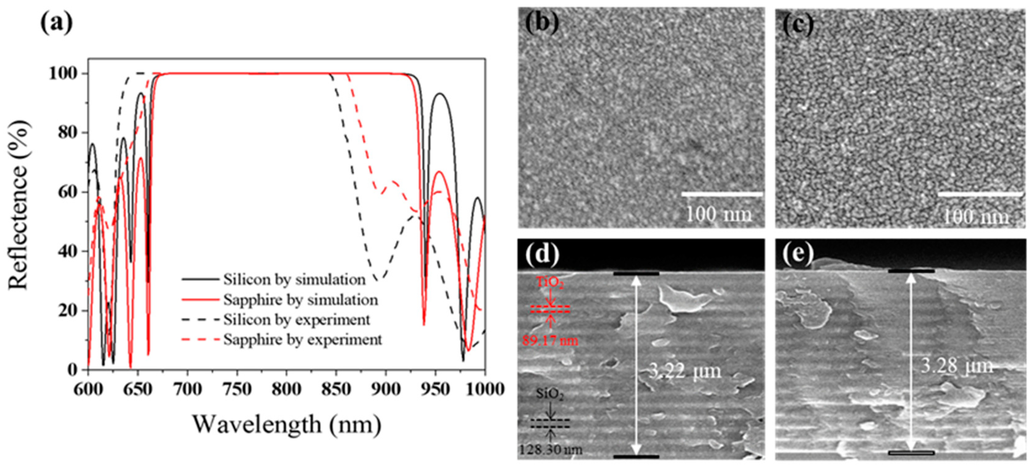
3.1. Characteristics of DBR

The simulation and experiment reflectance results of the top and bottom DBR are shown in Figure 2a. The results have shown that the theoretical reflectance of the top and bottom DBR could achieve 100% at a wide stop-band range from 650 to 850 nm and the center wavelength at 750 nm, which is close to the fluorescence wavelength of FAMACsPb(Br0.1I0.9)3, as shown in Figure 3a. The experiment results still exhibit high reflectance, and the stop band remains the same as in the simulation results. After applying UVO cleaner, SEM was used to assess whether the topography of the DBRs had been altered. The SEM image reveals that the surface (Figure 2b,c) and thickness (Figure 2d,e) of DBRs are identical after using it. The cross-section of the DBR shows that the actual thickness of TiO2 is 89.17 nm, and SiO2 is 128.3 nm, which closely aligns with the simulated conditions. We believe that the slight variation in the thickness of these two dielectric layers compared with the simulation results is the reason for the slight blue shift observed in the actual reflectance compared with the simulated values.

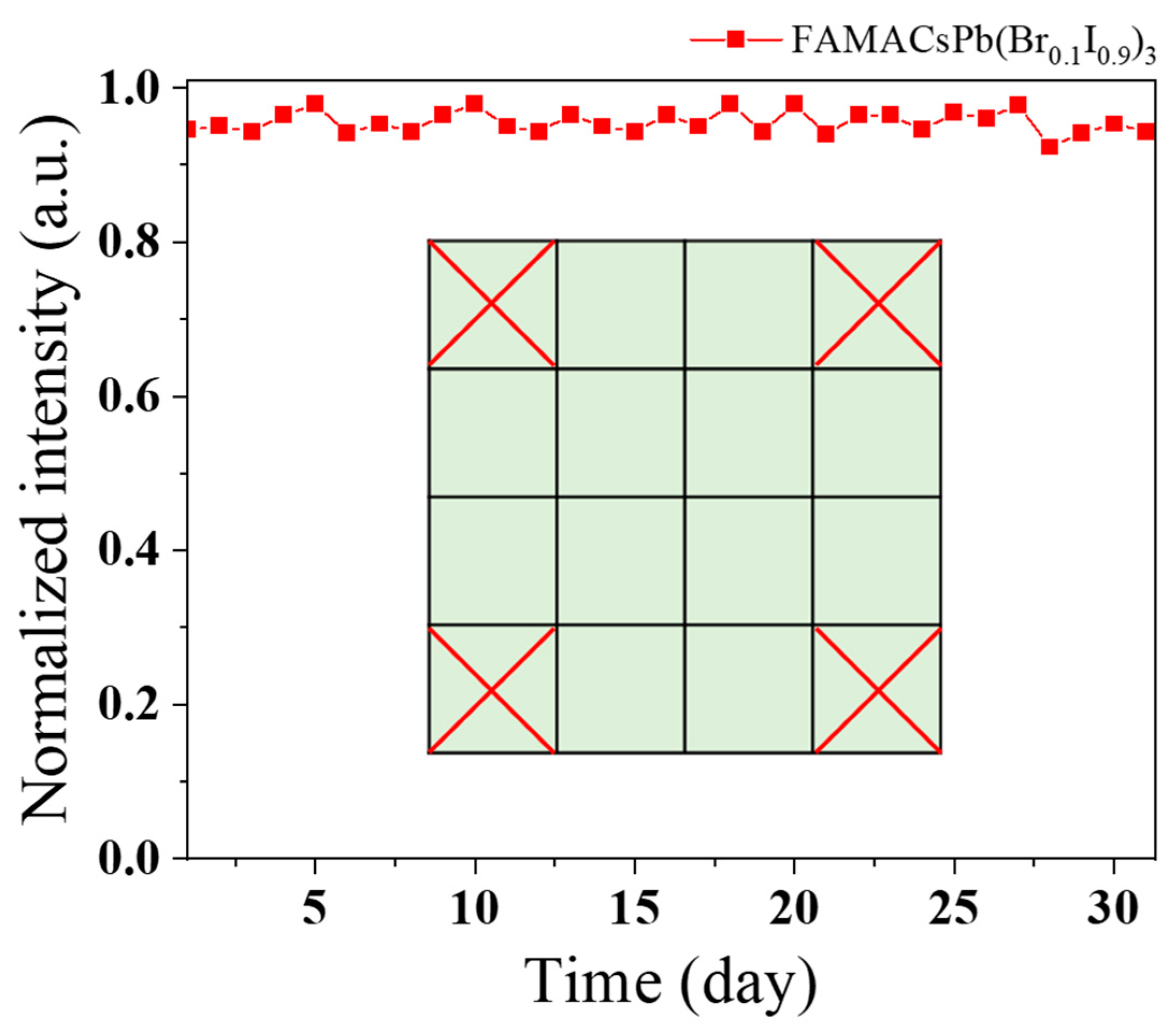
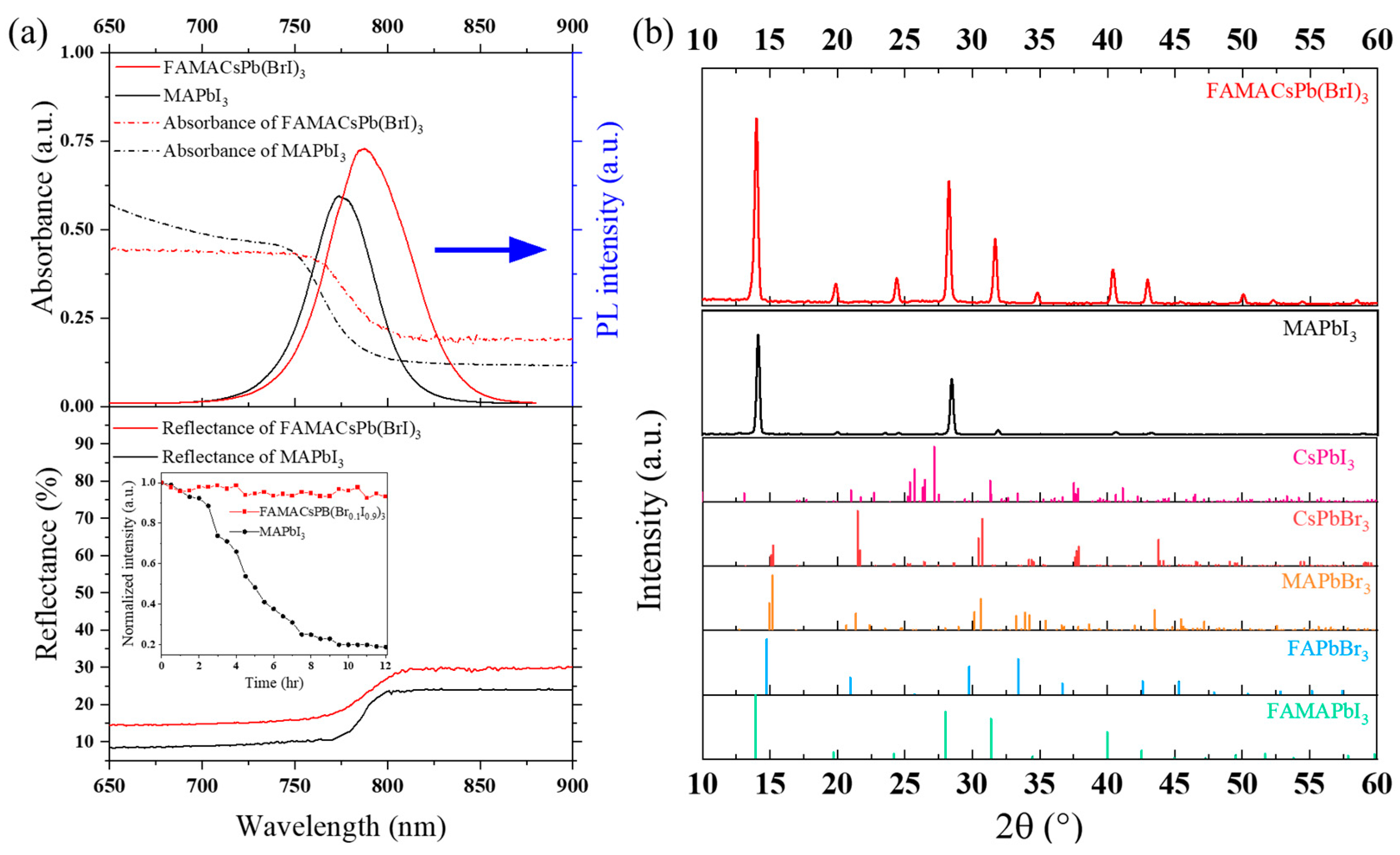
3.2. Properties of FAMACsPb(Br0.1I0.9)3

The FAMACsPb(Br0.1I0.9)3 is spin-coated onto the sapphire substrate, and so is the MAPbI3. To quantify the characteristics of these two materials, we measured their absorption and PL spectra, as shown in Figure 3a. Under the same excitation power, FAMACsPb(Br0.1I0.9)3 possesses a broader gain spectrum and higher emission intensity.
The stability test over several hours for FAMACsPb(Br0.1I0.9)3 and MAPbI3 is depicted in the lower section of Figure 3a. During the stability test, the environmental temperature was at 30 °C, with humidity at approximately 50~60%. After approximately 10 h, the intensity of the MAPbI3 decreased by 20% compared with the original sample, while the intensity of the FAMACsPb(Br0.1I0.9)3 remained consistent and could be sustained for up to one month (see Appendix A).
We also used an X-ray diffractometer (XRD) to confirm the successful synthesis of the triple-cation perovskite and MAPbI3, as shown in Figure 3b. The XRD results are consistent with previous studies [60,61,62,63,64,65,66]. As seen in Figure 3d,f, SEM images of the FAMACsPb(Br0.1I0.9)3 reveal consistent grain sizes, fewer defects, and a greater thickness compared with MAPbI3 (Figure 3c,e). For SEM images and cross-section images with a larger scope and statistical data on grain sizes, refer to Appendix B. A film with these properties can reduce the non-radiative recombination probability [67,68,69,70], thereby increasing the quantum efficiency (QE). Additionally, a thicker gain material can provide a higher optical gain [71,72]. Therefore, we have demonstrated that while the center wavelength of FAMACsPb(Br0.1I0.9)3 is similar to that of MAPbI3, it offers superior film quality and a broader gain spectrum. Leveraging these advantages, FAMACsPb(Br0.1I0.9)3 is a more favorable choice as a gain material when constructing a tunable laser.
As mentioned above, silicon was employed as the substrate for the bottom DBR to prevent light penetration, and the final layer of the bottom DBR is TiO2. We spin-coated the perovskite material onto the last layer of TiO2 on the bottom DBR. This substrate differs from the one used in previous measurements of the material properties of FAMACsPb(Br0.1I0.9)3. To ensure the successful spin-coating of perovskite onto the TiO2 layer, we conducted SEM observations in both top view and cross-section to assess whether there are differences in grain size and thickness compared with when it was spin-coated onto sapphire. The initial surface and thickness of the bottom DBR is shown in Figure 4a,d. FAMACsPb(Br0.1I0.9)3 is spin-coated in the center of the DBR with an area of 1 × 1 cm2, defined by the polyimide tape. The grain size (Figure 4b) and thickness (Figure 4e) are not affected by the tape. A mask is covering it to avoid perovskite destruction. Figure 4c,f illustrate that the grain size and thickness of the perovskite remain similar, suggesting that our mask effectively shields the perovskite from any detrimental effects during the deposition process. For larger-area SEM images and grain size statistics corresponding to the material spin-coated onto the DBR (Figure 4b) and post-E-beam evaporation (Figure 4c), please refer to Appendix C.

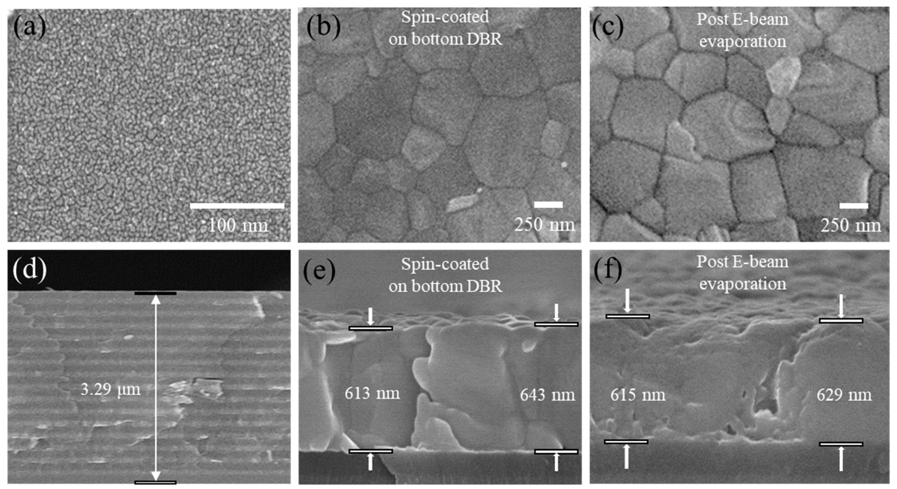
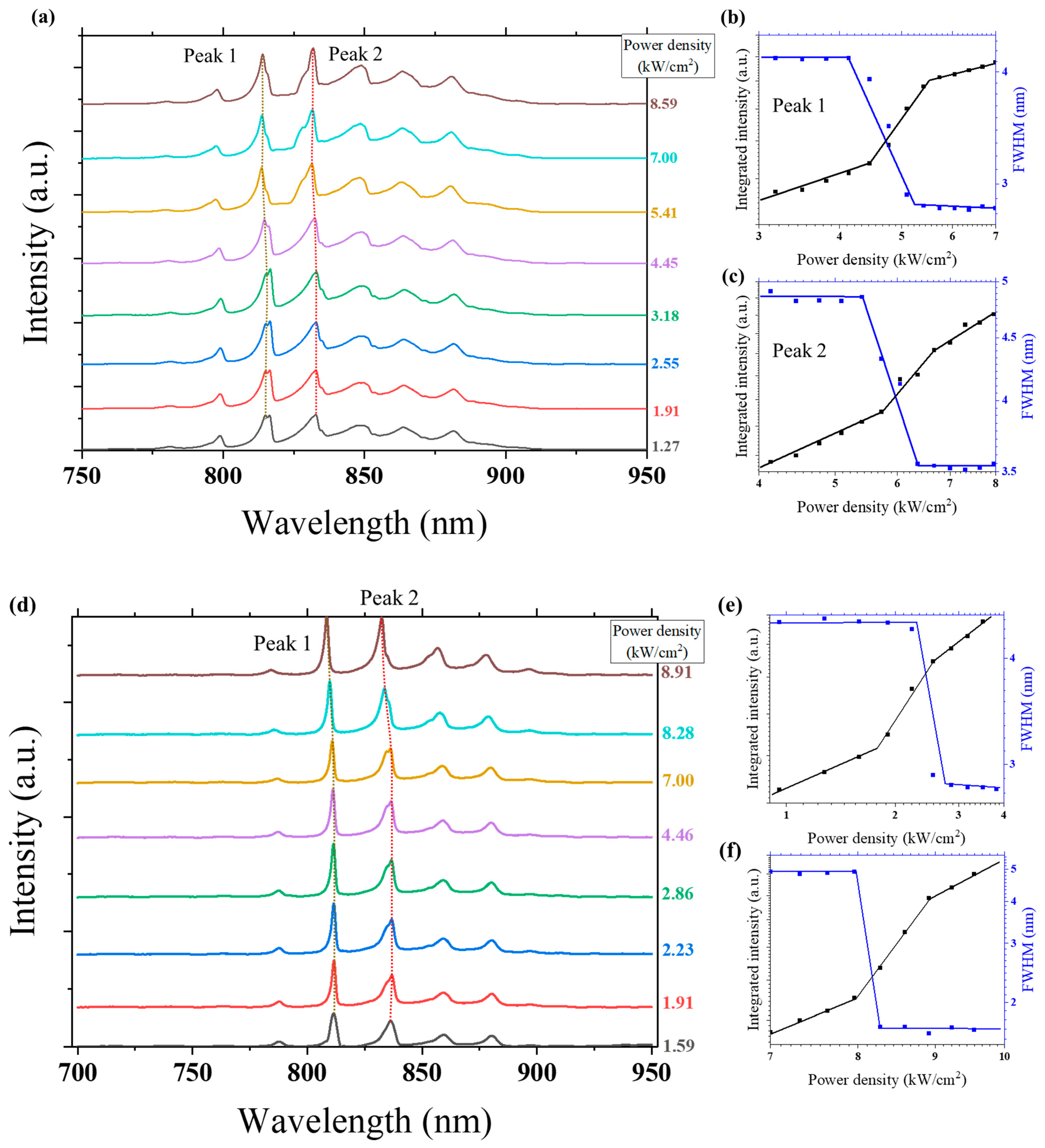
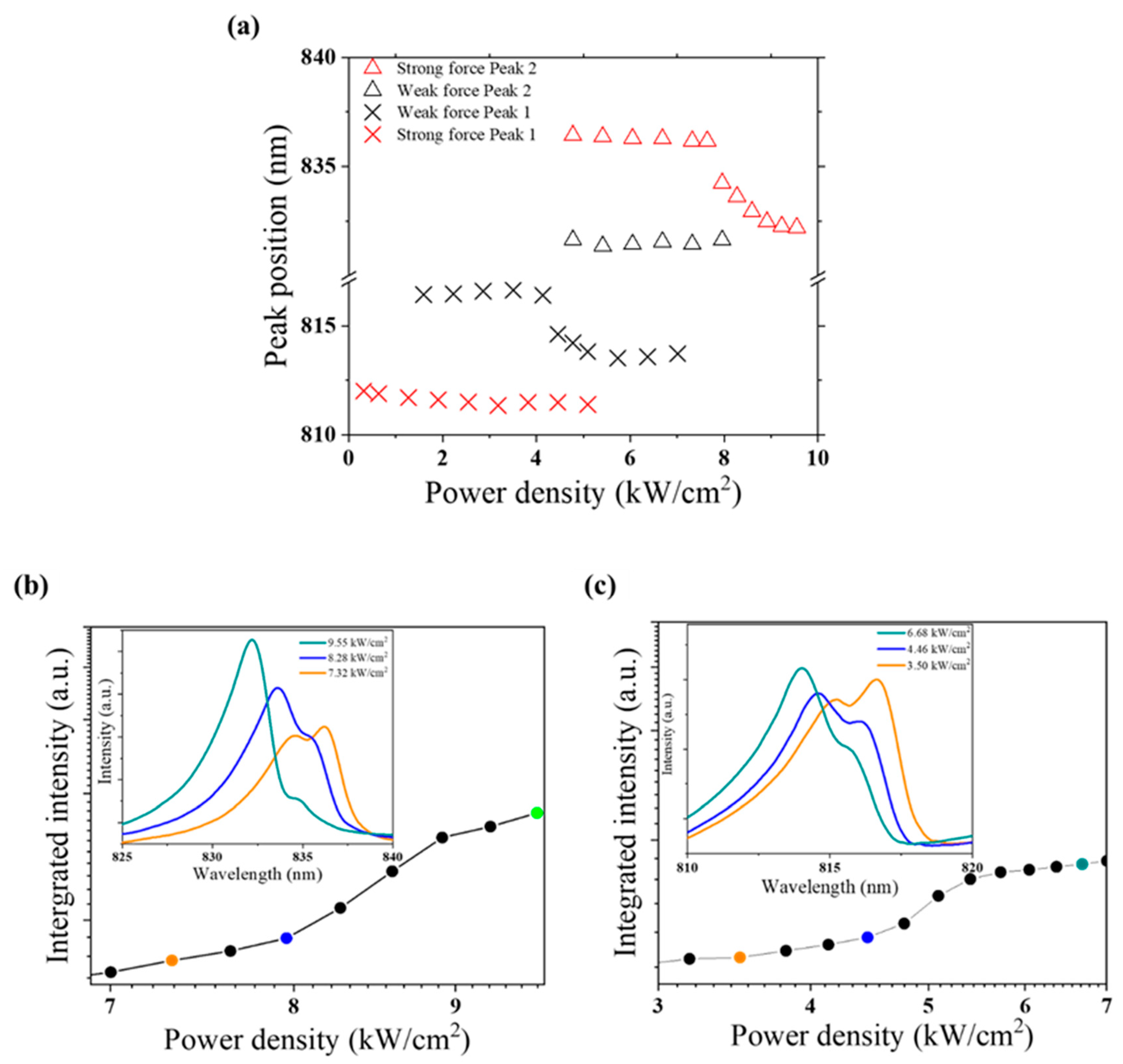
3.3. Properties of Cavity3

The tunable cavity-length VCSEL is fabricated by applying different pressures on the DBR. To better comprehend the performance of the device, PL spectrums excited by 532 nm continuous-wave laser at room temperature in an ambient environment are measured. Figure 5a shows the PL spectra of the device when applying a weak pressure (8.428 N/cm2) on the cavity; the cavity length shrinks to 7.99 μm. As shown in Figure 5b,c, the emission from the laser device exhibits a narrow PL peak 1 located at 813.5 nm (FWHM ≈ 2.82 nm) and peak 2 at 831.3 nm (FWHM ≈ 3.67 nm). The lasing character of the VCSEL is evidenced by the power dependence of the integrated emission intensity (Figure 5e,f). The lasing threshold is estimated to be 4.6 and 6 kW/cm2. The quality factors (Q factor) of the lasing mode are 289.56 and 226.95, respectively.
A stronger pressure (19.698 N/cm2) is further applied on the device, as shown in Figure 5d. The cavity length drops down to 5.79 μm. The emission from the laser device exhibits a narrower PL peak and fewer modes compared with the weak pressure. Peak 1 is located at 811.3 nm (FWHM ≈ 2.83 nm) and peak 2 at 832.2 nm (FWHM ≈ 1.75 nm). The lasing character of the VCSEL is also evidenced by the power dependence of the integrated emission intensity (Figure 5e,f). The lasing threshold is estimated to be 2.9 and 8.2 kW/cm2, while the Q factor of the lasing mode is 286.37 and 476.70, respectively.

4. Discussion

In this study, we compared the optical properties and stability of triple-cation perovskites with the commonly used unary perovskite, MAPbI3. The triple-cation perovskites exhibited superior optical characteristics and stability. In contrast, unary perovskites, such as MAPbX3 (X = Cl, Br, I), tend to rapidly degrade into solid and gaseous byproducts due to thermal fluctuations and humidity exposure [73,74]. Binary perovskites, such as those based on a combination of formamidinium (FA) and methylammonium (MA), such as FAMAPbX3 (X = Br, I), have shown improved thermal stability [37,75,76]. This improvement can be attributed to the larger ionic radius of FA and the presence of dual-ammonium groups, which hinder ion movement within the PbI6 surroundings [77]. However, FA + is susceptible to high hygroscopicity [78], making it prone to degradation in humid environments. Studies have indicated that the addition of cesium ions ( Cs + ) can enhance the overall stability, crystal growth, and morphology [37,39]. The refractive index (n) of the FAMACsPb(Br0.1I0.9)3 can be derived from the absorption and reflectivity spectra (Figure 3a) using the absorption formula [79]
α = 4 π k λ
and reflectivity formula [80]
R = ( n 1 ) 2 + k 2 ( n + 1 ) 2 + k 2
The refractive index (n) is around 2.59 at 800 nm, which is similar to a previous study [81].
The mode characteristics are shown in Table 1. The cavity length is calculated from the formula
L = λ 0 2 2 n Δ λ
where L is the cavity length, λ 0 is the center wavelength, Δ λ is the average mode spacing, and n is the refractive index of the FAMACsPb(Br0.1I0.9)3. Through Table 1, it is observed that the greater the pressure we applied, the shorter the cavity length was, and with appropriate cavity length, we achieve a low threshold, multimode, and high-Q-factor laser.
We observed a slight shift in the peak when increasing the excitation intensity. The peak shifting spectra of the two different forces are plotted in Figure 6a, which shows the peak position for different power densities. Through Figure 6a, two significant gaps appear in the strong force at peak 2 (red triangle) and weak force at peak 1 (black cross). The typical emission spectra of these peaks are depicted in Figure 6b,c. From Figure 6b (weak force peak 2/black cross), we show the emission for three power densities, below (orange) and above (blue) the lasing threshold and saturation (dark cyan). Peaks can be identified at 816 nm, 814 nm, and 813 nm, respectively. The mutual rise and fall of these peaks are due to mode competition. Mode competition occurs when the cavity can allow multiple modes to exist [82]. The modes compete with each other in terms of gain. In the main panel of Figure 6b, the ratio between the two lasing peaks is plotted versus the power density to illustrate mode competition. The orange/blue/dark cyan curve in the inset corresponds to the same experimental points in the main panel. Similarly, through Figure 6c (red triangle), we also we show the emission for three power densities, below (orange) and above (blue) the lasing threshold and saturation (dark cyan). Peaks can also be identified at 836 nm, 833 nm, and 832 nm, respectively.

5. Conclusions

We have demonstrated that FAMACsPb(Br0.1I0.9)3 can serve as a viable gain material in VCSELs, thanks to its exceptional optical properties and thermal stability. This enables it to be excited by continuous-wave (CW) lasers and operate at room temperature under ambient conditions. Notably, FAMACsPb(Br0.1I0.9)3 exhibits superior film quality compared with MAPbI3, allowing for a finer light guidance and reduced excitation energy requirements. Its uniform, and its larger grain size also contributes to lower scattering losses. Furthermore, our material can form thicker films within the same synthesis time, providing an enhanced optical gain. In addition to its stability, FAMACsPb(Br0.1I0.9)3 maintains its illumination capabilities even after a month, highlighting its remarkable durability. Our cavity fabrication approach prevents damage to the gain material during the subsequent DBR deposition. We can also control the optical mode by applying external forces to adjust the cavity length. To expedite cavity length control, we are investigating the incorporation of a piezoelectric stage in our future research. This will allow us to precisely manipulate the cavity length and eliminate mode competition. Our research presents a straightforward and reliable method for fabricating perovskite lasers. The lasing wavelength of our device falls within the infrared region, making it suitable for therapeutic applications in human tissues. By tuning its emission wavelength, it can also be employed in free-space optical communication (FSO) for satellite-based applications [83,84,85,86].

Author Contributions

Writing—original draft preparation, data curation, validation, and formal analysis, C.-C.L.; conceptualization, methodology, investigation, software, and formal analysis, P.-W.C.; resources, funding acquisition, and writing—review and editing, P.C.; investigation and validation, Z.Y.W.; resources, funding acquisition, and writing—review and editing, H.-C.H.; resources and funding acquisition, W.-C.L.; conceptualization, resources, writing—review and editing, supervision, project administration, and funding acquisition, Y.-H.C. All authors have read and agreed to the published version of the manuscript.

Funding

This research was funded by the Young Scholar Fellowship Program by Ministry of Science and Technology (MOST) in Taiwan, under Grant MOST 111-2636-M-006-025. The authors are grateful for the research grant from the MOST (MOST 111-2113-M-006-009, MOST 111-2221-E-006-061-MY2, MOST 111-2112-M-006-023-MY3). This work was also financially supported by the Hierarchical Green-Energy Materials (Hi-GEM) Research Center, from The Featured Areas Research Center Program within the framework of the Higher Education Sprout Project by the Ministry of Education (MOE) in Taiwan. This research was supported in part by the Higher Education Sprout Project, Ministry of Education to the Headquarter of University Advancement at National Cheng Kung University (NCKU).

Data Availability Statement

The data that support the findings of this study are available from the corresponding authors upon reasonable request.

Acknowledgments

The authors gratefully acknowledge the use of E-beam and UV-Vis-NIR from Jinn-Kong Sheu and Tzung-Fang Guo and XRD005102 and EM003600 of the equipment belonging to the Core Facility Center of National Cheng Kung University.

Conflicts of Interest

The authors declare no conflict of interest.

Appendix A

To ensure the precision of our experiments, we maintained a fixed laser power intensity of 0.32 kW/cm2 and a sensor integration time of 0.3 s within our PL measurement system. Simultaneously, we standardized all the parameters of the spectrometer. To correct for potential errors induced by external environmental factors, we employed gallium arsenide (GaAs) wafers as reference samples and performed weekly corrections to our recorded light intensities. Throughout the extended stability testing of FAMACsPb(Br0.1I0.9)3, the material was exposed to an environmental temperature at 30 °C, with humidity at approximately 50~60%. The substrate was divided into 16 distinct regions, as depicted in Figure A1. After excluding the four corner regions, we conducted daily scans and recorded the strongest signal for light intensity in each region. From the resulting dataset of 12 values, we excluded the maximum and minimum values, then calculated the average of the remaining 10 data points as the recorded light intensity for that day. Finally, the average daily light intensity measurements were plotted against time, as illustrated in Figure A1.
Figure A1. Stability test of FAMACsPb(Br0.1I0.9)3 for a month. Inside A1 is the diagram of how we measured the average PL intensity.
Crystals 13 01517 g0a1

Appendix B

The comparison of the large-area SEM images and cross-sectional images of MAPbI3 and FAMACsPb(Br0.1I0.9)3 spin-coated onto sapphire is shown in Figure A2a,b. From the figures, we can observe that MAPbI3 exhibits noticeable defects when observed at a lower magnification. It can be reasonably inferred that when we magnify the images, MAPbI3 will reveal even more defects. Although FAMACsPb(BrI0.9)3 also has defects, we believe that its film quality is significantly better than that of MAPbI3. Figure A2c,d represent the statistical histograms of grain sizes based on Figure A2a,b. From Figure A2c, it can be observed that the grain sizes of MAPbI3 range from tens of nanometers to nearly 1 μm, indicating an uneven grain distribution. This may lead to reduced gain and light scattering during PL measurements, resulting in a reduced light intensity. This observation is further confirmed by the lower PL intensity compared with FAMACsPb(BrI0.9)3 (see Figure 3a). In contrast, FAMACsPb(Br0.1I0.9)3 exhibits relatively consistent grain sizes, ranging from approximately 200 nm to 300 nm. Based on these statistical findings, we selected FAMACsPb(Br0.1I0.9)3 for its uniform film quality and relatively consistent grain size as the gain medium in our resonant cavity.
Figure A2. Large-area SEM and cross-section of (a) MAPbI3 and (b) FAMACsPb(Br0.1I0.9)3. (c,d) Grain size distribution derived from (a,b).
Crystals 13 01517 g0a2

Appendix C

To verify whether the grain size of our FAMACsPb(Br0.1I0.9)3 film spun onto TiO2 is similar to that spun onto sapphire, we conducted SEM imaging and grain size measurements on the TiO2 substrate sample. According to the statistical results shown in Figure A3c, we found that the grain sizes on TiO2 are similar to those on sapphire, with sizes concentrated between 200 and 300 nm. Additionally, after applying a custom-made mask and undergoing the E-beam evaporation process, we also performed grain size measurements to confirm if this process affected the grain size. As depicted in Figure A3d, the distribution of grain sizes remained consistent with the pre-evaporation measurements. The icon in the upper right corner of Figure A3a,b represents the current process, and the whole process flow refers to Figure 1a.
Figure A3. Large-area SEM of (a) FAMACsPb(Br0.1I0.9)3 spin-coated onto the TiO2. (b) FAMACsPb(Br0.1I0.9)3 after E-beam evaporation. (c,d) Grain size distribution derived from (a,b).
Crystals 13 01517 g0a3

References

  1. Alhilal, A.; Finley, B.; Braud, T.; Su, D.; Hui, P. Distributed vehicular computing at the dawn of 5G: A survey. arXiv 2020, arXiv:2001.07077. [Google Scholar]
  2. Alimi, I.A.; Teixeira, A.L.; Monteiro, P.P. Toward an efficient C-RAN optical fronthaul for the future networks: A tutorial on technologies, requirements, challenges, and solutions. IEEE Commun. Surv. Tutor. 2017, 20, 708–769. [Google Scholar] [CrossRef]
  3. Jung, P.; Baier, P.W.; Steil, A. Advantages of CDMA and spread spectrum techniques over FDMA and TDMA in cellular mobile radio applications. IEEE Trans. Veh. Technol. 1993, 42, 357–364. [Google Scholar] [CrossRef]
  4. Turin, G.L. Introduction to spread-spectrum antimultipath techniques and their application to urban digital radio. Proc. IEEE 1980, 68, 328–353. [Google Scholar] [CrossRef]
  5. Pickholtz, R.; Schilling, D.; Milstein, L. Theory of spread-spectrum communications-a tutorial. IEEE Trans. Commun. 1982, 30, 855–884. [Google Scholar] [CrossRef]
  6. Sacher, W.; Green, W.; Assefa, S.; Barwicz, T.; Pan, H.; Shank, S.; Vlasov, Y.; Poon, J. Coupling modulation of microrings at rates beyond the linewidth limit. Opt. Express 2013, 21, 9722–9733. [Google Scholar] [CrossRef]
  7. Dedieu, H.; Kennedy, M.P.; Hasler, M. Chaos shift keying: Modulation and demodulation of a chaotic carrier using self-synchronizing Chua's circuits. IEEE Trans. Circuits Syst. II Analog Digit. Signal Process. 1993, 40, 634–642. [Google Scholar] [CrossRef]
  8. Cuomo, K.M.; Oppenheim, A.V.; Strogatz, S.H. Synchronization of Lorenz-based chaotic circuits with applications to communications. IEEE Trans. Circuits Syst. II Analog Digit. Signal Process. 1993, 40, 626–633. [Google Scholar] [CrossRef]
  9. Wang, W.-Q.; So, H.C.; Farina, A. An overview on time/frequency modulated array processing. IEEE J. Sel. Top. Signal Process. 2016, 11, 228–246. [Google Scholar] [CrossRef]
  10. Wan, Y.; Zhang, S.; Norman, J.C.; Kennedy, M.; He, W.; Tong, Y.; Shang, C.; He, J.J.; Tsang, H.K.; Gossard, A.C. Directly modulated single-mode tunable quantum dot lasers at 1.3 µm. Laser Photonics Rev. 2020, 14, 1900348. [Google Scholar] [CrossRef]
  11. Dagli, N. Wide-bandwidth lasers and modulators for RF photonics. IEEE Trans. Microw. Theory Tech. 1999, 47, 1151–1171. [Google Scholar] [CrossRef]
  12. Tang, J.; Lane, P.; Shore, K.A. High-speed transmission of adaptively modulated optical OFDM signals over multimode fibers using directly modulated DFBs. J. Light. Technol. 2006, 24, 429. [Google Scholar] [CrossRef]
  13. Bjork, G.; Yamamoto, Y. Analysis of semiconductor microcavity lasers using rate equations. IEEE J. Quantum Electron. 1991, 27, 2386–2396. [Google Scholar] [CrossRef]
  14. Duarte, F.J. Tunable Laser Optics; CRC Press: Boca Raton, FL, USA, 2017. [Google Scholar]
  15. Jiang, X.F.; Zou, C.L.; Wang, L.; Gong, Q.; Xiao, Y.F. Whispering-gallery microcavities with unidirectional laser emission. Laser Photonics Rev. 2016, 10, 40–61. [Google Scholar] [CrossRef]
  16. He, L.; Özdemir, Ş.K.; Yang, L. Whispering gallery microcavity lasers. Laser Photonics Rev. 2013, 7, 60–82. [Google Scholar] [CrossRef]
  17. Mi, Y.; Liu, Z.; Shang, Q.; Niu, X.; Shi, J.; Zhang, S.; Chen, J.; Du, W.; Wu, Z.; Wang, R. Fabry–Pérot Oscillation and Room Temperature Lasing in Perovskite Cube-Corner Pyramid Cavities. Small 2018, 14, 1703136. [Google Scholar] [CrossRef] [PubMed]
  18. Ma, R.M.; Oulton, R.F.; Sorger, V.J.; Zhang, X. Plasmon lasers: Coherent light source at molecular scales. Laser Photonics Rev. 2013, 7, 1–21. [Google Scholar] [CrossRef]
  19. Pauzauskie, P.J.; Sirbuly, D.J.; Yang, P. Semiconductor nanowire ring resonator laser. Phys. Rev. Lett. 2006, 96, 143903. [Google Scholar] [CrossRef]
  20. Lee, M.M.; Teuscher, J.; Miyasaka, T.; Murakami, T.N.; Snaith, H.J. Efficient hybrid solar cells based on meso-superstructured organometal halide perovskites. Science 2012, 338, 643–647. [Google Scholar] [CrossRef]
  21. Leijtens, T.; Eperon, G.E.; Pathak, S.; Abate, A.; Lee, M.M.; Snaith, H.J. Overcoming ultraviolet light instability of sensitized TiO2 with meso-superstructured organometal tri-halide perovskite solar cells. Nat. Commun. 2013, 4, 2885. [Google Scholar] [CrossRef]
  22. Tan, Z.-K.; Moghaddam, R.S.; Lai, M.L.; Docampo, P.; Higler, R.; Deschler, F.; Price, M.; Sadhanala, A.; Pazos, L.M.; Credgington, D. Bright light-emitting diodes based on organometal halide perovskite. Nat. Nanotechnol. 2014, 9, 687–692. [Google Scholar] [CrossRef]
  23. Manser, J.S.; Kamat, P.V. Band filling with free charge carriers in organometal halide perovskites. Nat. Photonics 2014, 8, 737–743. [Google Scholar] [CrossRef]
  24. Yu, Z.; Sun, L. Recent progress on hole-transporting materials for emerging organometal halide perovskite solar cells. Adv. Energy Mater. 2015, 5, 1500213. [Google Scholar] [CrossRef]
  25. Dong, C.; Wang, Z.-K.; Liao, L.-S. Progress of triple cation organometal halide perovskite solar cells. Energy Technol. 2020, 8, 1900804. [Google Scholar] [CrossRef]
  26. Zhu, H.; Fu, Y.; Meng, F.; Wu, X.; Gong, Z.; Ding, Q.; Gustafsson, M.V.; Trinh, M.T.; Jin, S.; Zhu, X. Lead halide perovskite nanowire lasers with low lasing thresholds and high quality factors. Nat. Mater. 2015, 14, 636–642. [Google Scholar] [CrossRef]
  27. Frost, J.M.; Butler, K.T.; Brivio, F.; Hendon, C.H.; Van Schilfgaarde, M.; Walsh, A. Atomistic origins of high-performance in hybrid halide perovskite solar cells. Nano Lett. 2014, 14, 2584–2590. [Google Scholar] [CrossRef]
  28. De Wolf, S.; Holovsky, J.; Moon, S.-J.; Loper, P.; Niesen, B.; Ledinsky, M.; Haug, F.-J.; Yum, J.-H.; Ballif, C. Organometallic halide perovskites: Sharp optical absorption edge and its relation to photovoltaic performance. J. Phys. Chem. Lett. 2014, 5, 1035–1039. [Google Scholar] [CrossRef]
  29. Zhang, W.; Wang, Y.C.; Li, X.; Song, C.; Wan, L.; Usman, K.; Fang, J. Recent advance in solution-processed organic interlayers for high-performance planar perovskite solar cells. Adv. Sci. 2018, 5, 1800159. [Google Scholar] [CrossRef]
  30. Deng, Y.; Peng, E.; Shao, Y.; Xiao, Z.; Dong, Q.; Huang, J. Scalable fabrication of efficient organolead trihalide perovskite solar cells with doctor-bladed active layers. Energy Environ. Sci. 2015, 8, 1544–1550. [Google Scholar] [CrossRef]
  31. Kim, J.; Lee, S.-H.; Lee, J.H.; Hong, K.-H. The role of intrinsic defects in methylammonium lead iodide perovskite. J. Phys. Chem. Lett. 2014, 5, 1312–1317. [Google Scholar] [CrossRef]
  32. Becker, M.; Wark, M. Controlling the crystallization and grain size of sequentially deposited planar perovskite films via the permittivity of the conversion solution. Org. Electron. 2017, 50, 87–93. [Google Scholar] [CrossRef]
  33. Gratzel, M. The rise of highly efficient and stable perovskite solar cells. Acc. Chem. Res. 2017, 50, 487–491. [Google Scholar] [CrossRef] [PubMed]
  34. Jang, D.M.; Park, K.; Kim, D.H.; Park, J.; Shojaei, F.; Kang, H.S.; Ahn, J.-P.; Lee, J.W.; Song, J.K. Reversible halide exchange reaction of organometal trihalide perovskite colloidal nanocrystals for full-range band gap tuning. Nano Lett. 2015, 15, 5191–5199. [Google Scholar] [CrossRef] [PubMed]
  35. Xing, G.; Mathews, N.; Lim, S.S.; Yantara, N.; Liu, X.; Sabba, D.; Grätzel, M.; Mhaisalkar, S.; Sum, T.C. Low-temperature solution-processed wavelength-tunable perovskites for lasing. Nat. Mater. 2014, 13, 476–480. [Google Scholar] [CrossRef]
  36. Ava, T.T.; Al Mamun, A.; Marsillac, S.; Namkoong, G. A review: Thermal stability of methylammonium lead halide based perovskite solar cells. Appl. Sci. 2019, 9, 188. [Google Scholar] [CrossRef]
  37. Saliba, M.; Matsui, T.; Seo, J.-Y.; Domanski, K.; Correa-Baena, J.-P.; Nazeeruddin, M.K.; Zakeeruddin, S.M.; Tress, W.; Abate, A.; Hagfeldt, A. Cesium-containing triple cation perovskite solar cells: Improved stability, reproducibility and high efficiency. Energy Environ. Sci. 2016, 9, 1989–1997. [Google Scholar] [CrossRef]
  38. Smecca, E.; Numata, Y.; Deretzis, I.; Pellegrino, G.; Boninelli, S.; Miyasaka, T.; La Magna, A.; Alberti, A. Stability of solution-processed MAPbI 3 and FAPbI 3 layers. Phys. Chem. Chem. Phys. 2016, 18, 13413–13422. [Google Scholar] [CrossRef]
  39. Niu, G.; Li, W.; Li, J.; Liang, X.; Wang, L. Enhancement of thermal stability for perovskite solar cells through cesium doping. RSC Adv. 2017, 7, 17473–17479. [Google Scholar] [CrossRef]
  40. Singh, T.; Miyasaka, T. Stabilizing the efficiency beyond 20% with a mixed cation perovskite solar cell fabricated in ambient air under controlled humidity. Adv. Energy Mater. 2018, 8, 1700677. [Google Scholar] [CrossRef]
  41. Yang, W.; Su, R.; Luo, D.; Hu, Q.; Zhang, F.; Xu, Z.; Wang, Z.; Tang, J.; Lv, Z.; Yang, X. Surface modification induced by perovskite quantum dots for triple-cation perovskite solar cells. Nano Energy 2020, 67, 104189. [Google Scholar] [CrossRef]
  42. Available online: https://www.nrel.gov/index.html (accessed on 21 March 2023).
  43. Zhang, Q.; Shang, Q.; Su, R.; Do, T.T.H.; Xiong, Q. Halide perovskite semiconductor lasers: Materials, cavity design, and low threshold. Nano Lett. 2021, 21, 1903–1914. [Google Scholar] [CrossRef] [PubMed]
  44. Dong, H.; Zhang, C.; Liu, X.; Yao, J.; Zhao, Y.S. Materials chemistry and engineering in metal halide perovskite lasers. Chem. Soc. Rev. 2020, 49, 951–982. [Google Scholar] [CrossRef] [PubMed]
  45. Chen, S.; Zhang, C.; Lee, J.; Han, J.; Nurmikko, A. High-Q, low-threshold monolithic perovskite thin-film vertical-cavity lasers. Adv. Mater. 2017, 29, 1604781. [Google Scholar] [CrossRef]
  46. Wang, J.; Su, R.; Xing, J.; Bao, D.; Diederichs, C.; Liu, S.; Liew, T.C.; Chen, Z.; Xiong, Q. Room temperature coherently coupled exciton–polaritons in two-dimensional organic–inorganic perovskite. ACS Nano 2018, 12, 8382–8389. [Google Scholar] [CrossRef]
  47. Huang, C.-Y.; Zou, C.; Mao, C.; Corp, K.L.; Yao, Y.-C.; Lee, Y.-J.; Schlenker, C.W.; Jen, A.K.; Lin, L.Y. CsPbBr3 perovskite quantum dot vertical cavity lasers with low threshold and high stability. Acs Photonics 2017, 4, 2281–2289. [Google Scholar] [CrossRef]
  48. Liu, Y.; Yang, W.; Xiao, S.; Zhang, N.; Fan, Y.; Qu, G.; Song, Q. Surface-emitting perovskite random lasers for speckle-free imaging. ACS Nano 2019, 13, 10653–10661. [Google Scholar] [CrossRef] [PubMed]
  49. Chen, S.; Nurmikko, A. Stable green perovskite vertical-cavity surface-emitting lasers on rigid and flexible substrates. ACS Photonics 2017, 4, 2486–2494. [Google Scholar] [CrossRef]
  50. Alias, M.S.; Liu, Z.; Al-Atawi, A.; Ng, T.K.; Wu, T.; Ooi, B.S. Continuous-wave optically pumped green perovskite vertical-cavity surface-emitter. Opt. Lett. 2017, 42, 3618–3621. [Google Scholar] [CrossRef]
  51. Zhang, Q.; Ha, S.T.; Liu, X.; Sum, T.C.; Xiong, Q. Room-temperature near-infrared high-Q perovskite whispering-gallery planar nanolasers. Nano Lett. 2014, 14, 5995–6001. [Google Scholar] [CrossRef]
  52. Mi, Y.; Zhong, Y.; Zhang, Q.; Liu, X. Continuous-wave pumped perovskite lasers. Adv. Opt. Mater. 2019, 7, 1900544. [Google Scholar] [CrossRef]
  53. Zhu, Y.; Qin, Q.; Xu, F.; Fan, F.; Ding, Y.; Zhang, T.; Wiley, B.J.; Wang, Z.L. Size effects on elasticity, yielding, and fracture of silver nanowires: In situ experiments. Phys. Rev. B 2012, 85, 045443. [Google Scholar] [CrossRef]
  54. Chueh, C.-C.; Li, C.-Z.; Jen, A.K.-Y. Recent progress and perspective in solution-processed Interfacial materials for efficient and stable polymer and organometal perovskite solar cells. Energy Environ. Sci. 2015, 8, 1160–1189. [Google Scholar] [CrossRef]
  55. Wang, Z.; Fang, J.; Mi, Y.; Zhu, X.; Ren, H.; Liu, X.; Yan, Y. Enhanced performance of perovskite solar cells by ultraviolet-ozone treatment of mesoporous TiO2. Appl. Surf. Sci. 2018, 436, 596–602. [Google Scholar] [CrossRef]
  56. Park, J.H.; Seo, J.; Park, S.; Shin, S.S.; Kim, Y.C.; Jeon, N.J.; Shin, H.W.; Ahn, T.K.; Noh, J.H.; Yoon, S.C. Efficient CH3NH3PbI3 perovskite solar cells employing nanostructured p-type NiO electrode formed by a pulsed laser deposition. Adv. Mater. 2015, 27, 4013–4019. [Google Scholar] [CrossRef]
  57. Xia, R.; Gao, X.X.; Zhang, Y.; Drigo, N.; Queloz, V.I.; Tirani, F.F.; Scopelliti, R.; Huang, Z.; Fang, X.; Kinge, S. An efficient approach to fabricate air-stable perovskite solar cells via addition of a self-polymerizing ionic liquid. Adv. Mater. 2020, 32, 2003801. [Google Scholar] [CrossRef]
  58. Kim, H.; Lee, J.; Kim, B.; Byun, H.R.; Kim, S.H.; Oh, H.M.; Baik, S.; Jeong, M.S. Enhanced stability of MAPbI3 perovskite solar cells using poly (p-chloro-xylylene) encapsulation. Sci. Rep. 2019, 9, 15461. [Google Scholar] [CrossRef]
  59. Kakekhani, A.; Katti, R.N.; Rappe, A.M. Water in hybrid perovskites: Bulk MAPbI3 degradation via super-hydrous state. APL Mater. 2019, 7, 041112. [Google Scholar] [CrossRef]
  60. Wiedemann, D.; Breternitz, J.; Paley, D.W.; Schorr, S. Hybrid perovskite at full tilt: Structure and symmetry relations of the incommensurately modulated phase of methylammonium lead bromide, MAPbBr3. J. Phys. Chem. Lett. 2021, 12, 2358–2362. [Google Scholar] [CrossRef]
  61. Swainson, I.; Hammond, R.; Soullière, C.; Knop, O.; Massa, W. Phase transitions in the perovskite methylammonium lead bromide, CH3ND3PbBr3. J. Solid State Chem. 2003, 176, 97–104. [Google Scholar] [CrossRef]
  62. Li, C.; Juarez-Perez, E.J.; Mayoral, A. Atomic-level understanding of a formamidinium hybrid halide perovskite, FAPbBr 3. Chem. Commun. 2022, 58, 12164–12167. [Google Scholar] [CrossRef]
  63. Huang, Y.; Li, L.; Liu, Z.; Jiao, H.; He, Y.; Wang, X.; Zhu, R.; Wang, D.; Sun, J.; Chen, Q. The intrinsic properties of FA (1− x) MA x PbI 3 perovskite single crystals. J. Mater. Chem. A 2017, 5, 8537–8544. [Google Scholar] [CrossRef]
  64. Stoumpos, C.C.; Malliakas, C.D.; Kanatzidis, M.G. Semiconducting tin and lead iodide perovskites with organic cations: Phase transitions, high mobilities, and near-infrared photoluminescent properties. Inorg. Chem. 2013, 52, 9019–9038. [Google Scholar] [CrossRef]
  65. Stoumpos, C.C.; Malliakas, C.D.; Peters, J.A.; Liu, Z.; Sebastian, M.; Im, J.; Chasapis, T.C.; Wibowo, A.C.; Chung, D.Y.; Freeman, A.J. Crystal growth of the perovskite semiconductor CsPbBr3: A new material for high-energy radiation detection. Cryst. Growth Des. 2013, 13, 2722–2727. [Google Scholar] [CrossRef]
  66. Wang, L.; Wang, X.; Deng, L.-L.; Leng, S.; Guo, X.; Tan, C.-H.; Choy, W.C.; Chen, C.-C. The mechanism of universal green antisolvents for intermediate phase controlled high-efficiency formamidinium-based perovskite solar cells. Mater. Horiz. 2020, 7, 934–942. [Google Scholar] [CrossRef]
  67. Luo, D.; Su, R.; Zhang, W.; Gong, Q.; Zhu, R. Minimizing non-radiative recombination losses in perovskite solar cells. Nat. Rev. Mater. 2020, 5, 44–60. [Google Scholar] [CrossRef]
  68. Azzouzi, M.; Yan, J.; Kirchartz, T.; Liu, K.; Wang, J.; Wu, H.; Nelson, J. Nonradiative energy losses in bulk-heterojunction organic photovoltaics. Phys. Rev. X 2018, 8, 031055. [Google Scholar] [CrossRef]
  69. Bi, P.; Zhang, S.; Chen, Z.; Xu, Y.; Cui, Y.; Zhang, T.; Ren, J.; Qin, J.; Hong, L.; Hao, X. Reduced non-radiative charge recombination enables organic photovoltaic cell approaching 19% efficiency. Joule 2021, 5, 2408–2419. [Google Scholar] [CrossRef]
  70. Long, R.; Fang, W.; Akimov, A.V. Nonradiative electron–hole recombination rate is greatly reduced by defects in monolayer black phosphorus: Ab initio time domain study. J. Phys. Chem. Lett. 2016, 7, 653–659. [Google Scholar] [CrossRef]
  71. Erdem, O.; Foroutan, S.; Gheshlaghi, N.; Guzelturk, B.; Altintas, Y.; Demir, H.V. Thickness-tunable self-assembled colloidal nanoplatelet films enable ultrathin optical gain media. Nano Lett. 2020, 20, 6459–6465. [Google Scholar] [CrossRef]
  72. Pavesi, L.; Dal Negro, L.; Mazzoleni, C.; Franzo, G.; Priolo, d.F. Optical gain in silicon nanocrystals. Nature 2000, 408, 440–444. [Google Scholar] [CrossRef]
  73. Kundu, S.; Kelly, T.L. In situ studies of the degradation mechanisms of perovskite solar cells. EcoMat 2020, 2, e12025. [Google Scholar] [CrossRef]
  74. Yang, J.; Siempelkamp, B.D.; Liu, D.; Kelly, T.L. Investigation of CH3NH3PbI3 degradation rates and mechanisms in controlled humidity environments using in situ techniques. ACS Nano 2015, 9, 1955–1963. [Google Scholar] [CrossRef]
  75. Luo, D.; Yang, W.; Wang, Z.; Sadhanala, A.; Hu, Q.; Su, R.; Shivanna, R.; Trindade, G.F.; Watts, J.F.; Xu, Z. Enhanced photovoltage for inverted planar heterojunction perovskite solar cells. Science 2018, 360, 1442–1446. [Google Scholar] [CrossRef]
  76. Zheng, X.; Chen, B.; Dai, J.; Fang, Y.; Bai, Y.; Lin, Y.; Wei, H.; Zeng, X.C.; Huang, J. Defect passivation in hybrid perovskite solar cells using quaternary ammonium halide anions and cations. Nat. Energy 2017, 2, 17102. [Google Scholar] [CrossRef]
  77. Eperon, G.E.; Stranks, S.D.; Menelaou, C.; Johnston, M.B.; Herz, L.M.; Snaith, H.J. Formamidinium lead trihalide: A broadly tunable perovskite for efficient planar heterojunction solar cells. Energy Environ. Sci. 2014, 7, 982–988. [Google Scholar] [CrossRef]
  78. Li, M.; Li, H.; Fu, J.; Liang, T.; Ma, W. Recent progress on the stability of perovskite solar cells in a humid environment. J. Phys. Chem. C 2020, 124, 27251–27266. [Google Scholar] [CrossRef]
  79. Kavokin, A.V.; Baumberg, J.J.; Malpuech, G.; Laussy, F.P. Microcavities; Oxford University Press: Oxford, UK, 2017. [Google Scholar]
  80. Fox, A.M.; Fox, D.P.A.M. Optical Properties of Solids; Oxford University Press: Oxford, UK, 2001. [Google Scholar]
  81. Tejada, A.; Peters, S.; Al-Ashouri, A.; Turren-Cruz, S.H.; Abate, A.; Albrecht, S.; Ruske, F.; Rech, B.; Guerra, J.A.; Korte, L. Hybrid Perovskite Degradation from an Optical Perspective: A Spectroscopic Ellipsometry Study from the Deep Ultraviolet to the Middle Infrared. Adv. Opt. Mater. 2022, 10, 2101553. [Google Scholar] [CrossRef]
  82. Türeci, H.E.; Stone, A.D.; Collier, B. Self-consistent multimode lasing theory for complex or random lasing media. Phys. Rev. A 2006, 74, 043822. [Google Scholar] [CrossRef]
  83. Beland, R.R. Propagation through atmospheric optical turbulence. Atmos. Propag. Radiat. 1993, 2, 157–232. [Google Scholar]
  84. Kaushal, H.; Kaddoum, G. Free space optical communication: Challenges and mitigation techniques. arXiv 2015, arXiv:1506.04836. [Google Scholar]
  85. Cazaubiel, V.; Planche, G.; Chorvalli, V.; Le Hors, L.; Roy, B.; Giraud, E.; Vaillon, L.; Carré, F.; Decourbey, E. LOLA: A 40,000 km optical link between an aircraft and a geostationary satellite. In Proceedings of the ESA/CNES ICSO 2006, Noordwijk, The Netherlands, 27–30 June 2006. [Google Scholar]
  86. Perlot, N.; Knapek, M.; Giggenbach, D.; Horwath, J.; Brechtelsbauer, M.; Takayama, Y.; Jono, T. Results of the optical downlink experiment KIODO from OICETS satellite to optical ground station Oberpfaffenhofen (OGS-OP). In Proceedings of the Free-Space Laser Communication Technologies XIX and Atmospheric Propagation of Electromagnetic Waves, San Jose, CA, USA, 12 February 2007; Volume 6457, pp. 28–35. [Google Scholar]
Figure 1. (a) Schematics of the procedure for thin film and metal pillars. (b) DBR alignment platform. (c) Schematics of the device. (d) The setup of the PL measurement.
Crystals 13 01517 g001
Figure 2. Characteristics of DBR. (a) Simulated and experimental results of DBR. (b) Surface of DBR before using UVO cleaner. (c) Surface of DBR after using UVO cleaner; the surface topography remains the same compare with (d). (d) Cross-section of DBR before using UVO cleaner. (e) Cross-section of DBR after using UVO cleaner (the slightly different thickness in (d,e) is due to the measurement deviation); the thickness is similar to (d).
Crystals 13 01517 g002
Figure 3. Comparison between MAPbI3 and FAMACsPb(Br0.1I0.9)3. (a) Absorption, PL, and reflectivity spectrum of FAMACsPb(Br0.1I0.9)3 (red curve) and MAPbI3 (black curve). The lower part of (a) is the stability test: the material is placed in ambient conditions with a humidity level of approximately 50–60% for a month. (b) XRD result for FAMACsPb(Br0.1I0.9)3 compared with previous study and MAPbI3. (c,d) SEM of MAPbI3 and FAMACsPb(Br0.1I0.9)3. (e,f) Cross-section of MAPbI3 and FAMACsPb(Br0.1I0.9)3. In (e,f), the substrate is sapphire.
Crystals 13 01517 g003aCrystals 13 01517 g003b
Figure 4. Construction diagram and characterization of FAMACsPb(Br0.1I0.9)3. (a) SEM graphs of initial bottom DBR. (b) FAMACsPb(Br0.1I0.9)3 spin-coated in the center of the DBR. (c) FAMACsPb(Br0.1I0.9)3 covered by mask and through E-beam evaporation. (df) Cross-section of (ac).
Crystals 13 01517 g004
Figure 5. Lasing characteristics of different pressures applied on the cavity. (a) PL spectra of the weak pressure. (b,c) Integrated intensity and emission FWHM for (a) at 813.5 and 831.3 nm. (d) PL spectra of the strong pressure. (e,f) Integrated intensity and emission FWHM for Figure 4d at 811.3 and 832.2 nm.
Crystals 13 01517 g005
Figure 6. Mode competition between FAMACsPb(Br0.1I0.9)3. (a) Peak shifting spectra of strong and weak force. (b) Intensity for the lasing peaks from weak force at peak 1 (black cross). The inset shows the emission spectra below (orange) and above (blue) lasing threshold and saturation (dark cyan). (c) Intensity for the lasing peaks from strong force at peak 2 (red triangle).
Crystals 13 01517 g006
Table 1. Mode data of the laser cavity.
Without
Pressure
Weak Pressure
(8.428 N/cm2)
Strong Pressure
(19.698 N/cm2)
Center wavelength (nm)822.8831.3832.2
Average mode spacing (nm)9.316.723.1
Cavity length (μm)14.057.995.79
FWHM (nm)7.823.671.75
Q factor105.22226.95476.7
Disclaimer/Publisher’s Note: The statements, opinions and data contained in all publications are solely those of the individual author(s) and contributor(s) and not of MDPI and/or the editor(s). MDPI and/or the editor(s) disclaim responsibility for any injury to people or property resulting from any ideas, methods, instructions or products referred to in the content.

